Extraction-controlled terahertz frequency
quantum cascade lasers with a diagonal
LO-phonon extraction and injection stage
Y. J. H
AN,
1,*L. H. L
I,
1A. G
RIER,
1L. C
HEN,
1A. V
ALAVANIS,
1J. Z
HU,
1J. R. F
REEMAN,
1N. I
SAC,
2R. C
OLOMBELLI,
2P. D
EAN,
1A. G. D
AVIES,
1 ANDE. H. L
INFIELD11SchoolofElectronicandElectricalEngineering,UniversityofLeeds,LeedsLS29JT,UK
2CentreforNanoscienceandNanotechnology(C2NOrsay),CNRSUMR9001,Univ.ParisSud, Univ. Paris Saclay, 91405 Orsay, France
Abstract: We report an extraction-controlled terahertz (THz)-frequency quantum cascade laser
design in which a diagonal LO-phonon scattering process is used to achieve efficient current injection into the upper laser level of each period and simultaneously extract electrons from the adjacent period. The effects of the diagonality of the radiative transition are investigated, and a design with a scaled oscillator strength of 0.45 is shown experimentally to provide the highest temperature performance. A 3.3 THz device processed into a double-metal waveguide configuration operated up to 123 K in pulsed mode, with a threshold current density of 1.3 kA/cm2
at 10 K. The QCL structures are modeled using an extended density matrix approach, and the large threshold current is attributed to parasitic current paths associated with the upper laser levels. The simplicity of this design makes it an ideal platform to investigate the scattering injection process.
Published by The Optical Society under the terms of the Creative Commons Attribution 4.0 License. Further distribution of this work must maintain attribution to the author(s) and the published article’s title, journal citation, and DOI.
OCIS codes:(140.5965) Semiconductor lasers, quantum cascade; (140.3070) Infrared and far-infrared lasers.
References and links
1. R. Köhler, A. Tredicucci, F. Beltram, H. E. Beere, E. H. Linfield, A. G. Davies, D. A. Ritchie, R. C. Iotti, and F. Rossi, “Terahertz semiconductor-heterostructure laser,” Nature417, 156–159 (2002).
2. B. S. Williams, “Terahertz quantum-cascade lasers,” Nature Photonics1, 517–525 (2007).
3. G. Scalari, C. Walther, M. Fischer, R. Terazzi, H. Beere, D. Ritchie, and J. Faist, “Thz and sub-thz quantum cascade lasers,” Laser & Photonics Reviews3, 45–66 (2009).
4. S. Kumar, “Recent progress in terahertz quantum cascade lasers,” IEEE J. Sel. Top. Quant.17, 38–47 (2011).
5. M. Wienold, B. Röben, L. Schrottke, R. Sharma, A. Tahraoui, K. Biermann, and H. T. Grahn, “High-temperature, continuous-wave operation of terahertz quantum-cascade lasers with metal-metal waveguides and third-order distributed feedback,” Opt. Express22, 3334–3348 (2014).
6. C. Walther, M. Fischer, G. Scalari, R. Terazzi, N. Hoyler, and J. Faist, “Quantum cascade lasers operating from 1.2 to 1.6 Thz,” Appl. Phys. Lett.91, 131122 (2007).
7. C. W. Chan, Q. Hu, and J. L. Reno, “Ground state terahertz quantum cascade lasers,” Appl. Phys. Lett.101, 151108
(2012).
8. L. Li, L. Chen, J. Zhu, J. Freeman, P. Dean, A. Valavanis, A. G. Davies, and E. H. Linfield, “Terahertz quantum cascade lasers with>1 W output powers,” Electron. Lett.50, 309–311 (2014).
9. M. Tonouchi, “Cutting-edge terahertz technology,” Nature Photonics1, 97–105 (2007).
10. P. Dean, A. Valavanis, J. Keeley, K. Bertling, Y. L. Lim, R. Alhathlool, A. D. Burnett, L. H. Li, S. P. Khanna, D. Indjin, T. Taimre, A. D. Rakić, E. H. Linfield, and A. G. Davies, “Terahertz imaging using quantum cascade lasers - review of systems and applications,” J. Phys. D47, 374008 (2014).
11. S. Fathololoumi, E. Dupont, C. W. I. Chan, Z. R. Wasilewski, S. R. Laframboise, D. Ban, A. Mátyás, C. Jirauschek, Q. Hu, and H. C. Liu, “Terahertz quantum cascade lasers operating up to∼200 K with optimized oscillator strength
and improved injection tunneling,” Opt. Express20, 3866 (2012).
12. D. Indjin, P. Harrison, R. W. Kelsall, and Z. Ikonić, “Mechanisms of temperature performance degradation in terahertz quantum-cascade lasers,” Appl. Phys. Lett.82, 1347–1349 (2003).
13. Y. J. Han and J. C. Cao, “Monte carlo simulation of carrier dynamics in terahertz quantum cascade lasers,” J. Appl. Phys.108, 093111 (2010).
#275877 http://dx.doi.org/10.1364/OE.24.02853
14. Y. Chassagneux, Q. J. Wang, S. P. Khanna, E. Strupiechonski, J. R. Coudevylle, E. H. Linfield, A. G. Davies, F. Capasso, M. A. Belkin, and R. Colombelli, “Limiting factors to the temperature performance of thz quantum cascade lasers based on the resonant-phonon depopulation scheme,” IEEE Transactions on THz Science and Technology2,
83–92 (2012).
15. S. Kumar, Q. Hu, and J. L. Reno, “186 K operation of terahertz quantum-cascade lasers based on a diagonal design,” Appl. Phys. Lett.94, 131105 (2009).
16. S. Fathololoumi, E. Dupont, Z. R. Wasilewski, C. W. Chan, S. G. Razavipour, S. R. Laframboise, S. X. Huang, Q. Hu, D. Ban, and H. C. Liu, “Effect of oscillator strength and intermediate resonance on the performance of resonant phonon-based terahertz quantum cascade lasers,” J. Appl. Phys.113, 113109 (2013).
17. H. Yasuda, T. Kubis, P. Vogl, N. Sekine, I. Hosako, and K. Hirakawa, “Nonequilibrium Green’s function calculation for four-level scheme terahertz quantum cascade lasers,” Appl. Phys. Lett.94, 151109 (2009).
18. T. Liu, T. Kubis, Q. J. Wang, and G. Klimeck, “Design of three-well indirect pumping terahertz quantum cascade lasers for high optical gain based on nonequilibrium Green’s function analysis,” Appl. Phys. Lett.100, 122110 (2012).
19. S. Kumar, C. W. Chan, Q. Hu, and J. L. Reno, “A 1.8-Thz quantum cascade laser operating significantly above the temperature of~ω/kB,” Nature Physics7, 166–171 (2011).
20. E. Dupont, S. Fathololoumi, Z. R. Wasilewski, G. Aers, S. R. Laframboise, M. Lindskog, S. G. Razavipour, A. Wacker, D. Ban, and H. C. Liu, “A phonon scattering assisted injection and extraction based terahertz quantum cascade laser,” J. Appl. Phys.111, 073111 (2012).
21. K. Fujita, M. Yamanishi, S. Furuta, K. Tanaka, T. Edamura, T. Kubis, and G. Klimeck, “Indirectly pumped 3.7 Thz InGaAs/InAlAs quantum-cascade lasers grown by metal-organic vapor-phase epitaxy,” Opt. Express20, 20647
(2012).
22. S. G. Razavipour, E. Dupont, C. W. Chan, C. Xu, Z. R. Wasilewski, S. R. Laframboise, Q. Hu, and D. Ban, “A high carrier injection terahertz quantum cascade laser based on indirectly pumped scheme,” Appl. Phys. Lett.104, 041111
(2014).
23. A. Wacker, “Extraction-controlled quantum cascade lasers,” Appl. Phys. Lett.97, 081105 (2010).
24. B. S. Williams, S. Kumar, H. Callebaut, Q. Hu, and J. L. Reno, “Terahertz quantum-cascade laser at lambda approximate to 100µm using metal waveguide for mode confinement,” Appl. Phys. Lett.83, 2124–2126 (2003).
25. A. Albo and Q. Hu, “Carrier leakage into the continuum in diagonal GaAs/Al0.15GaAs terahertz quantum cascade
lasers,” Appl. Phys. Lett.107, 241101 (2015).
26. A. Albo, Q. Hu, and J. L. Reno, “Room temperature negative differential resistance in terahertz quantum cascade laser structures,” Appl. Phys. Lett.109, 081102 (2016).
27. T. V. Dinh, A. Valavanis, L. J. M. Lever, Z. Ikonic, and R. W. Kelsall, “Extended density-matrix model applied to silicon-based terahertz quantum cascade lasers,” Phys. Rev. B85, 235427 (2012).
28. R. Terazzi, T. Gresch, A. Wittmann, and J. Faist, “Sequential resonant tunneling in quantum cascade lasers,” Phys. Rev. B78, 155328 (2008).
29. A. Grier, “Modelling the optical and electronic transport properties of AlGaAs and AlGaN intersubband devices and optimisation of quantum cascade laser active regions,” PhD thesis,Chapter 4(Univ. of Leeds, 2015).
30. E. Dupont, S. Fathololoumi, and H. C. Liu, “Simplified density-matrix model applied to three-well terahertz quantum cascade lasers,” Phys. Rev. B81, 205311 (2010).
31. C. W. I. Chan, “Towards room-temperature Thz QCLs : directions and design,” PhD thesis,Chapter 6(Massachusetts
Institute of Technology, Department of Electrical Engineering and Computer Science, 2015).
32. M. Francki, D. O. Winge, J. Wolf, V. Liverini, E. Dupont, V. Trinit, J. Faist, and A. Wacker, “Impact of interface roughness distributions on the operation of quantum cascade lasers,” Opt. Express23, 5201–5212 (2015).
1. Introduction
Terahertz-frequency quantum cascade lasers (THz QCLs) have undergone steady development since their first demonstration in 2002 [1–5]. To date, their emission frequency has covered the range from 1.2 THz to 5.2 THz [6, 7], and the maximum peak output power has reached 1.01 W in pulsed mode at 10 K [8]. These improvements now establish THz QCLs as promising sources for many applications including THz spectroscopy, remote sensing and THz imaging [9, 10]. However, the maximum operating temperature of THz QCLs to date is only 199.5 K [11], which limits their practical use in many applications outside the laboratory environment. Improving the performance of THz QCLs at higher temperatures is therefore of critical importance.
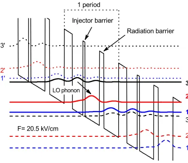
Radiation barrier
2
1
3
1"
2" 3"
1'
2'
1 period
Injector barrier
LO phonon
3'
[image:3.612.207.401.92.260.2]F= 20.5 kV/cm
Fig. 1. Calculated conduction band diagram and squared moduli of the electronic wave functions of a three-level design (D2) in GaAs/Al0.15Ga0.85As at an electric field of
20.5 kV/cm. Subbands 2 and 1 are the laser levels, and the carriers are injected from subband 3 to 2 by LO-phonon scattering. The layer sequence of an active module and the design parameters are listed in Table 1.
radiative transition [11, 15, 16]. Alternatively, an indirect injection scheme [17–22] can be used, in which LO-phonon scattering replaces resonant tunneling for carrier injection; QCL devices based on this indirect injection scheme have operated up to 163 K at 1.8 THz [19]. A simple ’extraction-controlled’ design has also been proposed [23], in which only one phonon scattering process is employed to realize both carrier extraction and injection simultaneously; this contrasts with the two LO-phonon scattering processes used for separate carrier extraction and injection in previous indirect injection schemes. Here, we present a new extraction-controlled design in which a diagonal LO-phonon extraction and injection stage is used to increase the carrier injection efficiency. Our design has only three subbands within each module, and its simplicity makes it an ideal platform to investigate the scattering injection process for high temperature operation of THz QCLs.
2. Active region design
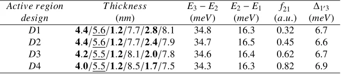
The conduction band profile and the squared moduli of the electronic wavefunctions of three periods of our GaAs/Al0.15Ga0.85As structure at the design bias are shown in Fig. 1. The ground
Table 1. Overview of the layer sequences and key parameters of the four designs. The layer thicknesses of one active module are given with the Al0.15Ga0.85As barriers in bold
and GaAs wells in plain text. The underlined wells are doped with Si at the level of 2.66×1016cm−3, 2.61×1016cm−3, 2.62×1016cm−3and 2.58×1016cm−3for D1−D4 respectively, yielding average bulk level of 5.0×1015cm−3per period.E3−E2is the energy
separation between subbands 3 and 2,E2−E1is the energy separation between subbands 2
and 1, f21is the scaled oscillator strength, and∆103is the anticrossing gap energy of the
subbands 10and 3. The principal difference between the four designs is the optical transition diagonality, which is characterized byf21.
Active r egion T hickness E3−E2 E2−E1 f21 ∆103
design (nm) (meV) (meV) (a.u.) (meV)
D1 4.4/5.6/1.2/7.7/2.8/8.1 34.8 16.3 0.32 6.7
D2 4.4/5.6/1.2/7.7/2.4/7.9 34.7 16.5 0.45 6.6
D3 4.2/5.5/1.2/8.1/2.0/7.8 34.6 16.4 0.62 6.7
D4 4.0/5.5/1.2/8.5/1.7/7.5 34.3 16.3 0.82 6.9
by the thickness of the radiation barrier, which separates the laser levels 2 and 1 into different quantum wells. As summarised in Table 1, four structures have been investigated with different degrees of optical transition diagonality.
3. Experiment results
The samples were grown on semi-insulating GaAs substrates by molecular beam epitaxy. A 300-nm-thick Al0.55Ga0.45As layer was first grown as an etch stop layer for use in the metal-metal
waveguide fabrication. Each QCL structure consisted of a 10-µm-thick periodic stack (consisting of 336, 343, 348, and 353 periods for D1−D4, respectively) of the three-well active modules,
embedded between two n+-GaAs layers. The lower GaAs layer was 100 nm thick and the upper
GaAs layer was 50 nm thick. Both layers were Si doped at a level of n = 5.0×1018cm−3. Following
growth, the QCL wafers were thermo-compression bonded to n+-GaAs acceptor wafers, and
devices were fabricated using a gold-gold waveguide configuration [24]. After removal of the growth substrate, a non-alloyed Ti/Au (10/150 nm) layer was deposited as the top waveguide layer and the laser ridges were etched in a H2SO4: H2O2: H2O (1:8:1) solution. After substrate
thinning to a thickness of 180µm, and back-side metallization, laser bars were cleaved and
indium-soldered to copper submounts. For the light power-current-voltage (L-I-V) and spectral
characterization, the devices were operated in pulsed mode with 2-µs-long pulses at a repetition rate of 10 kHz and the laser emission was detected using a cooled Ge:Ga photoconductive detector. In order to match the detector response time, the pulse train was gated with a slow 167 Hz modulation with 50% duty cycle. The output power was calibrated separately with an absolute THz power meter (Thomas-Keating Instruments) using a gate frequency of 30 Hz.
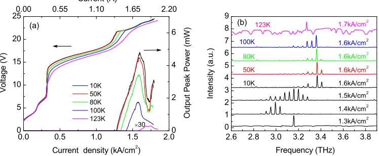
Figure 2(a) shows theL-I-Vcurves measured for design D2, for which f21= 0.45. The device
lased up to 123 K in pulsed mode, which is the maximum operating temperature of the four designs. At a temperature of 10 K, the threshold current density (Jth) was 1.29 kA/cm2, the
peak output power was 4.8 mW at a current density of 1.60 kA/cm2, and the slope efficiency
was 14 mW/A. The peak power is comparable with other indirect injection designs [20-22], but the current is much higher, resulting in significant Joule heating within the device. A regression of the temperature evolution of the threshold current density to the empirical equation
Jth = J0 +J1ex p(T/T0) yields the valueT0= 27 K. The small T0 indicates large thermally
activated current, resulting in a large threshold current density of 1.58 kA/cm2at 123 K. The
emission spectra measured at a range of biases are shown in Fig. 2(b). The emission frequency
0.0 0.5 1.0 1.5 2.0 0 5 10 15 20 25
0.00 0.55 1.10 1.65 2.20
2.6 2.8 3.0 3.2 3.4 3.6 3.8
0 1 2 3 4 5 6 7 8 9 Current (A) V o l t a g e ( V )
Current density (kA/cm
2 ) (a) 0 2 4 6 10K 50K 80K 100K 123K O u t p u t P e a k P o w e r ( m W ) 30 1.6kA/cm 2 1.6kA/cm 2 1.6kA/cm 2 50K 100K 80K I n t e n si t y ( a . u . ) (b) 1.7kA/cm 2 Frequency (THz) 1.6kA/cm 2 1.5kA/cm 2 1.4kA/cm 2 1.3kA/cm 2 123K 10K
Fig. 2. (a) Output power-current density-applied voltage (L-I-V) characteristics of design D2
at various temperatures. (b) Spectra at various current densities and temperatures. The device was 1000µm long and 110µm wide, processed into a gold-gold waveguide configuration, and operated in pulsed mode with 2-µs-long pulses at a repetition rate of 10 kHz.
With increasing bias, the spectra broadened and multi-mode lasing behavior was observed over the range 2.9 to 3.4 THz. When the temperature increased to 123 K, only the mode at 3.3 THz remained. TheI-Vcurve at 10 K exhibits three distinct step increases in the current density before
the threshold current is reached; the first increase to 0.20 kA/cm2, the second to 0.32 kA/cm2
and the third to 1.20 kA/cm2, with corresponding applied voltages roughly coincident with those
for the alignment of the subbands 1−100, 1−200and 2−300, respectively. These three increases of current are indicative of parasitic paths for the carrier transport, which might be related to the resonant coupling of the subbands described above. At elevated temperatures, the onset bias of the third current step decreases to 10.2 V, indicating thermal activation of the parasitic path.
The device performance is dependent on the diagonality of the optical transition. Four designs (D1−D4) with f21varying from 0.32 to 0.82 were investigated, and theI-Vcurves and emission
spectra measured at 10 K are compared in Fig. 3. As shown in Fig. 3(b), similar lasing frequencies at the design bias indicate good control over the material growth. The differences in theI-V
curves and the maximum operating temperatures can, therefore, be attributed principally to the difference in the oscillator strength f21. The key features of theI-Vcurves are the same in each
case, i.e., three distinct step increases in current are separated by regions of negative differential resistance (NDR) before the threshold is reached. The main difference between theI-Vcurves is
the marked increase in current for designs with large oscillator strengthf21, especially for the last
two current steps. With the increase off21(D1−D4), the current density rises to 0.22 kA/cm2
(D1) and 0.53 kA/cm2(D4) in the second step, and to 1.0 kA/cm2(D1) and 2.0 kA/cm2(D4) in
[image:5.612.120.494.99.253.2]0.0 0.5 1.0 1.5 2.0 2.5 0 5 10 15 20 25 30
2.4 2.6 2.8 3.0 3.2 3.4 3.6 3.8 4.0 4.2
0.0 1.0 2.0 3.0 4.0 10K D1 D2 D3 D4 V o l t a g e ( V )
Current density (kA/cm
2 ) (a) I n t e n si t y ( a . u . ) 10K D4 D3 D2 (b) Frequency (THz) 1.3 kA/cm 2 1.6 kA/cm 2 1.9 kA/cm 2 2.3 kA/cm 2 D1
0.2 0.4 0.6 0.8
80 100 120 140 D4 D3 D2 T m a x ( K )
Osci l l ator strength (a.u.) D1
Fig. 3. (a)I-Vcharacteristics of the four designs at 10 K. The regions of theI-Vcurves
shown in thicker lines indicate the lasing ranges. Inset: the maximum operating temperatures. (b) Spectra of the four designs at 10 K, measured at the conditions of maximum output power for each. All devices were processed into a gold-gold waveguide configuration, and operated with 2-µs-long voltage pulses at a repetition rate of 10 kHz.
4. Numerical results
To analyze the parasitic paths and the temperature performance degradation, an extended density matrix (DM) approach was used to simulate the carrier transport [27]. This approach is capable of modelling QCLs with an arbitrary number of subbands, and there is no need to manually designate an injector subband in advance. The subband wavefunctions for one period were calculated based on a tight-binding model, in which a period of the QCL structure is embedded between thick layers of the barrier material. These localized wavefunctions were also shifted along the growth direction to upstream and downstream periods, and three neighboring periods were selected in our DM approach. The assumption was made that carrier transport is determined only by interperiod resonant tunneling and intraperiod scattering. The coherence coupling of the subbands in the neighboring period was described by Rabi oscillations, with energy~Ω, across the barrier
separating the periods. This coherence coupling is closely related with the resonant tunneling time. The intraperiod transport was computed by Monte Carlo model [13] including phonon scattering, electron-electron scattering, ionized impurity scattering and interface roughness scattering (described by a Gaussian correlation function with an average root-mean-square step height of 0.12 nm and an in-plain correlation length of 10 nm).
For our design, the periods are separated by the thickest barrier, i.e., the extraction barrier, as shown in Fig. 1. Only three bound subbands in each period were considered and the effects of continuum states were neglected. Based on the sequential resonant tunneling model [28], the current is the sum of the tunneling current between neighboring periods,Ii j (i = 1−3, j = 100−300). The calculated and measured I-V curves are compared in Fig. 4. Stimulated emission was included self-consistently for the calculation of theI-Vcurve. A voltage drop of
2.5 V due to the Schottky barrier and a series contact resistance of 0.3Ωwere used to calibrate
the measuredI-V curve. The calculation shows a good agreement with experimental results,
[image:6.612.119.492.96.239.2]0 5 10 15 20 25 -0.5 0.0 0.5 1.0 1.5 2.0 J ( kA / cm 2 )
experi m ent
si m ul ati on
[image:7.612.208.405.94.242.2]Electric field (kV/cm) D2, 10K 0 20 40 60 80 100 G a i n ( cm -1 )
Fig. 4. Comparison of the calculated and measuredI-Vcurves (indicated by a dotted ellipse),
and the calculated gain as a function of the electric field, of design D2 at 10 K.
0 5 10 15 20 25
0.0 0.2 0.4 0.6 0.8 1.0 1.2 1.4 D2, 10K
Electric field (kV/cm)
J i '-i ( kA / cm 2 ) i '-1 i '-2 i '-3 (a)
0 5 10 15 20 25
0.0 0.2 0.4 0.6 0.8 1.0
Electric field (kV/cm) D2, 10K (b) 1-i " 2-i " 3-i " J i -i " ( kA / cm 2 )
Fig. 5. Calculated resonant tunneling current between neighboring periods of design D2 at 10 K. (a) Total injection current contribution from the upstream period to different subbands 1, 2, and 3. i0indicates subbands 10, 20and 30in the upstream period. (b) Total extraction current contribution from different subband levels to the downstream period. i00indicates subbands 100, 200and 300in the downstream period.
disagreement ofI-V curves at very high electric fields may be due to neglecting the current
through higher energy states and continuum states [25, 29].
[image:7.612.121.493.284.426.2]0 50 100 150 200 250 300 1
10
0 50 100 150 200 250 300
1 10
Temperature (K)
T
i
m
e
(
p
s)
3
3i"
31
32
(a) D2
D2 (b)
T
i
m
e
(
p
s)
Temperature (K)
1
2
21
[image:8.612.119.496.93.245.2]
2i"
Fig. 6. Temperature evolution of subband lifetime and the key carrier transport time for design D2. (a) The lifetime of subband 3 and the carrier transport time from level 3 to the lower subbands. (b) The lifetime of subbands 2 and 1, and the carrier transport time from level 2 to the lower subbands. i00indicates subbands 100, 200and 300in the downstream period.
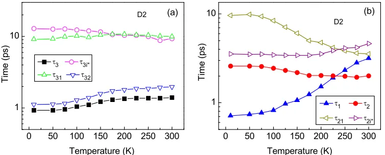
The first parasitic current path at a bias of 4.8 kV/cm is mainly from levels 10→2→1→200, where level 1 is aligned with level 200. When the electric field is higher than 12 kV/cm, levels 2 and 1 start to align with level 300. The carriers are then injected from levels 10and 20to level 3, relax to levels 2 and 1, and finally are extracted to level 300. The second parasitic current path is therefore from level 20→3→2→300and 10→3→1→300, where the first path is dominant since the scattering rate from level 3 to 2 is much larger than that from level 3 to 1 (shown in Fig. 6). The parasitic current along path 20→3→2→300contributes more than half of the total current at an electric field of 16.8 kV/cm, and 24% at the designed field of 20.5 kV/cm.
Figure 6 shows the temperature dependence of the lifetime of each subband and also the related carrier transport time for design D2 at the design bias. Electrons in level 3 can transport downstream to the next period by resonant tunneling, and to levels 2 and 1 by LO phonon scattering. As shown in Fig. 6(a), the resonant tunneling time to the next period (τ3i00) and the
scattering time to level 1 (τ31) are both∼10 ps, which is much longer than the scattering time to
level 2 (τ32), which is 1.1 ps. The strong LO phonon scattering between levels 3 and 2 dominates the carrier transport from level 3, and hence leads to the short lifetime of level 3,τ3= 0.93 ps at 10 K. Since the current from the upstream period is injected mainly to level 3 (see Fig. 5), the short scattering timeτ32gives a high carrier injection efficiency of 83%. For subband 2, as shown in Fig. 6(b), the resonant tunneling time (τ2i00) is much shorter than the scattering time
(τ21) at 10 K, which reduces the lifetime of the subband level toτ2= 2.6 ps. This short tunneling timeτ2i00is the reason for the large parasitic current from level 2 to 300. The lifetime of subband 1
0.3 0.4 0.5 0.6 0.7 0.8 0.9 0
4 8 12 16
31
13"
32
23"
T
i
m
e
(
p
s)
[image:9.612.207.402.91.256.2]Oscillator strength (a.u.) 10K
Fig. 7. Calculated carrier transport time of the key relaxation processes from subbands 3, 2 and 1 at the design biases for each versus the scaled oscillator strength.
for the carriers up to 237 K. The small increase ofτ32from 1.1 ps to 2.0 ps indicates the reduction of injection efficiency has less effect on the temperature performance.
To better understand the effects of the scaled oscillator strength f21, the calculated carrier
transport time at the design bias is shown in Fig. 7. In our design, the barrier separating the two active wells is thinned in order to increasef21. However, thinning this barrier also increases the
coupling of the levels 3−1 as well as the coupling of 2−300, which can be indicated by the
decrease ofτ31andτ2300. With the increase of f21, the stronger coupling of the levels 3−1 and
2−300results in more carriers transporting through these paths. Note thatτ2300is much smaller
thanτ31, which means the coupling of the levels 2-300dominates these parasitic paths for all four designs. This suggests that suppression of this strong parasitic coupling could result in better device performance, such as smaller current density and higher operating temperatures.
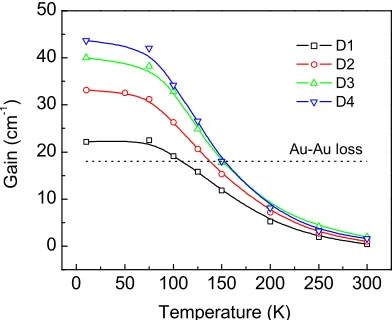
The optical gain (g ∝∆n21f21, where ∆n21 is the population inversion) has a complex
dependency on the diagonality of the optical transition. To estimate the device performance, the peak gain of the four designs was calculated and the results are shown in Fig. 8. At low temperature (10 K), LO phonon scattering between the laser levels is weak and an increase in
f21only results in a small decrease in∆n21. The gain therefore increases from 22.1 cm−1 to
43.6 cm−1as
f21varies from 0.32 to 0.82. At elevated temperatures, however, thermally activated
LO-phonon scattering becomes stronger, leading to a loss of population inversion. In this case, the thermal degradation becomes more significant with increasing f21because of the enhanced
LO phonon scattering between laser levels, and the maximum gain will consequently be obtained at an optimum value of f21. The estimated maximum operating temperatures (Tmax) for designs
D1 to D4 are 108 K, 137 K, 151 K and 153 K, respectively. The measured Tmaxare 103 K, 123 K,
113 K and 80 K, respectively, as shown in the inset of Fig. 3(a). The agreement for designs D1 and D2 is better than that for D3 and D4, and the difference between the calculated and measured Tmaxbecomes larger with increasing f21. A number of factors, which are not included in our
model, may contribute to this discrepancy, and will be discussed next.
5. Discussion
In order to better understand the device performance, several factors arising from our model need to be considered: (1) Continuum states and higher energy states; (2) Interface roughness; and (3) Joule heating. Firstly, our devices are designed to operate at high voltages, and theI-V curves at
0 50 100 150 200 250 300 0
10 20 30 40 50
D1
D2
D3
D4
Temperature (K)
G
a
i
n
(
cm
-1
)
[image:10.612.208.404.94.254.2]Au-Au l oss
Fig. 8. Calculated peak gain of the four designs as a function of the lattice temperature. The dotted line is the estimated loss of QCLs with gold-gold waveguide configurations.
there is a discrepancy between calculated and measuredI-Vcurves in the high voltage range. This
indicates that continuum states or higher energy states may assist carrier transport from bound states. Recently, thermally activated leakage into the continuum was found to be an important limiting factor for the temperature performance [25, 26]. This mechanism may contribute to the rapid rapid degradation of the performance of our designs with increasing temperature. As such, including this mechanism in the simulations may help to reduce the discrepancy between the measured and calculated maximum lasing temperatures, and also explain the sensitivity of the maximum lasing temperature to the oscillator strength [31]. Secondly, interface roughness scattering is particularly important in our design since our structures have thin quantum wells, leading to an increase in the number of interfaces. The distribution of interface roughness was found relevant for THz QCLs [32], and therefore an improved description of interface roughness in our model may help to better estimate the device performance. Thirdly, our devices operate with high currents, which may lead to much higher active region temperatures and electron temperatures through Joule heating. This is another possible reason for reduced performance, especially for the designs D3 and D4.
For further improvement of our structures, the parasitic current needs to be suppressed in the initial stages of alignment. In this respect, a thicker extraction barrier or an additional extractor well could be beneficial to weakening the coupling between the upper laser level and extractor level. Application of higher barriers is another option, which could also help to reduce the carrier leakage into the continuum.
6. Conclusion
Funding
The Engineering and Physical Sciences Research Council (EPSRC) (EP/J017671/1 and EP/J002356/1); European Research Council (ERC) (247375); European Space Agency; Centre for EO Instruments and Space Technology (CEOI-ST); Royal Society and Wolfson Foundation (WM110032, WM150029); ANR; European Research Council (ERC) (306661).
Acknowledgments