An Improved DCM-based Tunable True Random
Number Generator for Xilinx FPGA
Anju P. Johnson
Member, IEEE
, Rajat Subhra Chakraborty
Senior Member, IEEE
and
Debdeep Mukhopadyay
Member, IEEE
Abstract—True Random Number Generators (TRNGs) play a
very important role in modern cryptographic systems. Field
Programmable Gate Arrays (FPGAs) form an ideal platform for hardware implementations of many of these security algorithms. In this paper we present a highly efficient and tunable TRNG
based on the principle ofBeat Frequency Detection(BFD),
specifi-cally forXilinxFPGA based applications. The main advantages of
the proposed TRNG are its on-the-fly tunability throughDynamic
Partial Reconfiguration (DPR) to improve randomness qualities. We describe the mathematical model of the TRNG operations,
and experimental results for the circuit implemented on aXilinx
Virtex-VFPGA. The proposed TRNG has low hardware footprint and in-built bias elimination capabilities. The random bitstreams generated from it passes all tests in the NIST statistical testsuite.
Keywords—Digital Clock Manager, Dynamic Partial Reconfigu-ration, Field Programmable Gate Arrays, True Random Number Generator.
I. INTRODUCTION
True Random Number Generators (TRNGs) have become indispensable component in many cryptographic systems, in-cluding PIN/password generation, authentication protocols, key generation, random padding and nonce generation. TRNG circuits utilize a non-deterministic random process, usually in the form of electrical noise, as a basic source of randomness. Along with the noise source, a noise harvesting mechanism to extract the noise, and a post-processing stage to provide a uniform statistical distribution are other important components of the TRNG. Our focus is to design an improved FPGA based TRNGs, using purely digital components. Using digital building blocks for TRNGs has the advantage that the designs are relatively simple and well-suited to the FPGA design flow, as they can suitably leverage the CAD software tools available for FPGA design. However, digital circuits exhibit comparatively limited number of sources of random noise, e.g. metastability of circuit elements, frequency of free running oscillators and jitters (random phase shifts) in clock signals. As would be evident, our proposed TRNG circuit utilizes the frequency difference of two oscillators and oscillator jitter as sources of randomness.
Reconfigurable devices have become an integral part of many embedded digital systems, and predicted to become the platform of choice for general computing in near future. From
The authors are with the Secured Embedded Architecture Labora-tory (SEAL), Dept. of Computer Science and Engineering, Indian Insti-tute of Technology Kharagpur, Kharagpur, West Bengal, INDIA – 721302. Email:{anjupj,rschakraborty,debdeep}@cse.iitkgp.ernet.in.
being mainly prototyping devices, reconfigurable systems in-cluding FPGAs are being widely employed in cryptographic applications, as they can provide acceptable to high processing rate at much lower cost and faster design cycle time. Hence, many embedded systems in the domain of security require a high quality TRNG implementable on FPGA as a component. We present a TRNG for Xilinx FPGA based applications, which has a tunable jitter control capability based on DPR capabilities available on Xilinx FPGAs. The major contribution of this paper is the development of an architecture which allows on–the–fly tunabilty of statistical qualities of a TRNG by utilizing DPR capabilities of modern FPGAs for varying the DCM modeling parameters. To the best of our knowledge this is the first reported work which incorporates tunability in a TRNG. This approach is only applicable for Xilinx FPGAs which provide programmable clock generation mechanism, and capability of DPR.
DPR is a relatively new enhancement in FPGA technology, whereby modifications to predefined portions of the FPGA logic fabric is possible on–the–fly, without affecting the normal functionality of the FPGA. Xilinx Clock Management Tiles
(CMTs) contain Dynamic Reconfiguration Port (DRP) which allow DPR to be performed through much simpler means [1]. Using DPR, the clock frequencies generated can be changed on–the–fly by adjusting the corresponding DCM parameters. DPR via DRP is an added advantage in FPGAs as it allows the user to tune the clock frequency as per the need. Design techniques exist to prevent any malicious manipulations via DPR which in other ways may detrimentally affect the security of the system [2].
The goal of this paper is the design, analysis and implemen-tation of an easy-to-design, improved, low-overhead, tunable TRNG for the FPGA platform. The following are our major contributions:
1) We investigate the limitations of the BFD–TRNG [3] when implemented on a FPGA design platform. To solve the shortcomings, we propose an improved BFD–TRNG architecture suitable for FPGA based applications. To the best of our knowledge this is the first reported work which incorporates tunability in a fully digital TRNG.
2) We analyze the modified proposed architecture mathemat-ically and experimentally.
The rest of the paper is organized as follows: Section II discusses the preliminaries, followed by the proposed TRNG design in Section III. The mathematical model of the proposed design is discussed in Section IV. Section V describes the implementation and experimental results. We conclude in Section VI.
II. BACKGROUND ANDMOTIVATION
This section briefly describes the basic BFD–TRNG model and the DPR methodology utilizing DRP ports available in
XilinxCMTs.
A. Single Phase BFD-TRNG Model
The BFD-TRNG circuit [3] is a fully-digital TRNG, which relies on jitter extraction by the Beat Frequency Detection
[image:2.612.353.536.52.156.2](BFD) mechanism, originally implemented as a 65-nm CMOS ASIC. The structure and working of the (single phase) BFD-TRNG can be summarised as follows, in conjunction with Fig. 1:
1) The circuit consists of two quasi-identical ring oscillators (let us term them asROSCAandROSCB), with similar
construction and placement. Due to inherent physical randomness originating from process variation effects associated with deep sub-micron CMOS manufacturing, one of the oscillators (say, ROSCA) oscillates slightly
faster than the other oscillator (ROSCB). In addition,
the authors [3] proposed to employ trimming capacitors to further tune the oscillator output frequencies.
2) The output of one of the ROs is used to sample the output of the other, using a D flip-flop (DFF). Without loss of generality, assume the output of ROSCA is fed
to the D-input of the DFF, while the output ofROSCB
is connected to the clock input of the DFF.
3) At certain time intervals (determined by the frequency difference of the two ROCs), the faster oscillator signal passes, catches up, and overtakes the slower signal in phase. Due to random jitter, these capturing events happen at random intervals, called “Beat Frequency Intervals”. As a result, the DFF outputs a logic-1 at different random instances.
4) A counter controlled by the DFF increments during the beat frequency intervals, and gets reset due to the logic-1 output of the DFF. Due to the random jitter, the free-running counter output ramps up to different peak values in each of the count-up intervals before getting reset. 5) The output of the counter is sampled by a sampling clock
before it reaches its maximum value.
6) The sampled response is then serialized to obtain the random bitstream.
B. Shortcoming of the BFD-TRNG
One shortcoming of the previous BFD-TRNG circuit is that its statistical randomness is dependent on the design quality of the ring oscillators. Any design bias in the ring oscillators might adversely affect the statistical randomness of the bit-stream generated by the TRNG. Designs with same number of
Fig. 1: Architecture of single phase BFD–TRNG [3].
inverters but different placements resulted in varying counter maximas. Additionally the same ring-oscillator based BFD-TRNG implemented on different FPGAs of the same family shows distinct counter maxima. Unfortunately, since the ring oscillators are free-running, it is difficult to control them to eliminate any design bias. The problem is exacerbated in FPGAs where it is often difficult to control design bias because of the lack of fine-grained designer control on routing in the FPGA design fabric. A relatively simple way of tuning clock generator hardware primitives on Xilinx FPGAs, particularly
the Phase Locked Loop(P LL) or theDigital Clock Manager
(DCM) as used in this work, is by enabling dynamic reconfig-uration via the Dynamic Reconfiguration Ports(DRPs). Once enabled, the clock generators can be tuned to generate clock signals of different frequencies by modifying values at the DRPs [1] on–the–fly, without needing to bring the device off– line.
We next describe the proposed tunable BFD-TRNG suitable for FPGA platforms.
III. TUNABLEBFD–TRNGFORFPGABASED
APPLICATIONS A. Design Overview
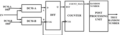
Fig. 2 shows the overall architecture of the proposed TRNG. In place of two ring oscillators, two DCM modules generate the oscillation waveforms. The DCM primitives are parameterized to generate slightly different frequencies, by adjusting two design parametersM (Multiplication Factor) andD(Division
Factor). In the proposed design, the source of randomness is
Fig. 2: Overall architecture of proposed Digital Clock Manager based tunable BFD–TRNG.
Fig. 3: Architecture of tuning circuity.
Additionally, we have a simple post-processing unit using a
Von Neumann Corrector (VNC) [5] to eliminate any biasing
in the generated random bits. VNC is a well-known low-overhead scheme to eliminate bias from a random bitstream. In this scheme, any input bit “00” or “11” pattern is eliminated; otherwise, if the input bit pattern is “01” or “10”, only the first bit is retained. The last three LSBs of the generated random number is passed through the VNC. The VNC improves the statistical qualities at the cost of slight decrease in throughput.
B. Tuning Circuitry
The architecture of the tuning circuitry is shown in Fig. 3. The target clock frequency is determined by the set of pa-rameter values actually selected. The random values reached by the counter, as well as the jitter are related to the chosen parameters M and D (details are discussed in Section IV). This makes it possible to tune the proposed TRNG using the predetermined stored M and D values. As unrestricted DPR has been shown to be a potential threat to the circuit [6], the safe operational value combinations of the D and M
parameters for each DCM are predetermined during the design time, and stored on an on-chipBlock RAM (BRAM) memory block in the FPGA.
There are actually two different options for the clock gen-erators – one can use the Phase Locked Loop (PLL) hard macros available on Xilinx FPGAs, or the DCMs. We next describe analytical and experimental results which compelled us to choose DCM in favor of the PLL modules for clock waveform generation.
IV. MATHEMATICALMODEL OFPROPOSEDTRNG
A. Circuit Behavior with PLL as Clock Generator
We first consider the operational principle for the PLL, and its feasibility as a component of the proposed TRNG. The
XilinxPLL synthesizes a clock signal whose frequency is given
by:
FCLKF X =FCLKIN·
M
D (1)
whereFCLKIN is the frequency of input clock signal, andM
and D are the multiplication and division factors previously mentioned. Values of M andD can be varied to generate the required clock frequency. The two PLLs can be parametrized with the necessary set of (M, D) values to generate two slightly different clock frequencies. Without loss of generality, assume P LLA is set up to be slightly faster thanP LLB, i.e.
the time periods are related byTA< TB. On reaching the beat
frequency interval (say,nclock cycles), by definition, P LLA
completes one cycle more than the slower one. The following equation depicts this simple model:
TA TB
= N
N+ 1 (2)
N = 2.n, wheren is the estimated maximum counter value. For the first n clock cycles, the counter does not increment, and then increments by one for each of the next n clock cycles. Hence, the maximum counter values reached is n. Then, Eqn. (2) leads to:
n=
T
B
2(TB−TA)
(3)
Using design configuration parameters (M and D) one of the oscillators is made to run faster than the other. This is done in order to limit the range of counter values produced. If both the oscillators were configured to run at the same frequency we may get random numbers, but the maximum counter value produced will be very high (theoretically infinite) as per Eqn. (3). In other words, the latency of the circuit will be very high, since the counter sets and resets only after reaching a very large count value. When the Xilinx PLLs are used as clock generators, the predicted and observed counter values for all combinations of (M, D)values remain the same. This confirms that the Xilinx PLL instances demonstrate close-to-ideal behavior and are quasi-identical, and have negligible jitter between the waveforms generated by them. Since the BFD-TRNG is critically dependent on the presence of jitter between the two generated clock waveforms, PLLs seem unsuitable as components of the proposed TRNG. Hence, next we examine the DCM as clock generators.
B. Circuit Behavior with DCM as Clock Generator
Without loss of generality, the clock signals produced by one of the DCM (say, DCMA) is slightly faster than the
other (DCMB), implying TA < TB. This is ensured by
assigning the design parametersM andDas in Eqn. (7). More details are discussed in Section IV-C. Timing diagrams of the
DCM clock outputs and the resultant DFF response is shown in Fig. 4. Let N be the number of clock cycles of the slower clock signal in which the faster clock signal completes exactly one cycle more. Then,
tA[N+ 1] = (N+ 1)TA+A (4)
and
tB[N] =N TB+B (5)
whereAandB are the uncertainties due to jitter inDCMA
[image:3.612.68.282.156.215.2]Fig. 4: Timing diagram of DCM output waveforms and the corresponding and DFF response.
TABLE I: Hardware Footprint of the Proposed TRNG‡ and the Ring Oscillator based TRNG
Design Module Name Slice SliceReg LUTs BUFG DCM ADV PLL ADV Oscillators 4 0 4 4 2 0
DCM-based TRNG DFF 1 1 0 0 0 0
Counter 9 25 15 30 0 0
Total 14 26 19 34 2 0
Oscillators 23 0 90 0 0 0
Ring Oscillator DFF 1 1 0 0 0 0
-based TRNG Counter 9 25 15 30 0 0
Sampler 0 0 0 1 0 1
Total 33 26 15 31 0 1 ‡
The hardware footprint excludes theMicroBlazesoft processor necessary for overall control and data acquisition from the TRNG, and 46 bytes of memory required in the BRAM module to store the 23 feasible(M, D)calculations.
TABLE II: On-Chip Power Dissipation? of the Proposed TRNG and the Ring Oscillator based TRNG‡
On-Chip Clock Logic Signal BRAM PLL DCM IO Leakage Total DCM 0.098 0.001 0.002 0.003 0.134 0.136 0.034 1.062 1.470
-based TRNG
Ring Oscillator 0.053 0.000 0.002 0.000 0.268 0.000 0.000 1.061 1.384
-based TRNG
?
Power dissipation in watt.
‡
Sampling clock frequency is103.1992kHz.
DCMA andDCMB are different, this is because the DCMs
are designed with distinct modeling parametersM andD. The corresponding jitter for each of the DCMs used in the proposed design is presented in Table III. For example, consider the configuration presented in Sl.No. 1. In this case, DCMA is
configured with M=15 andD=31 andDCMB is configured
with M=14 andD=29. This results in peak-to-peak jitter of
0.600 ns and 0.568 ns for DCMA andDCMB respectively.
Of course, we also have: tA[N + 1] = tB[N]. Assuming
there is no metastability for the DFF if signal transitions occur in the setup-hold timing window around its driving clock edge (the metastability issue can be avoided by cascaded DFF combination), the transition time (td) of the DFF, the time
interval after which it sets (i.e. the counter driven by the DFF resets), is estimated by:
td=
tA[N+ 1] +tB[N]
2 =
(N+ 1)TA+N TB+A+B
2
(6) From Eqn. (6), the transition time of DFF is a random process. The output of the DFF, i.e. the time interval (td) after which
the counter resets, is thus a random function. As a result, the count value obtained when the counter resets is also a random quantity. The counter resets automatically when the DFF sets, and the operation continues. The DFF resets approximately n
cycles after it sets, and the counter starts counting again.
C. Tuning Parameter Value Ranges
Eqns.(1)–(2) also holds true forDCM based beat frequency detection also. Hence, we have the following relationships:
D1·M2
D2·M1
= N
N+ 1
2≤Mi≤33,
1≤Di≤32,
400≤N ≤1000, Mi, Di, N∈Z.
(7)
where, M andD values are as per theXilinx DCM specifica-tion [1]. The count value to be sampled was set to be between
200 and 500, hence the values of N are as per Eqn. (7). Higher value of count is not desired, as it leads to higher power dissipation. As per Eqn. (7), there are 23 sets of(M, D)value combinations for the two DCMs, which satisfy the required count range. These values are stored in a BRAM, and for 23 distinct pairs we require5bit address line for selecting one of the combinations ofM andDvalues, and if the BRAM is con-figured to hold 16-bit words, we require 46 bytes of memory. The address increments to the required BRAM location where the corresponding values of theDCMB is stored on demand,
using a simple address generation module. In this way, using a restricted DPR methodology, the designer has control over the DCM configuration to choose the best combination generating random numbers with the best statistical quality. In order to avoid malicious modifications via DPR, we have enabled DPR restrictively by storing the allowable modelling parameters. In order to implement this secure tunable design slightly higher hardware overhead and power dissipation is required. The DCM-DRP controller initiates DPR in DCMA and DCMB
using standard Xilinxdesign methodology [1].
V. EXPERIMENTALRESULTS
The proposed circuit was designed using Verilog HDL, and implemented using Xilinx ISE (v 14.5) CAD software platform targeting the Xilinx Virtex-V FPGA platform. The DCM-DRP controller was implemented using the MicroBlaze
soft processor directly core directly instantiable in a Xilinx
FPGA. Table-I shows the hardware resource requirements results of the proposed TRNG, excluding the soft processor and the BRAM memory. This table also compares the hardware resource incurred in the design of ring oscillator-based BFD-TRNG which configured with target (nominal) time period of
38.00 ns (89 inverters). The clock signals produced by the DCMs are sets of values of the design parameters M and
[image:4.612.54.297.223.299.2]TABLE III: Experimental and Estimated Results of Counter Value Distribution
Sl.No. DCM-1 DCM-2 Counter M D Output Freq. Period Jitter Period Jitter M D Output Freq. Period Jitter Period Jitter Estimated Experimental
(MHz) (unit interval) (ns) (pk-to-pk) (ns) (MHz) (unit interval) (ns) (pk-to-pk) (ns) Max. Count Mean Relative Std. Dev. (%)
1 15 31 48.3871 0.029 0.600 14 29 48.2759 0.027 0.568 217 215 0.7683 2 21 22 95.4545 0.043 0.453 20 21 95.2381 0.042 0.436 220 218 1.1735 3 17 21 80.9534 0.035 0.436 21 26 80.7692 0.042 0.518 220 217 3.0310 4 20 27 74.0741 0.040 0.535 17 23 73.9130 0.035 0.469 229 224 6.3010 5 15 29 51.7241 0.029 0.568 16 31 51.6129 0.031 0.600 232 225 5.4424 6 17 25 68.0000 0.034 0.502 19 28 67.8571 0.037 0.551 237 236 1.2370 7 22 23 95.6522 0.045 0.469 21 22 95.9545 0.043 0.453 241 239 3.3484 8 19 29 65.5172 0.037 0.568 17 26 65.3846 0.034 0.518 246 241 5.0744 9 19 32 59.3750 0.037 0.617 16 27 59.2593 0.032 0.535 256 254 1.0534 10 22 31 70.9677 0.043 0.600 17 24 70.8333 0.034 0.486 268 263 0.8939 11 23 24 95.8333 0.047 0.486 22 23 95.6522 0.045 0.469 269 257 4.6929 12 19 25 76.0000 0.038 0.502 22 29 75.8621 0.043 0.568 275 271 1.0690 13 24 25 96.0000 0.048 0.502 23 24 95.8333 0.047 0.486 287 283 1.9877 14 21 32 65.6250 0.040 0.617 19 29 65.5172 0.037 0.568 304 302 0.9336 15 23 31 74.1936 0.045 0.060 20 27 74.0741 0.040 0.535 310 308 1.2826 16 25 26 96.1538 0.050 0.518 24 25 96.0000 0.048 0.502 312 300 5.3238 17 21 26 80.7692 0.042 0.518 25 31 80.6452 0.048 0.600 325 317 5.0382 18 26 27 96.2963 0.052 0.535 25 26 96.1538 0.050 0.518 337 333 1.8000 19 27 28 96.4286 0.053 0.551 26 27 96.2963 0.052 0.535 364 387 1.5485 20 28 29 96.5517 0.055 0.568 27 28 96.4286 0.053 0.551 391 388 1.7102 21 29 30 96.6667 0.056 0.584 28 29 96.5517 .055 0.568 420 398 14.3593 22 30 31 96.7742 0.058 0.600 29 30 96.6667 0.056 0.584 449 446 3.8755 23 31 32 96.8750 0.060 0.6170 30 31 96.5542 0.058 0.600 480 468 3.6902
was observed between the two ring oscillators. Additionally, hardware resource and power consumption varies with differ-ent clock frequency of the ring oscillator. Also, this design is vulnerable to Hardware Trojan Horse (HTH) insertions imposed on sampling clocks [7]. Table-II shows the power analysis report of the proposed TRNG and the Ring Oscillator based BFD-TRNG, the proposed design has about 6% power overhead compared to BFD-TRNG. Assuming an average TRNG count of 271 (corresponding to memory location 12), counter operating at 75.8621 MHz (corresponding toDCMB),
50% bits rejected by the Von Neumann Corrector, and 3 bits per random number retained, the Power-delay Product(PDP) of the proposed TRNG is 3.50 mJ per kilobit.
The tunable sets of DCM parameters, and the resultant theoretical and experimental random numbers are shown in Table-III. To understand the results, consider the configuration presented in Sl.No. (1) in the table. In this case, DCMA
is configured with M = 15 and D = 31, and DCMB is
configured withM = 14andD= 29. This results in peak-to-peak jitter of 0.600 ns and0.568 ns forDCMA andDCMB
respectively. The resulting clock frequencies synthesized are
48.3871MHz and 48.2759 MHz respectively. The estimated counter values as per Eqn. (3) is 217, and the corresponding mean of the counter value distribution obtained experimentally is 215. Hence, there is a relative deviation of0.7683.
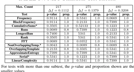
The statistical performance of the design is shown in Table-IV. This table presents the p-values and proportions corre-sponding for the individual NIST tests on the generated ran-dom numbers with mean217,275and480respectively (corre-sponding to results for three separate cases: (Sl. No. 1,12, and 23 considered in Table III). From the results, it is evident that the proposed TRNG exhibits excellent randomness properties at low hardware footprint and low power dissipation.
VI. CONCLUSION
[image:5.612.328.558.268.393.2]We have presented an improved fully digital tunable TRNG for FPGA based applications, based on the principle of Beat Frequency Detection and clock jitter, and with in-built error-correction capabilities. The TRNG utilizes this tunability fea-ture for determining the degree of randomness, thus providing
TABLE IV: NIST Statistical Test Results‡
Max. Count 217 275 480
∆f= 0.1112 ∆f= 0.1379 ∆f= 0.3208
Test p-value prop. p-value prop. p-value prop.
Frequency 0.9114 1.0 0.5341 1.0 0.0669 1.0
BlockFrequency 0.9114 1.0 0.2133 1.0 0.7399 1.0
CumulativeSums* 0.3505 1.0 0.52133 1.0 0.1223 1.0
Runs 0.0089 0.8 0.7399 1.0 0.1223 0.8
LongestRun 0.7400 1.0 5341 1.0 0.2133 1.0
Rank 0.3505 1.0 5341 1.0 0.5341 1.0
FFT 0.0089 1.0 0.0352 1.0 0.5341 1.0
NonOverlappingTemp.* 0.0043 1.0 0.0089 0.8 0.0089 0.8
OverlappingTemplate 0.2133 0.8 0.3505 1.0 0.5341 1.0
ApproximateEntropy 0.7399 1.0 0.7399 1.0 0.5341 0.9
Serial* 0.5341 1.0 0.1223 1.0 0.7399 1.0
LinearComplexity 0.9114 1.0 0.5341 1.0 0.7399 1.0
‡
For tests with more than one subtest, thep-value and proportion shown are the smaller values.
a high degree of flexibility for various applications. The proposed design successfully passes all NIST statistical tests.
REFERENCES
[1] Xilinx, Inc., “Virtex-5 FPGA Configuration User Guide UG 191 (v3.11)”, [Online]. Available: www.xilinx.com/support/documentation/ user guides/ug191.pdf, Accessed: May 2016.
[2] A. P. Johnson, R. S. Chakraborty and D. Mukhopadhyay, “A PUF-Enabled Secure Architecture for FPGA-Based IoT Applications,” inIEEE Transactions on Multi-Scale Computing Systems, vol. 1, no. 2, pp. 110-122, April-June 1 2015.
[3] Q. Tang, B. Kim, Y. Lao, K. K. Parhi and C. H. Kim, “True Random Number Generator circuits based on single- and multi-phase beat fre-quency detection,” Proceedings of the IEEE 2014 Custom Integrated Circuits Conference, pp. 1-4, September 2014.
[4] A. Rukhin, J. Soto, J. Nechvatal, M. Smid and E. Barker, “A Statistical Test Suite for Random and Pseudorandom Number Generators for Cryptographic Applications”,DTIC Document, Tech. Rep., 2001. [5] J. Von Neumann, “Various Techniques used in Connection with Random
Digits.”,National Bureau of Standards Applied Mathematics Series, vol. 12, pp. 36-38, 1951.
[6] A. P. Johnson, S. Saha, R. S. Chakraborty, D. Mukhopadyay and Sezer G¨oren ,“Fault Attack on AES via Hardware Trojan Insertion by Dynamic Partial Reconfiguration of FPGA over Ethernet”,9th Workshop on Embedded Systems Security (WESS 2014), October 2014.
![Fig. 1: Architecture of single phase BFD–TRNG [3].](https://thumb-us.123doks.com/thumbv2/123dok_us/7852339.178495/2.612.353.536.52.156/fig-architecture-of-single-phase-bfd-trng.webp)