Theses Thesis/Dissertation Collections
12-2017
The Design of a Custom 32-Bit SIMD Enhanced
Digital Signal Processor
Shashank Simha
Follow this and additional works at:http://scholarworks.rit.edu/theses
This Master's Project is brought to you for free and open access by the Thesis/Dissertation Collections at RIT Scholar Works. It has been accepted for inclusion in Theses by an authorized administrator of RIT Scholar Works. For more information, please [email protected].
Recommended Citation
The Design of a Custom 32-bit SIMD Enhanced Digital Signal Processor
by
Shashank Simha
Graduate Paper
Submitted in partial fulfillment of the requirements for the degree of
Master of Science
in Electrical Engineering
Approved by:
Mr. Mark A. Indovina, Lecturer
Graduate Research Advisor, Department of Electrical and Microelectronic Engineering
Dr. Sohail A. Dianat, Professor
Department Head, Department of Electrical and Microelectronic Engineering
Department of Electrical and Microelectronic Engineering Kate Gleason College of Engineering
Rochester Institute of Technology Rochester, New York
Declaration
I hereby declare that except where specific reference is made to the work of others, the contents of this paper are original and have not been submitted in whole or in part for consideration for any other degree or qualification in this, or any other University. This paper is the result of my own work and includes nothing which is the outcome of work done in collaboration, except where specifically indicated in the text.
I would like to thank my advisor, professor, and mentor, Mark A. Indovina, for all of his guidance throughout the entirety of this project. The continuous feedback and motivation provided by him has been a major driving force to push myself beyond limits throughout my career at RIT, for which I am truly grateful. His passion for teaching, expertise in digital design, along with decades of industrial experience has established him as my role model in the field. His advice, methods of teaching, managing and cross-domain knowledge has been a huge inspiration for me to pursue a career in the VLSI and digital design.
I would like to thank Dr. Dorin Patru and Dr. Marcin Lukowiak for providing me valuable knowledge and feedback in topics of computer architecture and FPGA, which provided a firm foundation in my understanding of the topics.
I would like to thank my parents for their continuous support throughout my career at RIT, believing in me and my being biggest role models. They have always been my pillars of support and great motivators throughout my life, at and away from home.
I would also like to thank my roommates for being my brothers throughout the two years of graduate school.
Abstract
For a number of years, the hardware industry has seen a drastic rise in embedded appli-cations. Thanks to the Internet of Things (IoT) revolution, a majority of these embed-ded applications are shifting towards the usage of simple hardware capable of running on batteries, while being able to handle complex data and implement complex algorithms. Translating these requirements to digital design terms, the hardware is expected to have high power efficiency, be tiny and simple enough, while being capable of meeting real-time constraints and process mathematical algorithms. Looking at some of the modern DSPs, most of them have been targeting high performance and wider applications, usually resulting in higher power consumption and complex hardware.
Declaration ii
Acknowledgements iii
Abstract iv
Contents v
List of Figures vii
List of Tables viii
1 Introduction 1
1.1 DSP classifications . . . 2
1.2 History of DSPs . . . 3
1.3 Brief introduction to the DSP design and paper organization . . . 6
2 DSP architecture 8 2.1 Top level block diagram . . . 10
2.2 Internal blocks . . . 11
2.2.1 Address decode unit . . . 12
2.2.2 Execution unit . . . 13
2.2.3 ALU . . . 15
3 Instruction Set Architecture of the DSP 17 3.1 Instruction and data word expansion . . . 18
3.2 Addressing modes . . . 18
3.2.1 Direct addressing . . . 21
3.2.2 Indirect addressing . . . 22
3.3 Instruction opcodes and operation . . . 23
3.3.1 List of instructions and corresponding opcodes . . . 23
Contents vi
4 DSP Pipeline and Read/Write RAM buffer wrapper implementation 32
4.1 Pipeline implementation . . . 33
4.1.1 Pipeline stages . . . 33
4.1.2 Pipeline design for non-branching instructions . . . 35
4.1.3 Pipeline design for unconditonal branching instructions . . . 37
4.1.4 Pipeline design for conditional branching instructions . . . 40
4.2 Read/write RAM buffer wrapper . . . 43
4.2.1 RAM read/write problem description . . . 44
4.2.2 Design and implementation of read/write buffer wrapper . . . 45
5 Median filter design 47 5.1 Median filter overview . . . 48
5.2 Median filter design and implementation . . . 48
6 Results 52 6.1 Results . . . 52
7 Conclusions and future work 54 7.1 Conclusion . . . 54
7.2 Future work . . . 54
References 56
I Source Code I-1
I.1 RTL source code . . . I-1
I.1.1 DSP top level module . . . I-1
I.1.2 ALU . . . I-25
I.1.3 Input shifter . . . I-32
I.1.4 Output shifter . . . I-35
I.1.5 Compare select unit . . . I-38
I.1.6 Multiplier . . . I-39
I.1.7 Adder . . . I-40
I.2 Assembler designed in Perl . . . I-41
I.3 Assembly source code for testing and median filter . . . I-55
I.3.1 Assembly code used for basic level testing . . . I-55
1.1 Fixed and floating point illustration . . . 2
2.1 Top-level block diagram . . . 10
2.2 Address decode unit block diagram . . . 13
2.3 Execution unit block diagram . . . 14
2.4 ALU block diagram . . . 16
3.1 Instruction word expansion for various instructions . . . 19
3.2 Data word exapansion . . . 20
3.3 Direct addressing illustration . . . 22
3.4 Indirect addressing illustration . . . 23
4.1 Pipeline stages and implementation . . . 34
4.2 Pipeline example for memory read instructions . . . 36
4.3 Pipeline example for memory write instructions . . . 38
4.4 Pipeline example for unconditional branching . . . 40
4.5 Pipeline implementation example for conditional branch instruction, when condition is false . . . 42
4.6 Pipeline implementation example for conditional branch instruction, when condition is true . . . 43
4.7 Read/write RAM buffer wrapper state machine . . . 45
5.1 Median filter working illustration . . . 49
5.2 Median filter algorithm . . . 49
List of Tables
3.1 List of Instructions and their opcodes . . . 23
3.1 List of Instructions and their opcodes . . . 24
3.1 List of Instructions and their opcodes . . . 25
3.1 List of Instructions and their opcodes . . . 26
3.1 List of Instructions and their opcodes . . . 27
3.2 List of instructions and their operations . . . 28
3.2 List of instructions and their operations . . . 29
3.2 List of instructions and their operations . . . 30
3.2 List of instructions and their operations . . . 31
Introduction
1.1 DSP classifications 2
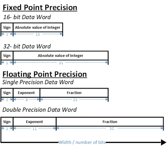
Figure 1.1: Fixed and floating point illustration
1.1
DSP classifications
DSPs are broadly classified into fixed and floating-point architectures. Fixed-point DSPs are designed to handle positive or negative integer data, while floating-point DSPs are designed to handle rational number data. The representation of data stored in each of these DSPs hence is different, which is the major reason behind the classification since it directly affects the amount of hardware required for each implementation. The fixed-point data is represented by the integer’s sign in the MSB (Most Significant Bit) followed by its value in the following bits. Floating-point data is represented by the rational number’s sign in the MSB, followed by its exponent, and later its mantissa. Fig. 1.1 illustrates fixed and floating point representations.[4]
[image:12.612.176.443.106.344.2]trades-off all these factors for better precision and faster computation of floating point data. Hence most of the times, either of the architectures is selected mainly based on the application. It is also worth noting that some DSPs are equally efficient in implementing either architectures like the SHARC DSP by Analog Devices.
Architecturally, the amount of hardware and design effort required to implement float-ing point precision is obviously much higher than fixed point precision. First, the data unit must be expanded from 16-bits to 32-bits at least along with the memory and registers. The ISA itself would have to be expanded significantly as almost all floating point DSPs usually support fixed point operations along with floating point ones [5].
From a compilation point of view, C language has an in-built type for floating-point to fully exploit the hardware capability of floating point DSPs. While the C compiler takes advantage of the floating point hardware, some rules and regulations are followed to ensure that the data fits within the 32-bit or 64-bit data word. Fixed point C compilation is implemented by mapping integers to fixed point data. The problem with fixed point though is that there is no ANSI standard for fixed point, hence it usually requires additional code for conversions and shifts. The efficiency of fixed point compilation takes another dip, since fixed point specific instructions are not built-in [6].
1.2
History of DSPs
1.2 History of DSPs 4
applications ranging from audio systems, speech processing, SONAR to medical imaging, RADAR, DSPs are used almost in every field today [7]. It is also interesting to note early applications of DSPs in personal computers like the Motorola 56000 used in the Atari Falcon, NeXT and SGI workstations.
DSPs have been produced by almost all major semiconductor companies including Intel, AMD, Texas Instruments, Motorola and Analog Devices at some point of time. Most of the early DSPs targeted audio processing, such as the Speak & Spell by Texas Instruments. Throughout the evolution of DSPs, they have grown more and more application specific over time, rather than the other way around [5].
Speak & Spell, an early toy used to teach kids to spell words, launched in 1976, was the earliest mass-produced DSP product in the market, powered by the Texas Instrument TMS5100 DSP [8]. Interestingly, in the late 70’s Intel unsuccessfully tried to enter the DSP market early with their 2920 analog processor, which failed mainly because of the absence of a true multiplier. The first attempts of DSP devices include the AT&T DSP1 and NEC µPD7720. It is worth noting that DSP1 introduced the historic MAC instruction to the world, this was one of the earliest steps of implementing instruction level parallelism in DSPs [9].
The first generation of DSPs started appearing in the market in the early 1980’s. Some key features of the DSPs of this generation were Harvard architecture and multiply-add-accumulate instructions. The TMS32010, from this generation of DSPs, by Texas In-struments was notably one of the most successful DSPs in history, as it pushed Texas Instruments to be the market leader in DSPs. Since it was based on Harvard architecture and with specialized ISA, it was the fastest DSP at the time [9].
DSP market with their popular fixed-point DSP56000 featuring 24-bit program and data words. The second generations of DSPs featured further optimization in memory architec-ture, with architectures capable of accessing multiple data memories in a single instruction. This generation also brought floating-point DSP architecture into market. Examples for this include the SHARC series of DSPs by Analog Devices, calling the architecture Super Harvard architecture. Interestingly, shrinking fabrication technology also had a huge im-pact on this generation of DSPs, as more and more hardware could be fit into the chip while still keeping it tiny in size [9].
Late 90’s DSPs incorporated more application-specific instructions, as they were mostly used as coprocessors along with the main CPU. Many DSPs however lost market when CPUs became SIMD capable. Parallel processing capabilities were subsequently introduced with Single Instruction Multiple Data (SIMD) and Very Long Instruction Word (VLIW) instructions in the later DSPs. VLIW architectures take advantage of spatial parallelism along with temporal parallelism, since they utilize several functional units to concurrently execute multiple operations, while pipelining these functional units [10]. Parallelism was further boosted with adding multiple cores and threads in later DSPs [9].
1.3 Brief introduction to the DSP design and paper organization 6
capabilities into the architecture. DSPs from LSI Logic Corp. take a different approach with their super-scalar architecture, while arguing that superscalar architecture is more compiler friendly compared to VLIW approach [9].
1.3
Brief introduction to the DSP design and paper
organization
The capabilities of DSPs have evidently evolved at a rapid pace over time, especially since the 90’s. With the introduction of concepts such as super Harvard architecure, VLIW and super-scalar architecture, the design complexity of DSPs has also risen at the same pace. Hence, the need for a simple embedded programmable processor with not only conventional instructions, but also DSP specific becomes desirable in some applications [12][13][14][15]. The paper [12] shows one such approach where, the TMS32010, a fairly simple monolithic DSP, is implemented on an FPGA platform.
major enhancements in our DSP design.
Chapter 2
DSP architecture
The DSP architecture is very different from that of a general-purpose CPU as discussed in the previous chapter. One of the biggest bottlenecks in executing DSP algorithms is transferring information to and from memory [5]. Things like Harvard architecture, direct memory access (DMA), multiply-accumulate unit (MAC) and barrel shifting are some features which distinguish DSPs from general purpose processors. Some DSPs have general purpose registers, like the SHARC ADSP-2106x, and others are accumulator based, such as the TMS32010 [5].
dependencies, and off course can not use the same resources. DSP architecture is usually designed by combining both techniques to accomplish the speed.
The DSP’s architecture being its most important feature, its significant difference of the from that of conventional microprocessors comes obvious. The basic capability of inte-grating a multiplier/ accumulator into its data-path has been proven to be revolutionary in computing multiple algorithms. Other factors such as preserving the precision of the prod-uct after multiplication, having shift capability while storing accumulator into the memory and handling overflow are crucial for DSP architecture, since most of its applications are usually complex arithmetic operations, requiring precise calculations [18].
2.1 Top level block diagram 10
2.1
Top level block diagram
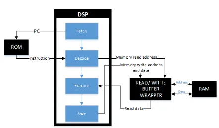
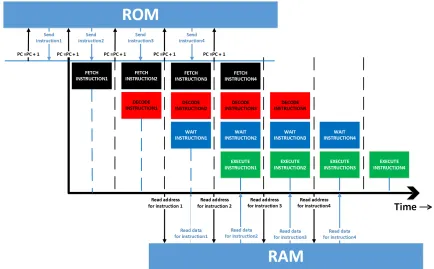
Figure 2.1: Top-level block diagram
The top-level block includes the DSP, ROM, RAM and read/write buffer wrapper. Fig.
2.1 attempts to visually describe the top-level view of the DSP system along with an abstracted high-level view of the interconnections between these components. It is to be noted that all the modules within the DSP are functional blocks, not pipeline stages. And, the necessity and usage of read-write RAM buffer is explained in chapter 4.
[image:20.612.83.525.126.385.2]result. Lastly, depending on the following instruction, this result is saved into the RAM via the read/write RAM buffer.
2.2
Internal blocks
As discussed in the previous section, the DSP needs to perform the following functions for every instruction in the same order:
1. Fetch the instruction from ROM,
2. Decode this instruction,
3. Fetch data from RAM if necessary,
4. Execution the instruction, and
5. Save the result back into the RAM if required.
While the pipeline takes care of distributing these functions across multiple clock cycles, it is necessary to carefully plan the hardware necessary to perform each function.
2.2 Internal blocks 12
2.2.1
Address decode unit
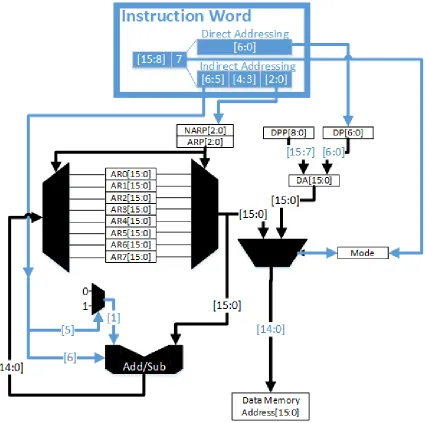
Fig.2.2 shows the block diagram of decode unit. The decode unit supports two addressing modes, namely direct and indirect addressing modes. As clearly shown in the figure, eight Auxiliary Registers (ARs) are used for indirect addressing. The AR pointer (ARP) is used to indicate which AR is to be used. Chapter 3 discusses addressing modes in detail.
Direct addressing does not require much logic to decode, as the instruction itself con-tains almost all required details to generate the data memory address. Here, the least significant or LSB 7-bits of the instruction is simply concatenated with the contents of the data page pointer (DPP) to generate the data memory address.
Figure 2.2: Address decode unit block diagram
2.2.2
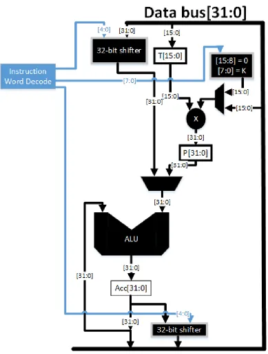
Execution unit
[image:23.612.100.525.103.526.2]2.2 Internal blocks 14
between these blocks, as directed by the instruction word decode logic.
[image:24.612.114.503.135.647.2]Two 32-bit barrel-shifters are used in the DSP. The input shifter is used to shift one of the ALU inputs, while the output shifter is used to shift the result of the ALU. The input data to the first shifter is read from the RAM. The second shifter is however used only while storing or writing back the accumulator contents into the RAM.
A 16x16 bit multiplier is used for multiplication operations. While one input to the multiplier always comes from the T-register, the other input can either be read from the RAM, or directly read from the instruction. The output however is always stored in the P-register.
The DSP is designed such that one of the ALU inputs is always the accumulator, while the other input is loaded either from the output of the first shifter or from the P-register. The result of the ALU is always fed back into the accumulator.
2.2.3
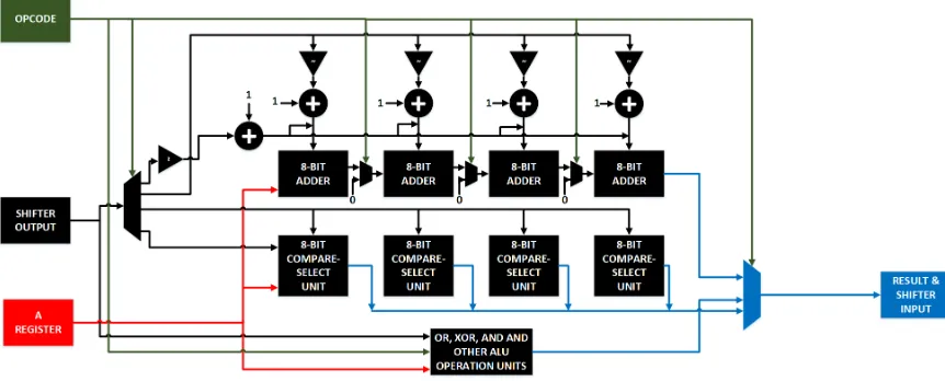
ALU
To accommodate SIMD instructions into the ISA, the ALU is optimized for add/subtract SIMD instructions. Fig. 2.4 shows the block diagram of the ALU. The main goal while de-signing the ALU was to add minimal hardware to TMS32010 design, while also supporting SIMD instructions.
2.2 Internal blocks 16
[image:26.612.89.520.301.475.2]Instruction Set Architecture of the
DSP
One of the biggest challenges while designing a DSP is to strike a fair balance between the hardware complexity for implementing a particular ISA (Instruction Set Architecture), and possible applications of almost every instruction. For the past few decades, major DSP manufacturers have been experimenting with different instructions and ISAs to maximize the applications of their DSPs across various fields. While having a complex ISA and hundreds of instructions looks like a clear winner, a significantly huge number of DSPs are used in embedded and real-time applications where power, size and cost are extremely important. Interestingly, with the advent of Internet of things (IoT), there has been an exponential increase in such applications. Here, ISA complexity needs to be traded off for flexibility and robustness.
3.1 Instruction and data word expansion 18
numerous general-purpose registers are used as ALU operands. And, it is quite obvious that most of the DSP operations would be ALU operations. [19]
The proposed DSP architecture is very similar to TMS32010 in its ISA. In the next few sections, the instruction and data words of the DSP, addressing modes and instruction opcodes along with operations are briefly described.
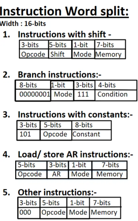
3.1
Instruction and data word expansion
To be able to fit in all the instructions and corresponding data required for each instruction within 16-bits of instruction word, five types of instruction words are planned. Fig. 3.1
shows the expansions of these instruction words. It is to be noted that the expansions indi-cated in the figure are only for direct addressing mode. In the case of indirect addressing, the last 7-bits are used differently. Bits 0, 1 and 2 are used to indicate the value of next AR pointer (NARP), while bits 5 and 6 are used to indicate post increment/decrement operation for the current AR.
Data words can be stored in four different formats, depending on the type of instruction used to handle them. Fig. 3.2 shows all variants of data word, where D0, D1, D2 and D3 are 8-bit signed/unsigned integers. While all instructions handled by the ALU are 32-bit data words, SIMD instructions use the 8-bit variants.
3.2
Addressing modes
3.2 Addressing modes 20
contains a much larger RAM, the data-page pointer here has been expanded to 8-bits from TMS32010’s single or double bit versions. [20].
Since multiplication is the only instruction which supports immediate addressing, the DSP does not really support immediate addressing when it comes to any other operations, including ALU operations. Therefore, immediate addressing is not claimed to be supported by the DSP.
3.2.1
Direct addressing
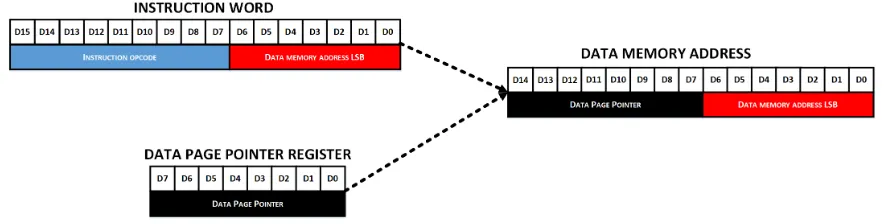
Though direct addressing seems fairly straight forward in implementation, it involves a two-step process. In the first step, the data-page pointer register needs to be loaded with the value of the most significant or MSB 8-bits of the address, using a separate load data-page pointer instruction. The second step is to specify the remaining 7-bits of the address in the least significant or LSB 7-bits of the instruction, while resetting the eighth bit of the instruction to indicate direct addressing mode.
3.2 Addressing modes 22
Figure 3.3: Direct addressing illustration
3.2.2
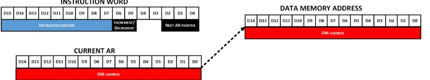
Indirect addressing
Indirect addressing is a multi-step process, since it accomplishes two things: selecting the next auxiliary register (AR) and incrementing/decrementing the current AR. The ARs hold address locations for the RAM data to be fetched, hence it is required to load them prior to using indirect addressing instructions.
The first step is to load one or more ARs with the value of the desired address location/s. Next, the AR pointer (ARP) needs to be set to the AR containing the next immediate address to be accessed. Later, the value of this AR can be incremented/ decremented, to be ready the next time the same AR is accessed.
Comparing indirect and direct addressing, indirect addressing is an attractive choice if the same data or its immediate neighbor is accessed multiple times. Since indirect addressing happens via the ARs, similar to direct addressing the ARs initially need to be loaded with address locations that are to be accessed. The advantage here is that these registers can be incremented/decremented every cycle, while also having the option of selecting which AR is to be accessed for the next operation.
[image:32.612.85.527.105.217.2]Figure 3.4: Indirect addressing illustration
usually used in numerous algorithm. Fig. 3.4 illustrates the working of indirect addressing.
3.3
Instruction opcodes and operation
The instruction set consists of a total of 50 instructions, including load/store, branching, data manipulation and SIMD instructions. Some instructions from the TMS32010 that are not implemented here are the table read and write, LTD, IN and OUT instructions. The Sections 3.3.1 and 3.3.2 list all the instructions and attempt to briefly describe their operations respectively.
3.3.1
List of instructions and corresponding opcodes
Table 3.1 shows the opcodes for all instructions. It is to be noted that all branching instructions will be followed by the jump address in the next instruction word, since it is not explicitly indicated in the table.
Table 3.1: List of Instructions and their opcodes
Instr. #
Cyc #
IW D
15 D
14 D
13 D
12 D
11 D
10
D9 D8 D7 D6 D5 D4 D3 D2 D1 D0
[image:33.612.89.531.107.190.2]3.3 Instruction opcodes and operation 24
Table 3.1: List of Instructions and their opcodes
Instr. #
Cyc #
IW D
15 D
14 D
13 D
12 D
11 D
10
D9 D8 D7 D6 D5 D4 D3 D2 D1 D0
1 M * * 0 0 AR2 AR1 AR0
2 MPYK 1 1 1 0 1 0 0 0 0 0 K K K K K K K K
3 MAC 1 1 0 0 0 0 0 0 1 0 M D D D D D D D
1 M * * 0 0 AR2 AR1 AR0
4 OR 1 1 0 0 0 0 0 0 1 1 M D D D D D D D
1 M * * 0 0 AR2 AR1 AR0
5 XOR 1 1 0 0 0 0 0 1 0 0 M D D D D D D D
1 M * * 0 0 AR2 AR1 AR0
6 SPAC 1 1 0 0 0 0 0 0 0 1 0 0 0 0 0 0 0 0
7 SUB 1 1 0 0 1 S S S S S M D D D D D D D
1 M * * 0 0 AR2 AR1 AR0
8 SUBS 1 1 0 0 0 0 0 1 0 1 M D D D D D D D
1 M * * 0 0 AR2 AR1 AR0
9 ADD 1 1 0 1 0 S S S S S M D D D D D D D
1 M * * 0 0 AR2 AR1 AR0
10 ADDS 1 1 0 0 0 0 0 1 1 0 M D D D D D D D
1 M * * 0 0 AR2 AR1 AR0
11 AND 1 1 0 0 0 0 0 1 1 1 M D D D D D D D
1 M * * 0 0 AR2 AR1 AR0
12 BU 2 2 0 0 0 0 0 0 0 1 0 0 0 0 1 1 1 1
Table 3.1: List of Instructions and their opcodes
Instr. #
Cyc #
IW D
15 D
14 D
13 D
12 D
11 D
10
D9 D8 D7 D6 D5 D4 D3 D2 D1 D0
2 M * * 0 0 AR2 AR1 AR0
14 BGEZ 2 2 0 0 0 0 0 0 0 1 0 0 0 0 0 0 0 1
15 BGZ 2 2 0 0 0 0 0 0 0 1 0 0 0 0 0 0 1 0
16 BLEZ 2 2 0 0 0 0 0 0 0 1 0 0 0 0 0 0 1 1
17 BLZ 2 2 0 0 0 0 0 0 0 1 0 0 0 0 0 1 0 0
18 BNZ 2 2 0 0 0 0 0 0 0 1 0 0 0 0 0 1 0 1
19 BV 2 2 0 0 0 0 0 0 0 1 0 0 0 0 0 1 1 0
20 BZ 2 2 0 0 0 0 0 0 0 1 0 0 0 0 0 1 1 1
21 LAC 1 1 0 1 1 S S S S S M D D D D D D D
M * * 0 0 AR2 AR1 AR0
22 LACK 1 1 1 0 1 0 0 0 0 1 K K K K K K K K
23 LAR 1 1 1 1 0 0 0 AR AR AR M D D D D D D D
1 M * * 0 0 AR2 AR1 AR0
24 LARK 1 1 1 1 0 0 1 AR AR AR K K K K K K K K
25 LARP 1 1 1 0 1 0 0 0 1 1 0 0 0 0 0 K K K
26 LDP 1 1 0 0 0 0 1 0 0 1 M D D D D D D D
1 M * * 0 0 AR2 AR1 AR0
27 LDPK 1 1 1 0 1 0 0 1 0 0 K K K K K K K K
28 LT 1 1 0 0 0 0 1 0 1 0 M D D D D D D D
1 M * * 0 0 AR2 AR1 AR0
3.3 Instruction opcodes and operation 26
Table 3.1: List of Instructions and their opcodes
Instr. #
Cyc #
IW D
15 D
14 D
13 D
12 D
11 D
10
D9 D8 D7 D6 D5 D4 D3 D2 D1 D0
1 M * * 0 0 AR2 AR1 AR0
30 LTP 1 1 0 0 0 0 1 1 0 1 M D D D D D D D
1 M * * 0 0 AR2 AR1 AR0
31 LTS 1 1 0 0 0 0 1 1 1 0 M D D D D D D D
1 M * * 0 0 AR2 AR1 AR0
32 MAR 1 1 0 0 0 0 1 1 1 1 M D D D D D D D
1 M * * 0 0 AR2 AR1 AR0
33 PAC 1 1 0 0 0 0 0 0 0 1 0 0 0 1 1 1 1 1
34 ROVM 1 1 0 0 0 0 0 0 0 1 0 0 1 0 1 1 1 1
35 SAC 1 1 1 0 0 S S S S S M D D D D D D D
1 M * * 0 0 AR2 AR1 AR0
36 SAR 1 1 1 1 0 1 0 AR AR AR M D D D D D D D
1 M * * 0 0 AR2 AR1 AR0
37 SOVM 1 1 0 0 0 0 0 0 0 1 0 0 1 1 1 1 1 1
38 NOP 1 1 0 0 0 0 0 0 0 1 0 1 0 0 1 1 1 1
39 ZAC 1 1 0 0 0 0 0 0 0 1 0 1 0 1 1 1 1 1
40 ZALH 1 1 0 0 0 1 0 0 1 1 M D D D D D D D
1 M * * 0 0 AR2 AR1 AR0
41 ZALS 1 1 0 0 0 1 0 1 0 0 M D D D D D D D
1 M * * 0 0 AR2 AR1 AR0
Table 3.1: List of Instructions and their opcodes
Instr. #
Cyc #
IW D
15 D
14 D
13 D
12 D
11 D
10
D9 D8 D7 D6 D5 D4 D3 D2 D1 D0
43
CMPS--IMD
1 1 0 0 0 1 0 1 0 1 M - - G/L - - -
-1 M * * G/L 0 AR2 AR1 AR0
44
SUBS--IMD
1 1 0 0 0 1 0 1 1 0 M D D D D D D D
1 M * * 0 0 AR2 AR1 AR0
45
ADDS--IMD
1 1 0 0 0 1 0 1 1 1 M D D D D D D D
1 M * * 0 0 AR2 AR1 AR0
46 POP 1 1 0 0 0 0 0 0 0 1 0 1 1 1 1 1 1 1
47 PUSH 1 1 0 0 0 0 0 0 0 1 1 0 0 0 1 1 1 1
48 RET 1 2 0 0 0 0 0 0 0 1 1 0 0 1 1 1 1 1
49 CALL 2 2 0 0 0 0 0 0 0 1 1 0 1 0 1 1 1 1
3.3.2
Description of the operation of each instruction
3.3 Instruction opcodes and operation 28
Table 3.2: List of instructions and their operations
Sl no. Instruction Formula Example
1 MPY Treg * [dma]-> Preg MPY dma
MPY {*|*+|*-}, next ARP
2 MPYK Treg * constant -> Preg MPYK constant
3 MAC Treg * [dma] -> Preg MAC dma
Acc + Preg -> Acc MAC {*|*+|*-}, next ARP
4 OR ( Acc | [dma] ) & 0xffffffff -> Acc OR dma
OR {*|*+|*-}, next ARP
5 XOR (Acc ^ [dma]) & 0xffffffff -> Acc XOR dma
XOR dma
6 SPAC Acc - Preg -> Acc SPAC
7 SUB Acc - [dma]*2shift-> Acc SUB dma, shift
SUB {*|*+|*-}, shift, next ARP
8 SUBS Acc - [dma] -> Acc SUBS dma
SUBS {*|*+|*-}, next ARP
9 ADD Acc + [dma]* 2shift-> Acc ADD dma, shift
ADD {*|*+|*-}, shift, next ARP
10 ADDS Acc + [dma] -> Acc ADDS dma
ADDS {*|*+|*-}, next ARP
11 AND (Acc & [dma]) & 0x0000ffff -> Acc AND dma
AND {*|*+|*-}, next ARP
12 BU [pma] -> PC BU pma
Table 3.2: List of instructions and their operations
Sl no. Instruction Formula Example
No => [PC + 2 -> PC] BANZ pma, {*|*+|*-}, next ARP
14 BGEZ [Is (ACC) >= 0]; Yes => [pma -> PC] BGEZ pma
No => [PC + 2 -> PC]
15 BGZ [Is (ACC) > 0]; Yes => [pma -> PC] BGZ pma
No => [PC + 2 -> PC]
16 BLEZ [Is (ACC) <= 0]; Yes => [pma -> PC] BLEZ pma
No => [PC + 2 -> PC]
17 BLZ [Is (ACC) < 0]; Yes => [pma -> PC] BLZ pma
No => [PC + 2 -> PC]
18 BNZ [Is (ACC) != 0]; Yes => [pma -> PC] BNZ pma
No => [PC + 2 -> PC]
19 BV [Is OV == 1]; Yes => [[pma -> PC] && [OV -> 0] BV pma
No => [PC + 2 -> PC]
20 BZ [Is ACC == 0]; Yes => [pma -> PC] BZ pma
No => [PC + 2 -> PC]
21 LAC [dma]*2shift-> Acc LAC dma, shift
LAC {*|*+|*-}, shift, next ARP
22 LACK constant -> Acc LACK 8-bit positive constant
23 LAR [dma] -> AR LAR AR, dma
LAR AR, {*|*+|*-}, next ARP
24 LARK constant -> AR LARK AR, 8-bit positive constant
3.3 Instruction opcodes and operation 30
Table 3.2: List of instructions and their operations
Sl no. Instruction Formula Example
26 LDP [dma] & 0xff -> data page pointer LDP dma
LDP {*|*+|*-}, next ARP
27 LDPK constant -> data page pointer LDPK 8-bit constant
28 LT [dma] -> Treg LT dma
LT {*|*+|*-}, next ARP
29 LTA [dma] -> Treg LTA dma
Acc + Preg -> Acc LTA {*|*+|*-}, next ARP
30 LTP [dma] -> Treg LTP dma
Preg -> Acc LTP {*|*+|*-}, next ARP
31 LTS [dma] -> Treg LTS dma
Acc - Preg -> Acc LTS {*|*+|*-}, next ARP
32 MAR Modifies AR(ARP), and ARP as specified MAR dma
MAR {*|*+|*-}, next ARP
33 PAC Preg -> Acc PAC
34 ROVM 0 -> OVM status bit ROVM
35 SAC (Acc) *2shift-> [dma] SAC dma, shift
SAC {*|*+|*-}, shift, next ARP
36 SAR AR -> [dma] SAR AR, dma
SAR AR, {*|*+|*-}, next ARP
37 SOVM 1 -> overflow mode (OVM status bit) SOVM
38 NOP N/A N/A
Table 3.2: List of instructions and their operations
Sl no. Instruction Formula Example
40 ZALH 0 -> Acc[15:0] ZALH dma
[dma] -> Acc[31:16] ZALH {*|*+|*-}, next ARP
41 ZALS 0 -> Acc[31:16] ZALS dma
[dma] -> Acc[15:0] ZALS {*|*+|*-}, next ARP
42 APAC Acc + Preg -> Acc APAC
43 CMPSIMD Acc[7:0] v/s dma[7:0] -> Acc[7:0] CMPSIMD dma
Acc[15:8] v/s dma[15:8] -> Acc[15:8] CMPSIMD {*|*+|*-}, next ARP
Acc[23:16] v/s dma[23:16] -> Acc[23:16]
Acc[31:24] v/s dma[31:24] -> Acc[31:24]
44 SUBSSIMD Acc[7:0] - (dma[7:0]) -> Acc[7:0] SUBSIMD dma
Acc[15:8] - (dma[15:8] ) -> Acc[15:8] SUBSIMD {*|*+|*-}, next ARP
Acc[24:16] - (dma[24:16] ) -> Acc[24:16]
Acc[31:24] - (dma[31:24] ) -> Acc[31:24]
45 ADDSSIMD Acc[7:0] + (dma[7:0]) -> Acc[7:0] ADDSIMD dma
Acc[15:8] + (dma[15:8] ) -> Acc[15:8] ADDSIMD {*|*+|*-}, next ARP
Acc[24:16] + (dma[24:16] ) -> Acc[24:16]
Acc[31:24] + (dma[31:24] ) -> Acc[31:24]
46 PUSH Acc -> Stack PUSH
47 POP Stack -> Acc POP
48 CALL PC -> Stack CALL L2
[pma] -> PC
Chapter 4
DSP Pipeline and Read/Write RAM
buffer wrapper implementation
Speed of computation has been the biggest challenge for any digital processor since its invention, measured as the number of instructions that can be executed per second. In the processor world, it has been established from years of experimentation and observation there are only two factors which can significantly increase the speed computing. The first factor being evolution of fabrication technology and the second being better computer architecture, which has famously been marketed by Intel’s tick-tock processor model [21]. Fabrication technology understandably is of enormous complexity, since some of the topics involved are chemical reactions, photonics, material science and device physics.
[22].
Looking at a typical DSP MAC instruction, operands need to be fetched from the memory, multiplied, while the previous product is added to the accumulator and address register is post incremented/decremented. It is obvious that, to accomplish all these se-quential functions it would take multiple clock cycles if the DSP is not pipelined [23].
While pipelining effectively speeds up the computation, programmability takes a serious hit, if not done properly. This may also result in loosing some instruction cycles due to data dependency hazards. When a programmer writes an assembly program, it is assumed that every instruction completes before the next instruction begins. This must be ensured by carefully designing the pipeline, such that the DSP should appear as if it were not pipelined even though it is [23].
4.1
Pipeline implementation
In a good pipeline design, extensive pipelining with parallel architecture capability has to be implemented,while ensuring programmabilty is not impacted due to dependency hazards. This requires a system-level understanding of the DSP along with careful planning of each pipeline stage [24].
In chapter 2, the DSP architecture had a brief look at parallelism with SIMD imple-mentation in the ALU. Here, a clear description of pipelining is presented. This chapter explains how exactly each task is split into pieces, while being tackled simultaneously.
4.1.1
Pipeline stages
4.1 Pipeline implementation 34
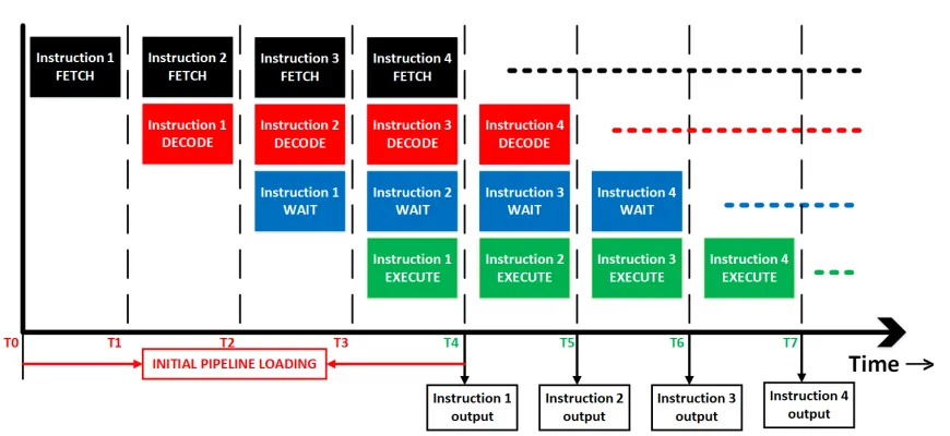
Figure 4.1: Pipeline stages and implementation
are:
1. It takes at least one clock cycle to fetch data from the ROM.
2. The DSP requires one clock cycle to decode the instruction coming from the ROM.
3. Data transfer to and from the RAM also takes at least one clock cycle.
4. Most instructions in the DSP use direct memory access (DMA), hence most of them will have to read data from the RAM.
5. Most instructions are to be executed within a single clock cycle.
Considering all the points mentioned above, the DSP pipeline has been divided into 4 stages. The name and function of each stage is described in Fig. 4.1.
1. The first stage is FETCH, where operand is fetched from the ROM. The program
[image:44.612.90.525.91.291.2]2. The second stage is DECODE, where the fetched instruction is decoded. This stage
is responsible for generating the RAM address and corresponding handshake signals, if necessary.
3. The third stage isWAIT, where the DSP waits for data to be fetched from the RAM,
and feeds the read data into the execution unit. Also, updating AR and ARP is done at this stage.
4. The fourth stage isEXECUTE, where all arithmetic operations are performed by the
DSP.
Fig.4.1.1illustrates how the pipeline works in the DSP for the first 4 instructions. Assuming that the DSP is reset at T0, it is observed that the DSP does not execute the first instruction until T4. However, after T4, for every cycle there will be an output. Hence, technically all single cycle instructions have a latency of 4 cycles, though they just take a single cycle to execute.
4.1.2
Pipeline design for non-branching instructions
The pipelining of non-branching instruction is straight forward for all read instructions. Write instructions however need to be modified slightly because of the way the RAM memory works and DMA design of the DSP.
Fig.4.2 illustrates the pipeline operation for DMA read instructions, where all four instructions are assumed to be DMA read instructions. The steps followed at each pipeline stage of the implementation of DMA read instruction are listed below:
4.1 Pipeline implementation 36
Figure 4.2: Pipeline example for memory read instructions
2. Decode stage: The decode stage here decodes whether the instruction is direct ad-dressing or indirect adad-dressing. It is also responsible to setup the appropriate hand-shake signals for memory read and generate read address after decoding the instruc-tion.
3. Wait stage: In the case of direct addressing, the wait stage does nothing. However, this stage takes care of updating AR and ARP registers for indirect addressing.
4. Execute stage: By this stage, the memory read operation would have finished. Hence, the fetched data is now used by the execution unit to compute. By the end of this cycle, the output is either stored in the Product register or the accumulator, depending on the instruction executed.
[image:46.612.86.520.103.372.2]are DMA write instructions, while the first and fourth are DMA read instructions. The steps followed at each pipeline stage of the implementation of DMA write instruction are listed below:
1. Fetch stage: This stage is the exact same as DMA read fetch stage. Hence, the instruction is read from the ROM and passed on to the decode stage, while incre-menting the value of PC by one for fetching the next instruction.
2. Decode stage: The instruction is decoded, setting up the write address according to direct/indirect addressing. Appropriate handshake signals for memory write are generated.
3. Wait stage: By the time this stage is completed, the appropriate write data needs to be ready. To accomplish this, appropriate changes in the architecture have been made at this stage to shift the output of the results of the fourth cycle of the pre-vious instruction in the case of SAC or store accumulator instruction, in case the previous instruction is an ALU operation. The updating of AR and ARP for indirect addressing also it the responsibility of this stage.
4. Execute stage: During this stage, the memory write operation is performed by the read/write RAM buffer wrapper.
4.1.3
Pipeline design for unconditonal branching instructions
4.1 Pipeline implementation 38
[image:48.612.87.522.253.520.2]During the execution of two-word branch instruction, all stages of the pipeline are stalled while reading the second word, since it is not an instruction. Appropriate changes are made at every pipeline stage to make sure that the second word is not read as an instruction, but stored as jump address.
There are two types of branching instructions, namely conditional and unconditional branching instructions. Unconditional branching instructions are BU (branch uncondi-tional), CALL (call) and RET (return), where branch must always be taken. Conditional branching instructions are where the branching decision is made based on the valuation of a condition.
Figure 4.4 shows a pipeline implementation example of unconditional branch instruc-tion. The steps followed at each pipeline stage of the implementation of unconditional branch instructions are listed below:
1. Fetch stage: The DSP during this stage reads the instruction from the ROM and increments PC by one, just like all other instructions. However, the fetch is stalled in order to read the jump or branch address.
2. Decode stage: The instruction is decoded, and call registers are accordingly modified for call and return instructions, while the jump address is read from the program memory and fed to the PC.
3. Wait stage: As the unconditional instruction has already been executed at this point, this stage does almost nothing. However, for call and return instructions, the stack pointer is stored and restored respectively at this stage.
4.1 Pipeline implementation 40
Figure 4.4: Pipeline example for unconditional branching
4.1.4
Pipeline design for conditional branching instructions
Before looking at the implementation of conditional branching, it is necessary to understand how the instruction works in practice. Since almost all conditional branching instructions rely either on status flags resulting from an ALU operation, or the ALU result itself, timing and data dependency wise, the worst-case scenario of the previous instruction being an ALU operation is assumed before approaching to design the pipeline stages.
[image:50.612.86.532.88.324.2]fetch the next instruction from. In other words, during the second pipeline stage, the PC needs to be updated to the next program address to fetch from. This results in a dilemma, as the branching decision needs to be made at the second stage of the pipeline, however the decision is not available until the fourth stage.
There are two solutions to this problem:
Solution 1: Decide to not take the branch, and make necessary changes if the condition turns out to be true.
Solution 2: Predict the branch, and pay the penalty of two cycles if wrong by making necessary changes in the case of a wrong prediction.
Though solution 2 is a better option and has numerous methods of execution, even the simplest branch predictor requires a lot of additional hardware and planning. To keep the DSP design simple, solution 1 is considering in this design.
Figures4.5and4.6illustrate both cases of the working of pipeline for conditional branch instructions, the first case where the condition evaluates to be false, and the second case where the condition evaluates to be true. In both cases, the first instruction is assumed to be the evaluation instruction, hence the branch/jump condition is evaluated based on its outcome. The second instruction is the conditional branch instruction, while the last two instructions are unconditional instructions.The pipeline plan of action for each stage is listed below:
1. Fetch stage: The DSP during this stage reads the instruction from the ROM and increments PC by one, just like all other instructions. Fetching of the next instruction is stalled to read the jump or branch address.
4.1 Pipeline implementation 42
Figure 4.5: Pipeline implementation example for conditional branch instruction, when condition is false
incremented by one for the pipeline to work smoothly, and not waste any cycles in case the branch evaluates to be false.
3. Wait stage: This stage does performs no task.
[image:52.612.89.527.89.313.2]Figure 4.6: Pipeline implementation example for conditional branch instruction, when condition is true
4.2
Read/write RAM buffer wrapper
DSPs have much higher memory bandwidth and use lot more memory-to-memory instruc-tions, when compared to traditional processors [25]. While most DSPs tackle this problem using small, fast and simple parallel memory banks, it is very difficult to design compilers and the power consumption increases significantly for such DSPs [18]. Since it has been established that data memory access is very important in DSPs, it is crucial to ensure that memory access is quick and effective, while keeping the power consumption low. Hence, both, data and address memories have been clocked at the same speed as the DSP, in an effort to keep the total power consumption low.
[image:53.612.90.527.90.313.2]4.2 Read/write RAM buffer wrapper 44
TMS32010, even though the ISA is almost the same, this problem is not observed in the case of TMS32010. This is mainly because TMS32010 had its memory clocked to at least twice the speed of the DSP itself. This is evident from some of the instructions in its ISA, which have obviously not been implemented in this DSP. A good example for this is the LTA instruction, which featured multiple memory transactions within a single clock cycle. [20]
Section 4.2.1 describes what problems were faced due to clocking the memory at the same speed as the processor, and Section4.2.2describes how the problem has been resolved using the read/write RAM buffer wrapper.
4.2.1
RAM read/write problem description
Looking at the pipeline implementation in the case of data memory or DMA write opera-tions in Section4.1.2, it is observed that write address and handshaking signal generation happens at stage 2 or decode stage, while the write data is sent to the data memory in the next stage, which is stage 3 or the wait stage. However, the RAM requires the address, handshaking signals, along with the data to be written, all within the same cycle. This is not possible with the pipeline design implemented in this paper, since the write data may be computed in last stage of the pipeline of the previous instruction.
Figure 4.7: Read/write RAM buffer wrapper state machine
4.2.2
Design and implementation of read/write buffer wrapper
The wrapper is designed with a simple goal: delay the data memory write operation by a single cycle, while seamlessly providing the correct data whenever necessary. Translating this to a plan of action, the following procedures were followed:
1. For every write operation, store the address and corresponding data.
2. For every read, check the address. If it matches the buffer address, transfer the contents of the buffer data as the output to the DSP. Else, make the necessary arrangements to fetch the data directly from the RAM, and send it to the DSP.
3. For every other write operation following the first, store the buffer data onto RAM and update the buffer address and data with the corresponding new values.
[image:55.612.161.452.107.236.2]4.2 Read/write RAM buffer wrapper 46
1. Read state: Read state is also the idle state. If the read address matches the buffer address register contents, the buffer data is transferred to the DSP. However, if the read address is different from the buffer address register contents, the required data is fetched from RAM and transferred to the DSP within the next clock cycle.
2. Write state: A single bit flag is used to keep track of whether the buffer data has been transferred onto the RAM or not. Every time a new data arrives, if data is present in the data buffer register, it is transferred to the RAM address corresponding to the buffer address, which is retrieved from the buffer address register. This is followed by storing the write address in the buffer address register.
3. RAW state: In the RAW state or read-after-write state, the write data is stored in the buffer data register. Also, all functions in the read state are performed here as well.
Median filter design
Image processing and filtering is an area where DSPs have been used extensively since their invention. In the recent years however, more complex image processing have been handled by GPUs or graphical processsing units mainly due to their hardware parallelism and enormous amount of data required to be processed. However, numerous image filtering applications are still use DSPs, but with multiprocessor type configuration.
Taking a brief look at image data, it is usually represented by the amount of Red, Green and Blue (RGB) colors over a fixed area of a preset number of very small points called pixels. The common representation of a standard dimension image is 24-bit RGB values per pixel, over an area of (720 x 576) pixels. Most simple DSPs are 16-bit fixed-point architectures, hence to handle image data they would require two data words per pixel. Expanding the data word to at least 24-bits hence could result in further applications in image handling and processing.
5.1 Median filter overview 48
works. Section 5.2 discusses the median filter algorithm design and its implementation.
5.1
Median filter overview
Median filters are non-linear digital filters used widely to get rid of salt and pepper noise. The implementation of the median is quite is simple and straight forward. Considering a 3x3 window of pixels of an image, the following steps are followed to find the median:
Step 1: Arrange the pixels one after the other.
Step 2: Rearrange the pixels in an ascending or descending order.
Step 3: Pick the central value of the arranged pixels, which is the fifth pixel in this
case. This will be the median.
While the median filter implementation looks like a simple two-step process, it takes a significant amount of effort to arrange the pixels in ascending or descending order, as every pixel needs to be compared to every other pixel, and this needs to be done sequentially to keep track of the order of their arrangement.
Fig.5.1 illustrates the working of a median filter. In the figure, P1, P2, P3, P4, P5, P6, P7, P8 and P9 are pixel values of the 3x3 window from the image. After step 2, note that the new pixel values P1‘, P2‘, P3‘, P4‘, P5‘, P6‘, P7‘, P8‘ and P9‘ indicated in the figure represent the rearranged pixel values.
5.2
Median filter design and implementation
The median filter algorithm design for the 3×3 pixel window is explained in figure 5.2.
Figure 5.1: Median filter working illustration
[image:59.612.82.527.125.316.2] [image:59.612.87.524.412.640.2]5.2 Median filter design and implementation 50
The implementation of this algorithm on an image is done by moving the 3×3 window
from the top-left corner of the image across all columns, and soon as the median for the first row has been computed, the window is moved to the next row. This is repeated until the last row is computed. Fig. 5.3 illustrates the implementation of algorithm on an image. The first part of the figure shows the 3×3 window placement while computing
Chapter 6
Results
This chapter discusses the results from this project, as well as future work that could be completed.
6.1
Results
The DSP design was synthesized using Synopsys Design Compiler at 180 nm technology nodes from TMSC. Cadence Virtuoso Suite was used for design, debuging and simulation of the design. Table 6.1 gives the synthesis results for the post-scan netlist of the design, when synthesized at 50MHz.
Table 6.1: Synthesis results
Noncombinational area 181298 Area Combinational area 167021 (µm2) Buf/ Inv area 9027
Total cell area 348320 Internal Power 9.4111
Power Switching Power 1.6481
(mW) Leakage Power 1.4210
Total 11.0607 Timing Data arrival time 18.1474
(ns) Slack 1.4799
Chapter 7
Conclusions and future work
7.1
Conclusion
The DSP design has been successfully implemented, verified for the instructions mentioned in Appendix A and synthesized at 50MHz. The design was kept simple, since its ISA and architecture have been based on the TMS32010. Power efficiency was achieved by running the memory at the same speed as the DSP. A median filter algorithm was designed in assembly, simulated at gate-level and verified to work on the DSP within 100 instructions, demonstrating that the enhanced SIMD instructions could be used for median filter compu-tation, hence proving that the DSP is capable of handling simple multimedia applications.
7.2
Future work
filter algorithm described in chapter 5, though successfully implemented, could not be tested with a noisy image due to time constraints. Doing this would demonstrate the capabilities of the DSP, and a comparison of the results with a similar implementation on the TMS32010 would prove the claims presented in the paper.
References
[1] B. Marr, “Big data: 20 mind-boggling facts everyone must read.”
[2] T. Jamil, “Risc versus cisc,”Ieee Potentials, vol. 14, no. 3, pp. 13–16, 1995.
[3] W. P. Hays, “Dsps: Back to the future,”Queue, vol. 2, no. 1, p. 42, 2004.
[4] D. Zuras, M. Cowlishaw, A. Aiken, M. Applegate, D. Bailey, S. Bass, D. Bhandarkar, M. Bhat, D. Bindel, S. Boldo et al., “Ieee standard for floating-point arithmetic,”
IEEE Std 754-2008, pp. 1–70, 2008.
[5] S. W. Smith,The scientist and engineer’s guide to digital signal processing. California
Technical Pub., 1999.
[6] C. Inacio and D. Ombres, “The dsp decision: Fixed point or floating?” IEEE
Spec-trum, vol. 33, no. 9, pp. 72–74, 1996.
[7] S. Smith, Digital signal processing: a practical guide for engineers and scientists,
S. Smith, Ed. Newnes, 2013.
[8] G. Frantz, “Signal core: A short history of the digital signal processor,”IEEE
[9] E. J. Tan and W. B. Heinzelman, “Dsp architectures: past, present and futures,”
ACM SIGARCH Computer Architecture News, vol. 31, no. 3, pp. 6–19, 2003.
[10] A. Abnous and N. Bagherzadeh, “Pipelining and bypassing in a vliw processor,”IEEE
Transactions on Parallel and Distributed Systems, vol. 5, no. 6, pp. 658–664, 1994.
[11] J. Glossner, J. Moreno, M. Moudgill, J. Derby, E. Hokenek, D. Meltzer, U. Shvadron, and M. Ware, “Trends in compilable dsp architecture,” in Signal Processing Systems,
2000. SiPS 2000. 2000 IEEE Workshop on. IEEE, 2000, pp. 181–199.
[12] C. Choo, J. Chung, J. Fong, and S. E. Cheung, “Implementation of texas instruments tms32010 dsp processor on altera fpga,” inGlobal Signal Processing Expo & Conf. San
Jose State University, 2004.
[13] J. L. Hennessy and D. A. Patterson, Computer architecture: a quantitative approach.
Elsevier, 2011.
[14] S. L. Harris and D. M. Harris, Digital Design and Computer Architecture: ARM
Edition. Morgan Kaufmann, 2016.
[15] A. David and H. John, “Computer organization and design: the hardware/software interface,”San mateo, CA: M organ Kaufmann Publishers, vol. 1, p. 998, 2005.
[16] K. Ngan, A. Kassim, and H. Singh, “Parallel image-processing system based on the tms32010 digital signal processor,” IEE Proceedings E (Computers and Digital
Tech-niques), vol. 134, no. 2, pp. 119–124, 1987.
References 58
[18] E. A. Lee, “Programmable dsp architectures. i,” IEEE ASSP Magazine, vol. 5, no. 4,
pp. 4–19, 1988.
[19] G. Araujo, A. Sudarsanam, and S. Malik, “Instruction set design and optimizations for address computation in dsp architectures,” in Proceedings of the 9th international
symposium on System synthesis. IEEE Computer Society, 1996, p. 105.
[20] T. Instruments and P. Strzelecki,TMS32010 User’s Guide. Texas Instruments, 1983.
[21] T. Jain and T. Agrawal, “The haswell microarchitecture-4th generation processor,”
International Journal of Computer Science and Information Technologies, vol. 4, no. 3,
pp. 477–480, 2013.
[22] P. M. Kogge, The architecture of pipelined computers. CRC Press, 1981.
[23] E. A. Lee, “Programmable dsp architectures. ii,”IEEE ASSP Magazine, vol. 6, no. 1,
pp. 4–14, 1989.
[24] E. Lee and D. Messerschmitt, “Pipeline interleaved programmable dsp’s: Architec-ture,” IEEE Transactions on Acoustics, Speech, and Signal Processing, vol. 35, no. 9,
pp. 1320–1333, 1987.
[25] N. H. Weste and D. Harris, CMOS VLSI design: a circuits and systems perspective.
Source Code
I.1
RTL source code
I.1.1
DSP top level module
1 //
////////////////////////////////////////////////////////////////////////////
2 // Author : Shashank Simha 3 // Date : 12/12/2017
4 // U n i v e r s i t y : Rochester I n s t i t u t e o f Technology
5 // D e s c r i p t i o n : This i s a part o f the DSP implemented f o r grad p r o j e c t 6 //
////////////////////////////////////////////////////////////////////////////
7 module DSP_Version1 (
8 r e s e t ,
9 clk ,
10 scan_in0,
11 scan_en,
12 test_mode,
13 scan_out0,
14 SW_pin, Display_pin,
15 DM_out, CEN, wr_data, DM_Addr, DM_in, OEN, // ram_buffer
16 PC, PM_out //rom
17 ) ;
I.1 RTL source code I-2
20 input [ 4 : 0 ] SW_pin; // Four s w i tc h e s and one push−button
21 output [ 7 : 0 ] Display_pin; // 8 LEDs 22
23 input
24 r e s e t , // system r e s e t
25 c l k; // system c l o c k
26
27 input
28 scan_in0, // t e s t scan mode data input
29 scan_en, // t e s t scan mode enable
30 test_mode; // t e s t mode s e l e c t
31
32 output
33 scan_out0; // t e s t scan mode data output
34
35 // ///////////RAM ports /////////////////// 36 output [ 1 4 : 0 ] DM_Addr;
37 output [ 3 1 : 0 ] DM_in; 38 input [ 3 1 : 0 ] DM_out;
39 output reg wr_data, OEN, CEN;
40 // ///////////ROM ports /////////////////// 41 input[ 1 5 : 0 ] PM_out;
42 output reg [ 1 5 : 0 ] PC;
43 // ////////////////////////////// 44
45
46 //−−−−−−−−−−−−−−−−−−−−−−−−−−−−−−−−−−−−−−−−−−−−−−−−−−−−−−−−−−−
47 //−− 1 ISA Parameters
48 //−−−−−−−−−−−−−−−−−−−−−−−−−−−−−−−−−−−−−−−−−−−−−−−−−−−−−−−−−−−
49 parameter [ 7 : 0 ] MPY = 8 'b00000000; // 1 . 50 parameter [ 7 : 0 ] MPYK = 8 'b10100000; // 2 . 51 parameter [ 7 : 0 ] MAC = 8 'h02; // 3 .
69 parameter [ 7 : 0 ] LACK = 8 'b10100001; // 22 . 70 parameter [ 7 : 0 ] LAR = 5 'b11000; // 2 3 . 71 parameter [ 7 : 0 ] LARK = 5 'b11001; // 2 4 . 72 parameter [ 7 : 0 ] LARKH = 5 'b11011; // 2 5 . 73 parameter [ 7 : 0 ] LARP = 8 'b10100011; // 2 6 . 74 parameter [ 7 : 0 ] LDP = 8 'h09; // 2 7.
75 parameter [ 7 : 0 ] LDPK = 8 'b10100100; // 2 8 . 76 parameter [ 7 : 0 ] LT = 8 'h0a; // 2 9.
77 parameter [ 7 : 0 ] LTA = 8 'h0b; // 3 0 . 78 parameter [ 7 : 0 ] LTD = 8 'h0c; // 31 . 79 parameter [ 7 : 0 ] LTP = 8 'h0d; // 3 2 . 80 parameter [ 7 : 0 ] LTS = 8 'h0e; // 33 . 81 parameter [ 7 : 0 ] MAR = 8 'h0f; // 34 . 82 parameter [ 1 5 : 0 ] PAC = 16 'h011F; // 3 5 . 83 parameter [ 1 5 : 0 ] ROVM = 16 'h012F; // 3 6 . 84 parameter [ 2 : 0 ] SAC = 3 'h4; // 3 7 . 85 parameter [ 7 : 0 ] SAR = 5 'b11010; // 3 8 . 86 parameter [ 1 5 : 0 ] SOVM = 16 'h013F; // 39 . 87 parameter [ 7 : 0 ] TBLR = 8 'h11; // 4 0. 88 parameter [ 7 : 0 ] TBLW = 8 'h12; // 4 1. 89 parameter [ 1 5 : 0 ] NOP = 16 'h014F; // 42 . 90 parameter [ 1 5 : 0 ] ZAC = 16 'h015F; // 43 . 91 parameter [ 7 : 0 ] ZALH = 8 'h13; // 4 4. 92 parameter [ 7 : 0 ] ZALS = 8 'h14; // 4 5. 93 parameter [ 1 5 : 0 ] APAC = 16 'h016F; // 46 . 94 parameter [ 6 : 0 ] CMPSIMD = 7 'b0001101; // 47 . 95 parameter [ 7 : 0 ] SUBSIMD = 8 'h16; // 4 8. 96 parameter [ 7 : 0 ] ADDSIMD = 8 'h17; // 4 9. 97 parameter [ 8 : 0 ] BANZ = 8 'h18; // 1 3. 98 parameter [ 1 5 : 0 ] PUSH = 16 'h018F; // 50 . 99 parameter [ 1 5 : 0 ] POP = 16 'h017F; // 51 . 100 parameter [ 1 5 : 0 ] CALL = 16 'h01AF; // 5 2 . 101 parameter [ 1 5 : 0 ] RET = 16 'h019F; // 53 . 102
103 //−−−−−−−−−−−−−−−−−−−−−−−−−−−−−−−−−−−−−−−−−−−−−−−−−−−−−−−−−−−
104 //−− 2 I n t e r n a l r e g i s t e r s (& wires )
105 //−−−−−−−−−−−−−−−−−−−−−−−−−−−−−−−−−−−−−−−−−−−−−−−−−−−−−−−−−−−
106 reg [ 1 5 : 0 ] AR [ 7 : 0 ] ; // 7 A u x i l i a r y R e g i s t e r s o f width 16−b i t s each
107 reg [ 2 : 0 ] ARP, PARP; // 2 R e g i s t e r s to s t o r e current and previous AR p o i n t e r s
108
109 reg [ 7 : 0 ] DPPTR; 110
111 reg [ 3 1 : 0 ] acc, Preg; 112 reg [ 1 5 : 0 ] Treg; 113
114 wire [ 1 5 : 0 ] SR_wire;
I.1 RTL source code I-4
117 reg [ 4 : 0 ] SP; // Stack p o i n t e r 118 reg [ 4 : 0 ] CSP;// Call stack p o i n t e r ;
119 //−−−−−−−−−−−−−−−−−−−−−−−−−−−−−−−−−−−−−−−−−−−−−−−−−−−−−−−−−−
120 //−− 3 P i p e l i n e r e g i s t e r s
121 //−−−−−−−−−−−−−−−−−−−−−−−−−−−−−−−−−−−−−−−−−−−−−−−−−−−−−−−−−−−
122 reg [ 4 : 0 ] sreg2 , sreg3, sreg4; // Used to temporarily S h i f t value between p i p e l i n e s t a g e s
123 reg [ 1 5 : 0 ] JAddr2, JAddr3, JAddr4, JAddr;// Used to temporarily s t o r e Jump Address between p i p e l i n e s t a g e s
124 reg [ 3 1 : 0 ] temp_acc; 125 reg [ 3 1 : 0 ] breg;
126 reg [ 1 5 : 0 ] PAR [ 7 : 0 ] ; // 7 A u x i l i a r y R e g i s t e r s o f width 16−b i t s each
127 reg cnt; //
128 reg JFlag, JFlag_del, JFlag_c, JFlag_uc;
129 reg stall_mc1 , stall_mc2, stall_mc3 , stall_mc4 , s t a l l _ u c;//
130 reg [ 1 5 : 0 ] IR2, IR3, IR4, IR_del;
131 reg J_detect;
132 reg [ 1 5 : 0 ]DM_Addr_reg;
133 //−−−−−−−−−−−−−−−−−−−−−−−−−−−−−−−−−−−−−−−−−−−−−−−−−−−−−−−−−−−
134 //−− 4 Memory c l o c k setup
135 //−−−−−−−−−−−−−−−−−−−−−−−−−−−−−−−−−−−−−−−−−−−−−−−−−−−−−−−−−−−
136 // a s s i g n clk_n <=~c l k ;
137 reg get_DMAddr;
138 139
140 reg [ 3 1 : 0 ] stack [ 3 1 : 0 ] ; // 32 stack r e g i s t e r s 141 reg [ 1 5 : 0 ] c a l l _ s t a c k [ 3 1 : 0 ] ;// 32 c a l l stack r e g i s t e r s 142 reg [ 1 5 : 0 ] call_SR [ 3 1 : 0 ] ; // 32 c a l l SR r e g i s t e r s 143
144
145 reg [ 1 5 : 0 ] alu_opcode, mpy_opcode, next_opcode;
146 //−−−−−−−−−−−−−−−−−−−−−−−−−−−−−−−−−−−−−−−−−−−−−−−−−−−−−−−−−−−
147 //−−−−−−−−−−−−−−−−−−−−−−−−−−−−−−−−−−−−−−−−−−−−−−−−−−−−−−−−−−−
148 //−−−−−−−−−−−−−−−−−−−−−−−−−−−−−−−−−−−−−−−−−−−−−−−−−−−−−−−−−
149
150 reg DM_cnt;
151
152 wire [ 3 1 : 0 ] s1_in; 153 wire [ 3 1 : 0 ] s1_out; 154
155 wire [ 3 1 : 0 ] alu_out; 156
157 wire [ 1 5 : 0 ] mult_2; 158 wire [ 3 1 : 0 ] r e s u l t; 159
160 wire [ 3 1 : 0 ] Preg_wire; 161 reg [ 3 1 : 0 ] s1_in_reg, b u f f; 162 reg [ 1 5 : 0 ] buff_mult_2;
164
165 wire branch_predict;
166 reg check_condition;
167
168 a s s i g n branch_predict = (IR4[15:0]==BZ) ? ( (acc==0)? 1 : 0 ) : 169 (IR4[15:0]==BV) ? ( (SR[15]==0) ? 1 : 0 ) : 170 (IR4[15:0]==BNZ) ? ( (acc!=0) ? 1 : 0 ) : 171 (IR4[15:0]==BLZ) ? ( (acc< 0) ? 1 : 0 ) : 172 (IR4[15:0]==BLEZ) ? ( (acc<=0)? 1 : 0 ) : 173 (IR4[15:0]==BGEZ) ? ( (acc>=0)? 1 : 0 ) : 174 (IR4[15:0]==BGZ) ? ( (acc> 0) ? 1 : 0 ) :
175 ( (IR4[15:8]==BANZ) && (IR4[6:0]==0) ) ? ( (AR[ARP]==0)? 1 : 0 ) :
176 0 ;
177
178 a s s i g n DM_Addr= (get_DMAddr) ? (IR2[ 7 ] == 1? AR[ARP] [ 1 4 : 0 ] : {DPPTR, IR2
[ 6 : 0 ] } ) :
179 (updated_AR) ? AR[ARP] [ 1 4 : 0 ] :
180 DM_Addr_reg;
181
182 a s s i g n mult_2= ( (IR4[15:8]==MAC) | | (IR4[15:8]==MPY) ) ? buff_mult_2:
183 (IR4[15:8]==MPYK) ? {8 'd0, IR4[ 7 : 0 ] } :
184 0 ;
185
186 a s s i g n DM_in = (IR4[ 1 5 : 1 3 ] == SAC) ?
acc :
187 (IR4[ 1 5 : 1 1 ] == SAR) ?
AR[IR4[ 1 0 : 8 ] ] :
188 32 'h0;
189
190 a s s i g n s1_in = ( (IR4[15:8]==MAC) | | (IR4[15:0]==SPAC) | | (IR4[15:0]==APAC) ) ?
Preg:
191 ( (IR4[15:8]==OR) | | (IR4[15:8]==XOR) | | (IR4[15:8]==SUBS) | | (IR4
[15:8]==AND) | | (IR4[15:8]==SUBSIMD) | | (IR4[15:8]==ADDSIMD) | | (IR4[15:9]==CMPSIMD)
192 | | (IR4[15:8]==LTA) | | (IR4[15:8]==LTS) | | (IR4[15:13]==SUB) | | (
IR4[15:13]==ADD) | | (IR4[15:13]==LAC) | | (IR4[15:13]==SAC) ) ?
s1_in_reg:
193 0 ;
194 195
196 //−−−−−−−−−−−−−−−−−−−−−−−−−−−−−−−−−−−−−−−−−−−−−−−−−−−−−−−−−−−
197 //−− 5 I n s t a n t i a t i o n o f components
198 //−−−−−−−−−−−−−−−−−−−−−−−−−−−−−−−−−−−−−−−−−−−−−−−−−−−−−−−−−−−
199 m u l t i p l i e r m1 ( .scan_in0 (scan_in0) ,
200 .scan_out0 (scan_out0) ,
201 .scan_en (scan_en) ,
202 .test_mode (test_mode) ,
I.1 RTL source code I-6
204 .b (mult_2) ,
205 .ov (SR[ 1 5 ] ) ,
206 .product (Preg_wire) ) ;
207
208 // S h i f t s input operand
209 s h i f t e r _ i n p u t s1 ( .scan_in0 (scan_in0) ,
210 .scan_out0 (scan_out0) ,
211 .scan_en (scan_en) ,
212 .test_mode (test_mode) ,
213 .s h i f t _ i n (s1_in) ,
214 .opcode (alu_opcode) ,
215 .shift_out (s1_out) ) ;
216
217 ALU alu1 ( .scan_in0 (scan_in0) ,
218 .scan_out0 (scan_out0) ,
219 .scan_en (scan_en) ,
220 .test_mode (test_mode) ,
221 //
222 .a (acc) ,
223 .b (s1_out) ,
224 .opcode (alu_opcode) ,
225 .r e s u l t (alu_out) ,
226 .carry (SR_wire[ 1 5 ] ) ,
227 .negative (SR_wire[ 1 4 ] ) ,
228 .ov (SR_wire[ 1 3 ] ) ,
229 .zero (SR_wire[ 1 2 ] ) ,
230 .carry_2 (SR_wire[ 1 1 ] ) ,
231 .negative_2 (SR_wire[ 1 0 ] ) ,
232 .ov_2 (SR_wire[ 9 ] ) ,
233 .zero_2 (SR_wire[ 8 ] ) ,
234 .carry_3 (SR_wire[ 7 ] ) ,
235 .negative_3 (SR_wire[ 6 ] ) ,
236 .ov_3 (SR_wire[ 5 ] ) ,
237 .zero_3 (SR_wire[ 4 ] ) ,
238 .carry_4 (SR_wire[ 3 ] ) ,
239 .negative_4 (SR_wire[ 2 ] ) ,
240 .ov_4 (SR_wire[ 1 ] ) ,
241 .zero_4 (SR_wire[ 0 ] )
242 ) ;
243
244 // S h i f t s output operand
245 s hifte r_o u t pu t s2 ( .scan_in0 (scan_in0) ,
246 .scan_out0 (scan_out0) ,
247 .scan_en (scan_en) ,
248 .test_mode (test_mode) ,
249 .s h i f t _ i n (alu_out) ,
250 .opcode (next_opcode) ,
251 .shift_out (r e s u l t) ) ;
253 //−− 6 Code s t a r t s here . . . .
254 //−−−−−−−−−−−−−−−−−−−−−−−−−−−−−−−−−−−−−−−−−−−−−−−−−−−−−−−−−−−
255 always@ (posedge c l k or posedge r e s e t)
256 begin
257 i f(r e s e t)
258 begin
259 PC<= 16 'h0;
260 AR[ 0 ] <= 16 'h0;AR[ 1 ] <= 16 'h0;AR[ 2 ] <=16'h0;AR[ 3 ] <=16'h0; 261 AR[ 4 ] <= 16 'h0;AR[ 5 ] <=16'h0;AR[ 6 ] <=16'h0;AR[ 7 ] <=16'h0;
262 stall_mc1 <