Implementation of AES Using Xilinx System
Generator
B.Satyanarayana, Dr M.Srinivasan
Department of ECE, Sri Satya Sai University of Technology & Medical Science, Sehore, Bhopal,
Madhya Pradesh, India.
Department of ECE, Sri Satya Sai University of Technology & Medical Science, Sehore, Bhopal,
Madhya Pradesh, India.
ABSTRACT: In this paper presents a resource efficient reconfigurable hardware implementation of AES algorithm using HLL approach on FPGA for rapid development. In this work, we use an approach to directly map the design described in a high level package i.e. System Generator on FPGA platforms. This approach is ideal for Encryption functions where the development of data-path architectures can easily be done to provide bit and cycle accurate models. Our approach fills the gap between performance and flexibility by efficiently applying re-configurability. We use primitive level approach and customize all the operations our design by effectively utilizing conventional blocks of Xilinx System Generator to get optimum performance in terms of speed and area. This approach enables us to minimize critical paths in design and increase the overall frequency of design especially for MixColumn and SubByte transform. Our design shows best performance in terms of speed and area as compared with any other software and hardware/software co-design implementation counterparts.
KEYWORDS: AES, System Generator, FPGA, Cryptography
I. INTRODUCTION
In the era of this modern world, secrecy and security are the major concerns which should be kept in mind with respect to digital computer systems. Cryptography provides solutions regarding fool proof secrecy, security, and reliability of given information. It is keeping its vital function in different applications which includes online banking system, Cellular networks, computer hardware emulations, medical imaging, software defined radios, bioinformatics and wireless communication etc. Reconfigurable platform like FPGA are the best for implementation of cryptographic algorithms. These platforms are reconfigurable to provide time and cost effective solutions as compared to Application Specific Integrated Circuit (ASIC). A reconfigurable platform provides improved performance than software implementations and can also be reconfigured on the fly to store the updated encryption standard. In recent years, digital hardware design seems to be more similar to the software design, driven by the increased complex design, time-to-market anxiety and demand for an effective participation between various project teams. Platform-based design has become appropriate for IC design projects in this digital world. To minimize the algorithmic process time in term of plenty of data, it is very much inevitable to adopt and implement the algorithm of hardware, despite the fact that software implementation can only meet the requirement of low cost for users. In order to attain a balance between the cost and time, an efficient method must be explored and implement for various combinations of hardware and software to realize algorithmic best solutions of different requisite. In this work we focus on the efficient and well organized implementation of AES architecture on FPGA using HLL approach i.e. Xilinx System Generator. The proposed FPGA platform for the implementation of this work is Virtex-5 FPGA from Xilinx. HLLs provide a better way to achieve the high-performance in reconfigurable computing to implement any design in hardware. It provides a great deal of functional abstraction and develops highly parallel systems. High level language tool automatically maps the model design to efficient hardware implementation.
architecture using Xilinx System Generator. In section – 5, the verification of design and validity of results are discussed and presents the implementation results of proposed design. The conclusion of the work is given in section – 6.
II. LITERATURE SURVEY
After the approval of AES in 2001, it has been implemented on many different platforms including hardware, software and high level language tools. In this literature we only focus on high level language based implementations of AES related to our work. A large number of AES high level language implementations have been done. Whereas, the earlier implementations mainly focused on the performance criterion but not the time constraints and the flexibility of the designs.
Most recently adopted embedded systems design methodology prototypes a target design in a high-level languages such as C, Handel-C, System C and Impulse C. Most of them translate the design manually into an HDL code that can be prolonged and error-prone, thus reduces the flexibility of a prototype. Other high-level languages that can directly translate the design are too time-consuming. Mostly implementations are focused on software and hardware-based platforms, both have their own pros and cons. Software-based implementations provide cost effective solutions and reduced Time-to-Market but at the cost of performance. Whereas hardware solutions are better in terms of performance but cost of the design and Time-to- Market increases to great extend. High-level language is the platform that provides the features in-between the two. In this study, we have tried to enhance the performance of high-level package by applying some efficient optimization techniques in the design and integrating it with the hardware platform FPGA.
M. Mali et al. implemented AES using high-level design language Handel-C on Celoxica RC1000 development board and Celoxica DK development suite. It runs at the frequency of 74.4 MHz for an external data storage unit. While, in M. Askar et al. presented AES implementation using System C tool and System Crafter tool to translate the System C descriptions into hardware. It takes 153 machine cycles to process 128-bit data. In M. Lukowiak et al. described the AES architecture with data-path of 32-bit using different environment such as Impulse C, C-to-FPGA programming model and Compilation engine to introduce rapid prototyping of digital hardware. The relative performance using Impulse C achieves a speedup of 128.6 times as compared to other software implementations while in D. Osvik et al. has given the AES-128 encryption architecture by targeting not only the low-end processors such as 8-bit AVR microcontroller and 32-bit ARM microprocessor but also on high performance NVIDIA and cell broadband processing engine. On 8-bit AVR microcontroller it offers the frequency of 124.6 cycles/byte while on 32-bit ARM microprocessor it results in the frequency of 34 cycles/byte. The AES architecture is designed to reduce the required number of clock cycles during encryption and decryption using these targeted platforms. In T. Babu et al. reported the hardware together with high-level design tools realization. They implemented the AES algorithm using custom instruction method provided by ARM 7 with Keil platform. Hasamnis et al. has also presented the high-level design architecture for AES implementation where the algorithm is controlled through C-code written in NIOS II IDE that requires 21731020 CPU Cycles to complete the simulation. Bos et. al reported two 128-bit AES implementations on NVIDIA graphics processing units (GPUs) and the Cell broadband engine. The GPU implementation delivers the throughput of 0.17 cycles per byte for encryption module and the Cell broadband engine offer the speed of 11.7 cycles per byte. In Biglari et al present 128-bit pipeline architecture of AES on Maestro platform. This work presents tightly coupled encryption and round key generation modules in the main encryption module that enables the design to reach a throughput of 12.8 Gbps and runs at the speed of 100MHz. Similarly Mourad et al presents the methodology which maps the AES design described in a high level language, Handel-C, to FPGA for low area consideration. This design reported 437 slices for encryption and offers the throughput of 1.716 Gbps.
III. ADVANCED ENCRYPTION STANDARD
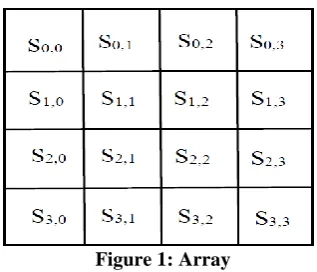
bytes of data arranged in a 4 x 4 array of bytes with four rows and four columns called the state, and is treated as input for AES algorithm as depicted in Figure 1.
Figure 1: Array
AES-128 algorithm comprises of ten rounds and each round further consists of four basic byte-oriented transformations i.e. ShiftRow, SubByte, MixColumn and AddRoundKey except the last round where the MixColumn transformation is eliminated. An initial round is added at the start-up which comprises of only AddRoundKey.
IV. IMPLEMENTATION
Iterative and pipelined architectures are the two basic reconfigurable architectures that are commonly used for the implementation of encryption functions depending on type of application ranging from low to high speed. In this work we adopted pipelined architecture to implement AES encryption function in order to get best possible results in term of throughput. Further we have used the HLL approach to directly map our design on FPGA. In addition, our design is not device-specific; System Generator is highly scalable and can synthesis a design to different FPGA chips that leads to more flexible and fast design.
The block diagram of our full 128-bit AES pipelined architecture is shown in Figure 2, where each round is implemented separately in hardware by enclosing the four transformations as subsystems except in the last round where MixColumn transform has been eliminated. Initial round consists of only AddRoundKey transformation where input data is XORed with the initial Round Key value. Registers are placed at the end of each round forming hierarchical stages within each round of the algorithm. Each 128-bit transform; SubByte, MixColumn, AddRoundkey consists of four parallel copies of 32-bit modules. The detailed implementation and optimization of each is as follows:
Before applying the 32-bit data to each port of the Dual port RAMs for lookup, we first extract 8-bit data from 32-bit input. Because each RAM is able to lookup 8-bit data and we cannot apply the 32-bit data directly to Dual port RAMs. So for this we have used 32-bit to 8-bit conversion block. We can extract our desired 8 bit data by using the slice blocks. But this approach is not efficient in term of resource as it will require numerous slice resources. Therefore we redesigned this block by using custom logic in which we have used the right and left shift methodology to extract 8 bit data which helped us to save resources up to 1700 slices. The detail of 32-bit to 8-bit conversion module is shown in Figure 5. The Shift Row transformation is also implemented within the same SubByte block to save the resources. This is done simply by rearranging the wires according to the shifted data as marked by red box in Figure 4 and applied directly to the RAMs.
In both multipliers in order to satisfy the irreducible condition, the shifted data is XORed with the constant “27” (dec) in hex it is “1b”. The mod 27 must be applied on the results of the multiplication in order to get the number within the range of 255. The MCode block is then designed to select the multiplication result “x” or “y”, which is less than 255. It is programmed by the following code.
AddRoundKey transformation receives 16 bytes of data from MixColumn and performs XORing with the Round Keys. Round Keys are taken from FIPS-197, converted to decimal numbers and are provided on the fly in the form of constants.
Result outputs and behavior of design is verified by giving the pre-defined test vectors defined in AES FIP-197 against standard AES output for testing and validation. Each module is implemented and validated individually. The functionality of each step is tested and verified one by one. Then the verification of output of each round is performed and validated the results after combining all the rounds in the main module.
V. RESULTS
Hardware implementation results are targeted for Xilinx Virtex-6 xc6vsx315t-3ff1156 FPGA. The design has been implemented using Xilinx System Generator tool in MATLAB to generate verilog code (.v file) along with test bench are finally synthesized and simulated using Xilinx ISE Foundation 13.1 and Mentor Graphic ModelSim, respectively. 128-bit AES pipeline architecture occupies 80 BRAM’s for the implementation of SubByte and utilized 380 Slices for the remaining logic. The design operates on maximum frequency of 288.19MHz and offers high throughput of 36.864 Gbps as compared to previously reported designs.
Table 1 details the comparison results of previous AES implementations using HLL on different platforms. Parameters chosen for comparison are platform, to clearly indicate different high level implementation platforms, Data-path to indicate numbers of bit simultaneously processed by design. Operating frequency indicates maximum operational frequency of design and throughput to indicate performance of design.
It’s evident from Table 1 that our performance results of proposed architecture gives better resource utilization and offers greater operating frequency as compared to all other previously reported high-level language tool implementations of AES. Mali et al presents 128-bit AES implementation on Handle-C environment. This design operates at the maximum frequency of 74.4MHz and offers throughput of 7.76(Mbit/s). Askar et al. presented 128-bit AES implementation using System C tool and System Crafter tool to translate the System C descriptions into hardware. It takes 153 machine cycles to process whole data and throughput of 90(Mbit/s). It reported 178 numbers of occupied slices for MixColumn and 197 number of slices for the implementation of Shift Row, whereas our approach gives 380 slices for the whole architecture of AES. Osvik et al previously reported 8-bit AES implementation on AVR and 32-bit AES architecture on ARM platform that operates on the frequency of 124.6 cycles/byte and 34 cycles/byte respectively. Babu et al implemented 128-bit architecture of AES using custom instruction method provided by ARM 7 with Keil platform. Hasamnis et al. has given the high-level design architecture for 128-bit AES implementation where the algorithm is controlled through C-code written in NIOS II IDE that operates on frequency of 217.31020M Cycles. Next, Bos et al reported the 128-bit AES implementation on NVIDIA graphics processing units (GPUs) and the Cell broadband engine. The GPU implementation delivers the throughput of 0.17 cycles per byte for encryption module and the Cell broadband engine offer the speed of 11.7 cycles per byte. In Biglari et al, the 128-bit pipeline architecture of AES is given on Maestro platform. This work presents tightly coupled encryption and round key generation modules in the main encryption module that enables the design to reach a throughput of 12.8 Gbps and runs at the speed of 100MHz. At the end, Mourad et al presents the methodology which maps the AES design described in a high level language, Handel-C, to FPGA for low area consideration. This design reported 437 slices for encryption and offers the throughput of 1.716 Gbps. All the implementations discussed above are not efficient enough for high speed applications as effective frequency of these designs ranges from 34 to 153 machine cycles while our design frequency is 288.19MHz. So, it is concluded that this design is faster than the other reported implementation of AES. In addition, the design utilized minimum number of resources i.e. 380 slices and offers high throughput of 36.864 Gbps as compared to previous one.
VI. CONCLUSIONS
In this work we present efficient implementation of AES in term of area and speed using High Level Language tool. Our methodology not only reduces the overall resource utilization but also provide good enough clock frequency. It provides the user friendly design for Matlab users with very short development time and better performance as compared to any software and hardware-software co-design implementations. The important feature of this work is that so far no any implementation of AES has been reported on Xilinx System Generator.
REFERENCES
1. M. Mozaffari-Kermani, A. Reyhani-Masoleh, "Efficient and High-Performance Parallel Hardware Architectures for the AES-GCM," IEEE Transactions on Computers, vol. 61, no. 8, pp. 1165-1178, Aug. 2012.
2. E. El-Araby, Saumil G. Merchant, T. El-Ghazawi, "A Framework for Evaluating High-Level Design Methodologies for High-Performance Reconfigurable Computers," IEEE Transactions on Parallel and Distributed Systems, vol. 22, no. 1, pp. 33-45, Jan
3. Y. Wang, Y. Ha, "FPGA-Based 40.9-Gbits/s Masked AES with Area Optimization for Storage Area Network", Circuits and Systems II: Express Briefs, IEEE Transactions, vol.60, no.1, pp.36-40, Jan 2013.
4. D. Osvik, J. Bos, D. Stefan and D. Canright, “Fast Software AES Encryption”, FSE'10 Proceedings of 17th International Conference on Fast Software Encryption, pp 75-93, 2010.
5. T. Babu, K. Murthy and G. Sunil, “AES Algorithm Implementation using ARM Processor”, 2nd International Conference and workshop on Emerging Trends in Technology Proceedings published by IJCA, 2011
6. M. Hasamnis, P. Jambhulkar and S. Limaye, “Implementation of AES as a Custom”, Advanced Computing: An International Journal (ACIJ), vol.3, No.4, July 2012.
FIPS-197, “Federal Information Processing Standards Publication FIPS-197, Advanced Encryption Standard (AES)”
http://csrc.nist.gov/publications/fips/fips197/fips-197.pdf, October 1999
7. N.Anitha Christy and P.Karthigaikumar, “FPGA Implementation of AES Algorithm using Composite Field Arithmetic”, ICDCS, pp. 713-717, 2012.
8. FIPS-197, “Federal Information Processing Standards Publication FIPS-197, Advanced Encryption Standard (AES)”
http://csrc.nist.gov/publications/fips/fips197/fips-197.pdf, October 1999
9. J. Bos, D. Osvik, D. Stefan, “Fast Implementations of AES on Various Platforms”, IACR Cryptology ePrint Archive, vol. 501, 2009.
10. M. Biglari, E. Qasemi, B. Pourmohseni, "Maestro: A high performance AES encryption/decryption system", CADS, 17th CSI International Symposium, pp.145-148, 30-31 Oct. 2013.
![2 [5 Bromo 1 (3 chlorobenzyl) 2 methyl 1H indol 3 yl]acetic acid](data:image/gif;base64,R0lGODlhAQABAIAAAP///wAAACH5BAEAAAAALAAAAAABAAEAAAICRAEAOw==)