Compact Filtering Power Divider Based on Half Mode Substrate
Integrated Waveguide
Ali-Reza Moznebi and Kambiz Afrooz*
Abstract—In this paper, a compact filtering power divider (PD) based on half mode substrate integrated waveguide (HMSIW) is presented. The proposed structure is realized by etching slots on the top layer of the HMSIW PD. Accordingly, two resonators are embedded in each patch, as a second order filter. The slots dimensions are obtained by the relationship between them and the extracted external quality factor and coupling coefficient. A good agreement between the simulated and measured results is reported. The measured 3 dB fractional bandwidth is 25% (6.3–8.1 GHz). The maximum insertion loss is 0.9 dB, and the return loss is above 20 dB in the passband. This design has the advantages of low insertion loss, improved out-of-band rejection, compact size, controllable bandwidth, and high selectivity.
1. INTRODUCTION
Conventional waveguides are extensively used in many microwave and millimeter-wave systems such as power dividers (PDs) and high Q filters because of their high power capacity and low loss [1, 2]. However, their applications are limited due to large volume and high cost [3]. Recently, substrate integrated waveguide (SIW) structure has been introduced [4, 5]. An SIW is arranged by two rows of metallic via holes in a planar substrate having the benefits of the conventional waveguides, compactness in size, low cost, and easy integration with planar circuits [6]. The size of an SIW is relatively large. The concept of the half mode substrate integrated waveguide (HMSIW) has been presented in [7]. In this configuration, a bisecting plane is inserted along the magnetic wall. Compared to an SIW, the HMSIW solution allows a size reduction about 50%, as shown in Figure 1.
Bandpass filters can be used for frequency selection and suppression of unwanted bands. In the past few years, increased attention has been paid to the implementation of bandpass filters with the SIW technique [8, 9]. In [8], a dual-band SIW resonator with Sierpinski fractal geometry is proposed. This paper shows an interesting technique to reduce the size of the SIW structure. However, this design has the disadvantage of narrow operation bandwidth due to the resonant nature of its configuration. In [9], a HMSIW filter is introduced, and compact size and controllable bandwidth are obtained. Newly, the combination of the power dividing and filtering functions into a single device is taken into consideration. The combination of both functionalities provides a circuit with benefits of low loss, low cost, and compact size. Several PDs based on SIW and HMSIW have been investigated [10–17]. However, the proposed circuits in [10–14] do not include the bandpass filtering response, which restricts their applications in practical systems. In [15], a multilayer SIW PD with bandpass-filtering response is reported. To achieve bandpass response, four inductive posts are added to the multilayer SIW PD. However, this kind of power divider has the disadvantages of large size and narrow operating bandwidth. An out-of-phase filtering PD using a rectangular SIW cavity is proposed in [16]. This circuit uses magnetic coupling by via-hole coupling window and has large size. In [17], a PD integrated with SIW and defected ground
Received 8 April 2016, Accepted 30 June 2016, Scheduled 12 July 2016 * Corresponding author: Kambiz Afrooz ([email protected]).
x
z y
h
Via hole
W
s d
(a)
x
z y
h
Via hole
s d
W 2
Equivalent magnetic wall
(b)
Figure 1. Configuration of a: (a) SIW structure; (b) HMSIW structure.
structures (DGS) techniques is presented. The reported filtering PDs in [15–17] are not proper to design at high frequencies due to the limitation of via-holes fabrication [18].
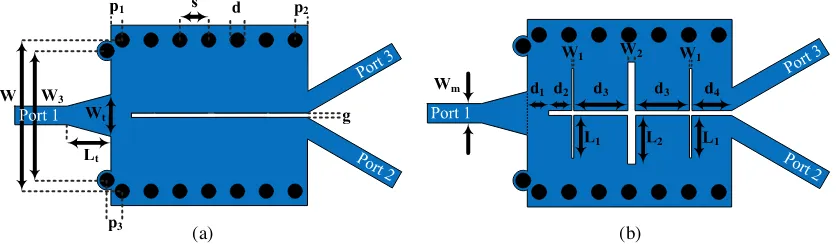
In this paper, an HMSIW PD prototype with a bandpass filter response is designed, simulated, and fabricated. A part of the HMSIW between two rectangular slots is considered as a resonator [9]. Here, two resonators are embedded by etching three rectangular slots on the top layer of each patch. The coupled resonators give the bandpass function. This design has the advantages of low insertion loss, improved out-of-band rejection, compact size, controllable bandwidth, and high selectivity. In this structure, the bandwidth can be controlled by the transverse slots. Figure 2 shows the configuration of the HMSIW PD and proposed filtering HMSIW PD. The paper is organized as follows: Section 1, the introduction; Section 2, the design procedure and results of the HMSIW PD; Section 3, the design procedure and results of the filtering HMSIW PD; Section 4, the conclusion.
`
3
t t
1 2
3
(a)
`
1 2 1
1 2 1
1 2 3 3 4
m
(b)
Figure 2. Configuration of the: (a) HMSIW PD; (b) proposed filtering HMSIW PD.
2. HALF MODE SUBSTRATE INTEGRATED WAVEGUIDE POWER DIVIDER
2.1. Design Procedure
The methodology in this section is divided into two steps. Step 1: calculating the basic SIW parameters. Step 2: determining the taper-via transition parameters.
The dominant mode of this structure is TE10. By using the formula obtained in [20], the equivalent width of the SIW (Weff) is equal to:
Weff =W −1.08d 2
s + 0.1 d2
W (1)
The cut-off frequency of the SIW can be calculated by the following formula [21]:
fc10=
c
2Weff√μrεr (2)
In Equations (1) and (2), W is the width of the SIW,dthe diameter of the vias, sthe distance between the center of two adjacent vias, c the light velocity in vacuum, εr the relative permittivity of the substrate, and μr the relative permeability of the substrate. For better performance of the circuit, d and sare limited as follows [22]:
s
d ≤2 (3)
In the input, a microstrip-to-SIW transition is used [23]. It features two vias, which have the same diameter as the SIW vias and are located symmetrically at both sides of the microstrip taper. The taper-via transition parameters can be calculated as:
Lt = 0.2368λg MS
Wt = Wm+ 0.1547W (4)
p3 = 0.6561s
W3 = 0.8556W
where Wm is the width of 50 Ohm microstrip line and λgMS the guided wavelength of microstrip line calculated at the center frequency:
λgMS = √λg0
εreff (5)
where εreff refers to the effective dielectric constant of the microstrip line and λg0 the wavelength in free space. To achieve the HMSIW PD, the SIW which has the highpass characteristic is divided into two HMSIWs.
3 4 5 6 7 8 9 10 11 12 13 14 15 16 17 -40
-35 -30 -25 -20 -15 -10 -5 0
Frequency (GHz) S - Parameter (dB) S
11
S
21
S
31
2.2. Results
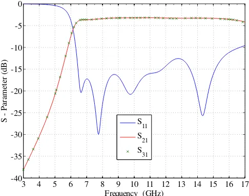
The HMSIW PD is simulated on a single layer Rogers RO4003C substrate with a thickness, relative permittivity, and loss tangent of 0.8128 mm, 3.55, and 0.0027, respectively. The simulated results of this PD are shown in Figure 3. In the aforementioned HMSIW PD, the return loss is greater than 15 dB over 6.45 to 11.75 GHz (fractional bandwidth of 58%), and the maximum insertion loss is 0.9 dB in the passband.
3. FILTERING HALF MODE SUBSTRATE INTEGRATED WAVEGUIDE POWER DIVIDER
3.1. Design Procedure
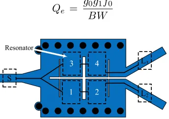
The mentioned HMSIW PD is transformed to the filtering HMSIW PD to improve the performance of the circuit. To design the filtering HMSIW PD, the adjusted transverse slots are added to the HMSIW PD. Each part of the HMSIW between two transverse slots is considered as a resonator. Here, two resonators are embedded by etching three rectangular slots on the top layer of each patch. The coupled resonators give the bandpass function. The coupling scheme of this filtering PD is illustrated in Figure 4. A bandpass filter is designed to meet the specifications: the center frequency f0 = 7 GHz and 3 dB bandwidth BW = 1.2 GHz with 0.5 dB passband ripple. This design consists of two steps.
Step 1: The external quality factor (Qe) and coupling coefficient between the two resonators (K12) can be evaluated by using the following relations [24]:
Qe = g0g1f0
BW (6)
`
Figure 4. Coupling scheme of the proposed filtering HMSIW PD.
3 4 5 6 7 8 9 10 11 12 13 14 15 16 17
-45 -40 -35 -30 -25 -20 -15 -10 -5 0
Frequency (GHz)
S - Parameter (dB)
S
11
S
21
S
31
K12 = BW f0√g1g2
(7)
where g0,g1,g2, and g3 are Chebyshev low-pass prototype element values. The evaluated value of Qe is 8.18, andK12 is 0.172. The ideal response for this filter is shown in Figure 5.
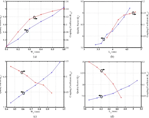
Step 2: The width and length of the rectangular slots are tuned by a 3D EM simulator to determine the relationship between the physical dimensions of the slots and Qe and K12. Qe and K12 can be calculated by [24]:
Qe = 2f0
BW (8)
K12 =
f12−f22
f12+f22 (9)
where f1 and f2 represent the higher and lower resonant frequencies, respectively. Figure 6 shows the external quality factor and coupling coefficient between the two resonators versus the width and length of the rectangular slots. The external quality factor and coupling coefficient can be increased by
0.1 0.2 0.3 0.4 0.5 0.6
8 8.2 8.4 8.6 8.8 9 9.2 W
1 (mm)
Quality Factor (Q
e
)
0.1 0.2 0.3 0.4 0.5 0.60.04
0.06 0.08 0.1 0.12 0.14 0.16
Coupling Coefficient (K
12
)
(a)
3 3.5 4 4.5 5
7.5 8 8.5 9 9.5 L
1 (mm)
Quality Factor (Q
e
)
3 3.5 4 4.5 50
0.05 0.1 0.15 0.2
Coupling Coefficient (K
12
)
(b)
0.4 0.5 0.6 0.7 0.8 0.9 1 1.1
7.5 8 8.5 9
Quality Factor (Q
e
)
0.4 0.5 0.6 0.7 0.8 0.9 1 1.10
0.05 0.1 0.15
W
2 (mm)
Coupling Coefficient (K
12
)
(c)
3.8 4 4.2 4.4 4.6 4.8 5 5.2
5 7.5 10 12.5 15 L
2 (mm)
Quality Factor (Q
e
)
3.8 4 4.2 4.4 4.6 4.8 5 5.20
0.05 0.1 0.15 0.2
Coupling Coefficient (K
12
)
(d)
Table 1. Dimensions of the HMSIW PD and filtering HMSIW PD.
W 14.65 (mm) L2 4.58 (mm) p1 1.11 (mm) W1 0.2 (mm) Lt 4.24 (mm) p2 1.22 (mm)
W2 0.75 (mm) d1 2 (mm) p3 1.04 (mm) W3 12.56 (mm) d2 2.15 (mm) s 2.79 (mm) Wt 4.06 (mm) d3 5.02 (mm) d 1.45 (mm) L1 4 (mm) d4 3.74 (mm) g 0.4 (mm)
increasing W1 and L1, as shown in Figure 6(a) and Figure 6(b). Moreover, Qe can be increased, and K12 can be decreased by increasing W2 and L2, as shown in Figure 6(c) and Figure 6(d). It should be noted here that the extracted Qe and K12 from Figure 5 are 8.2 and 0.126, respectively. Table 1 exhibits the dimensions of the HMSIW PD and filtering HMSIW PD.
3.2. Results
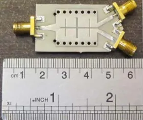
The filtering HMSIW PD is fabricated on a single-layer Rogers RO4003C substrate with a thickness, relative permittivity, and loss tangent of 0.8128 mm, 3.55, and 0.0027, respectively. A photograph of the proposed filtering HMSIW PD is depicted in Figure 7. The fabricated circuit is tested by the network analyzer “Rohde & Schwarz, zvk”. Figure 8 indicates the simulated and measured S11, S21, and S31.
Figure 7. Photograph of the fabricated filtering HMSIW PD.
3 4 5 6 7 8 9 10 11 12 13 14 15 16 17
-55 -50 -45 -40 -35 -30 -25 -20 -15 -10 -5 0
Frequency (GHz)
S - Parameter (dB)
3 4 5 6 7 8 9 10 11 12 13 14 15 16 170
5 10 15 20 25 30 35 40 45 50 55
Radiation Loss (%)
S
21 Measured
S
21 Simulated
S
31 Measured
S
31 Simulated
S
11 Measured S11 Simulated
The measured 3 dB fractional bandwidth is 25% (6.3–8.1 GHz). The maximum insertion loss is 0.9 dB, and the return loss is above 20 dB in the passband. Moreover, the out-of-band rejection band is over 25 dB from 9.8 GHz to 13.7 GHz. The simulated and measured results are in good agreement. There is a slight frequency shift of approximately 2%, and the maximum simulated insertion loss is about 0.3 dB better than the measured insertion loss. Some slight differences between the simulated and measured results are mainly caused by the insertion loss of SMA connectors and the tolerances of the dielectric constant. In Figure 8, the radiation loss is defined as:
Rr= 1−S11S11∗ −S21S21∗ −S31S31∗ (10)
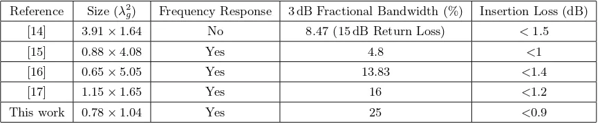
In this figure, the radiation loss (Rr) is less than 4.9% under the conditions of lossless metal and substrate. This parameter guarantees that the produced radiation is negligible. In Table 2, a comparison between the presented filtering HMSIW PD and the other PDs is summarized. In this table, the advantages in fractional bandwidth and insertion loss are very obvious. Furthermore, the proposed filtering HMSIW PD has a size of 1.04×0.78λ2g, which is much more compact than that in [14–17]. Also, compared with the reported circuit in [17], a size reduction of 42% is achieved.
Table 2. Comparison with other PDs.
Reference Size (λ2g) Frequency Response 3 dB Fractional Bandwidth (%) Insertion Loss (dB)
[14] 3.91×1.64 No 8.47 (15 dB Return Loss) <1.5 [15] 0.88×4.08 Yes 4.8 <1 [16] 0.65×5.05 Yes 13.83 <1.4 [17] 1.15×1.65 Yes 16 <1.2 This work 0.78×1.04 Yes 25 <0.9
4. CONCLUSION
A compact filtering PD based on HMSIW has been presented. The bandpass filtering response is implemented by etching slots on the top layer of the HMSIW PD. The slots dimensions are obtained by the relationship between them and the extracted external quality factor and coupling coefficient. The presented circuit has been designed, fabricated, and measured. A good agreement can be found between the simulated and measured results over the operating frequency range. This structure has the advantages of low insertion loss, improved out-of-band rejection, compact size, controllable bandwidth and high selectivity. Compared with the previously reported circuits, this filtering HMSIW PD can be widely used in microwave and millimeter-wave systems because of its simplicity and compactness. The isolation among output ports of this filtering PD can be obtained in the future work.
REFERENCES
1. Chen, X. P. and K. Wu, “Substrate integrated waveguide filter: Basic design rules and fundamental structure features,”IEEE Microw. Magazine, Vol. 15, No. 5, 108–116, 2014.
2. Rui, M., L. Mengjia, S. Houjun, L. Zhen, and Z. Pei, “Design and simulation of a W-band two-way power divider based on substrate integrated waveguide,” IEEE International Conference on Microw. Technology & Computational Electromagnetics (ICMTCE), 100–102, 2013.
3. Hao, Z., W. Hong, H. Li, H. Zhang, and K. Wu, “Multiway broadband substrate integrated waveguide (SIW) power divider,” Antennas and Propagation Society Int. Symp., Vol. 1, 639–642, 2005.
4. Uchimura, H., T. Takenoshita, and M. Fujii, “Development of a laminated waveguide,”IEEE Trans. Microw. Theory Tech., Vol. 46, No. 12, 2438–2443, 1998.
6. Bozzi, M., A. Georgiadis, and K. Wu, “Review of substrate-integrated waveguide circuits and antennas,”IET Microw. Antennas Prop., Vol. 5, No. 8, 909–920, 2011.
7. Hong, W., B. Liu, Y. Wang, Q. Lai, H. Tang, X. X. Yin, Y. D. Dong, Y. Zhang, and K. Wu, “Half mode substrate integrated waveguide: A new guided wave structure for microwave and millimeter wave application,” Proc. Joint 31st Int. Conf. Infr. Millim. Waves and 14th Int Conf. Terahertz Electron., 219–219, 2006.
8. Chiapperino, M. A., O. Losito, T. Castellano, G. Venanzoni, L. Mescia, G. Angeloni, C. Renghini, P. Carta, P. Potenza, and F. Prudenzano, “Dual-band substrate integrated waveguide resonator based on Sierpinski carpet,” Progress In Electromagnetics Research C, Vol. 57, 1–12, 2015. 9. Wang, Y., W. Hong, Y. Dong, B. Liu, H. J. Tang, J. Chen, X. Yin, and K. Wu, “Half mode
substrate integrated waveguide (HMSIW) bandpass filter,” IEEE Microw. Wirel. Compon. Lett., Vol. 17, No. 4, 265–267, 2007.
10. Zhang, Z. Y. and K. Wu, “Broadband half-mode substrate integrated waveguide (HMSIW) Wilkinson power divider,” IEEE MTT-S Int. Microw. Symp. Dig., 879–882, 2008.
11. Jin, H. and G. Wen, “A novel four-way Ka-band spatial power combiner based on HMSIW,”IEEE Microw. Wirel. Compon. Lett., Vol. 18, No. 8, 515–517, 2008.
12. Smith, N. A. and R. Abhari, “Compact substrate integrated waveguide Wilkinson power dividers,” IEEE International Symposium on Antennas and Propagation, 1–4, 2009.
13. Zou, X., C. M. Tong, and D. W. Yu, “Y-junction power divider based on substrate integrated waveguide,” Electron. Lett., Vol. 47, No. 25, 1375–1376, 2011.
14. Kim, K., J. Byun, and H.-Y. Lee, “Substrate integrated waveguide Wilkinson power divider with improved isolation performance,” Progress In Electromagnetics Research Letters, Vol. 19, 41–48, 2010.
15. Hui, J. N., W. J. Feng, and W. Q. Che, “Balun bandpass filter based on multilayer substrate integrated waveguide power divider,”Electron. Lett., Vol. 48, No. 10, 571–573, 2012.
16. Zhang, X., H. Wang, C. Yu, Q. Wu, and W. Hong, “Out-of-phase filtering power divider using rectangular SIW cavity,” Microwave Conference (APMC), 705–707, 2014.
17. He, Z., J. Cai, Z. Shao, X. Li, and Y. Huang, “A novel power divider integrated with SIW and DGS technology,” Progress In Electromagnetics Research, Vol. 139, 289–301, 2013.
18. Wong, S. W., K. Wang, Z. N. Chen, and Q. X. Chu, “Design of millimeter-wave bandpass filter using electric coupling of substrate integrated waveguide (SIW),” IEEE Microw. Wirel. Compon. Lett., Vol. 24, No. 1, 26–28, 2014.
19. Rayas-Snchez, J. E. and V. Gutierrez-Ayala, “A general EM-based design procedure for single-layer substrate integrated waveguide interconnects with microstrip transitions,”IEEE MTT-S Int. Microw. Symp. Dig., 983–986, 2008.
20. Xu, F. and K. Wu, “Guided-wave and leakage characteristics of substrate integrated waveguide,” IEEE Trans. Microw. Theory Tech., Vol. 53, No. 1, 66–73, 2005.
21. Pozar, D. M., Microwave Engineering, Wiley, New York, 2011.
22. Wu, K., D. Deslandes, and Y. Cassivi, “The substrate integrated circuits — A new concept for high-frequency electronics and optoelectronics,” Telecommun. Modern Satellite, Cable, Broadcast. Service/TELSIKS 6th Int. Conf., Vol. 1, P-III–P-X, 2003.
23. Kordiboroujeni, Z. and J. Bornemann, “New wideband transition from microstrip line to substrate integrated waveguide,” IEEE Trans. Microw. Theory Tech., Vol. 62, No. 12, 2983–2989, 2014. 24. Hong, J. S. and M. J. Lancaster, Microstrip Filters for RF/Microwave Applications, Wiley, New