Design and Simulation of Interleaved DC-DC
Boost Converter for Stand-alone Systems
Using Solar Panel
Rupesh K C 1, Naziya Parveen 2
Assistant Professor, Dept. of E&EE, Siddaganga Institute of Technology, Tumakuru, Karnataka, India1
PG Student, Dept. of E&EE, Siddaganga Institute of Technology, Tumakuru, Karnataka, India 2
ABSTRACT: This paper describes the development of photovoltaic applications with highly reliable and efficient
converter and inverter equipped with advanced control strategies, which made the photovoltaic system compatible for higher power ratings. In this paper a number of solar PV modules are interconnected to generate abundant electrical energy which is connected to an interleaved boost converter and single phase voltage source inverter through which the energy is evacuated to the load. The interleaved boost converter is controlled by maximum power point tracking (MPPT) and the inverter is controlled by sinusoidal pulse width modulation technique (SPWM). The proposed system eliminates the use of low frequency transformers at the AC side which reduces a major part of the power losses. The proposed system is simulated using PSIM 9.3.
KEYWORDS: Interleaved boost converter, MPPT algotithm, single phase voltage source inverter, SPWM technique.
I. INTRODUCTION
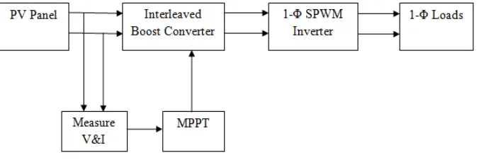
With the increase in the power demand and limited fossil fuels the renewable energy source plays a vital role to overcome these challenges. The fossil fuels based energy source causes environmental pollution. This led to the need for renewable energy sources (solar, wind, biomass) which is abundant and pollution free [1]-[3]. DC-DC converters play a vital role in photovoltaic (PV) systems as power interface. For stand-alone PV systems such as water pumps, LED, and signals, the MPPT technique is implemented [4]-[5]. Interleaved DC-DC converter is a technique where it can be implemented by paralleling the converters such that it reduces the switching stress and peak inductor current compared to conventional boost converter [6]. The block diagram of proposed system is as shown in fig.1.
Figure 1: Block diagram of proposed system
II. INTERLEAVED BOOST CONVERTER
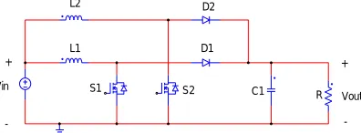
This paper proposes an interleaved boost converter. Interleaving is a technique which is implemented by paralleling the converters as shown in fig.2. By using this technique, the input current divides in the inductors which improves the reliability and makes the system to be efficient.
Vin S1 S2
D1 D2
L1 L2
C1 R
Vout
+ +
-
-Figure 2: Circuit configuration of Interleaved Boost converter
The interleaved boost converter consists of two stage parallel connected switches S1, S2; diodes D1, D2; inductors L1, L2 ;
capacitor C and load resistor R with common input source (Vin). The gating pulses to the interleaved boost converter is
given by , where n is the number of parallel stages. Here the two-phase interleaved boost converter is used hence
the phase difference is . [7]
The analysis of proposed converter is as follows:
Vin – Input voltage; V0 – Output voltage; L1 , L2 – Inductors; C1 – Capacitor; R – Load resistance;
Ts - Switching period; Fs= – Switching frequency; D- Duty cycle;
VL1 – Voltage across inductor L1; VL2 – Voltage across inductor L2;
iL1 – Change in the inductor current L1; iL2 – Change in the inductor current L2.
There are two modes of operation: Mode 1: (S1 – Closed, S2 – Opened)
In this mode the switch S1 is closed and switch S2 is opened, the equivalent circuit is as shown in fig 3.
Figure 3: Circuit configuration when switch S1 is closed
In mode 1, diode D1 is reverse biased while diode D2 is forward biased. The input supply energy to the inductor L1 and
the voltage across inductor L1 is given by:
= (1)
(2)
From the above equation, it can be concluded that the current in the inductor L1 increases linearly.
The voltage across inductor L2 is given by:
(4)
Since Vo is greater than Vin, From the above equation it can be concluded that current in the inductor L2 decreases
linearly.
Mode 2: (S1 – Opened, S2 – Closed)
In this mode the switch S2 is closed and switch S1 is opened, the equivalent circuit is as shown in fig 4.
Figure 4: Circuit configuration when switch S2 is closed
In mode 2, diode D1 is forward biased while diode D2 is reversed biased. Inductor L1 discharging and supplying energy
to the load resulting in fall of the inductor current iL1.
The voltage across inductor L1 is given by:
= (5)
(6)
Since Vo is greater than Vin, From the above equation it can be concluded that current in the inductor L1 decreases
linearly.
The voltage across inductor L2 is given by:
= (7)
(8)
From the above equation, it can be concluded that the current in the inductor L2 increases linearly.
The net change in the inductor current is zero
(9)
Substituting equation (2) and (6) in equation (9)
(10)
By solving the above equation, we get
(11)
The minimum inductor values L1 and L2 to operate converter in continuous conduction mode (CCM) are given by:
(12)
The capacitor Cis given by:
(13)
III.
MAXIMUM POWER POINT TRACKING
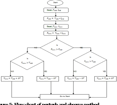
point tracking (MPPT) technique requires only some electronic circuits like voltage measurement and current measurement circuits to transfer the maximum power to the load. This technique overcomes the drawbacks of sun tracking system that is the usage of electric motors, gear box, and light sensors. The basic principle of MPPT technique involves that it uses an algorithm. The algorithm includes measurement of voltage and current then the calculation of power. Based on the different conditions of algorithm the duty cycle of power electronic switch of the DC-DC converter is adjusted to maintain the requirement of load. The P&O technique is used for MPPT.
Figure 5: Flow chart of perturb and observe method
The P&O algorithm is based on the calculation of the PV power and voltage by sampling the PV current and voltage. The flow chart is as shown in fig 5. In this approach, the module voltage is periodically given a perturbation and the corresponding output power is compared with that at the previous perturbing cycle. [8].
IV. SIMULATIONRESULTS
The interleaved boost converter and single phase inverter is designed and simulated for solar applications.
Figure 6: Waveforms of Inductor currents of conventional (in blue) and Interleaved Boost converter (in red)
Figure 7: Waveforms of currents through switch for conventional and Interleaved Boost converter
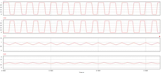
Fig.7 shows the current through switches for conventional and interleaved boost converter. Fig 8 shows switching states and change in the inductor currents of interleaved boost converter. Fig.9 shows the waveforms of open loop simulation with photovoltaic source, DC link voltage, and AC output. Fig.10 shows the waveforms of photovoltaic source, DC link voltage, and AC output with MPPT technique.
Figure 8: Switching states and Inductor currents of interleaved boost converter
The above fig.8 shows the switching states which are obtained from the P&O MPPT algorithm and it is given to MOSFET switches of interleaved boost converter and current trough inductors. The total input current is divided into two phases, resulting in reduction of the current rating of the switching devices.
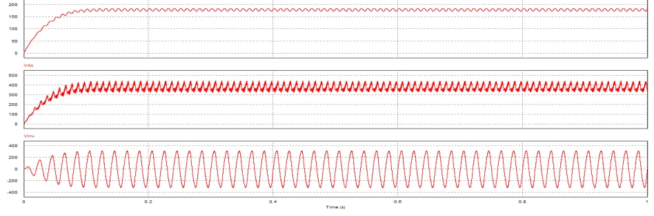
For simulation circuit, solar panels are connected in series and an output of 150VDC is obtained. This voltage is given to interleaved DC-DC boost converter as an input, it boost up the voltage from 150VDC to 300VDC by using interleaving technique. The output terminal of interleaved boost converter is connected to a single phase inverter therefore the DC output from the interleaved boost converter is inverted by single phase inverter. The Sinusoidal Pulse Width Modulation (SPWM) technique is used for pulse generation to MOSFET switches of the single-phase inverter. Finally at load side 240VAC, 50Hz supply is available.
Figure 10: Waveforms of PV array voltage, DC link voltage, Load voltage. (Closed loop)
V. CONCLUSION
In this paper the interleaved boost converter is designed and simulated for photovoltaic applications. The interleaved boost converter has advantages over traditional boost converters such as
1) It has less switching stress 2) Less peak inductor current
The proposed converter can also be used for fuel cell, ultra capacitors, and hybrid electric vehicle systems.
REFERENCES
[1] D.Meneses, F.Blaabjerg, O.Gracia, and J.Cobos, "Review and Comparison of Step-up Transformerless Topologies for Photovoltaic AC-Module Application", IEEE Transactions on Power Electronics, Vol.28, No.6, pp.2649-2663, June 2013.
[2] B. Alajmi, K.Ahmed, G.Philip, and B.Williams, "Single-Phase Single-Stage Transformerless Grid Connected PV System", IEEE Transactions on Power Electronics, Vol.28, No.6, pp.2665-267, June 2013.
[3] G. Velasco-Quesada, and F. Guinjoan-Gispert, R. Pique-Lopezand, M.Roman-Lumbrers, and A. Conesa-Rosa, “ Electrical PV Array Reconfiguration Strategy for Energy Extraction Improvement in Gridconnected PV Systems ” IEEE Trans. on Industrial Electronics, 2009. [4] S. Mekhilef, N. A. Rahim, and A. M. Omer, “A new solar energy conversion scheme implemented using grid-tied single phase
inverter”,Proceedings of IEEE TENCON-2000, Kuala Lumpur, Malaysia, 2000.
[5] Varin Vongmanee, “The photovoltaic pumping system using a variable speed single phase induction motor drive controlled by field oriented principle”, The 2004 IEEE Asia-Pacific Conference on Circuits and Systems, December 6-9, 2004.
[6] A.Thiyagarajan, S.G Praveen Kumar, A.Nandini , “Analysis and Comparison of Conventional and Interleaved DC/DC boost converter”, 2nd International Conference on Current Trends in Engineering and Technology, ICCTET’14.
[7] Power electronics, by Daniel W. Hart, TATA McGRAW-HILL EDITION.