International Journal of Research (IJR)
e-ISSN: 2348-6848, p- ISSN: 2348-795X Volume 2, Issue 10, October 2015Available at http://internationaljournalofresearch.org
Constraint Random Verification of Network Router for System
on Chip Applications Using Advanced Verification
Methodologies
1
Mrs .G.Shanmu gapriya
2
Janagama Raju
3
Mrs.P Sireesha
1
M.E. Associate Professor (ECE) CMRIT 2
M.Tech (VLSI) CMRIT 3
Assistant Professor (ECE) CMRIT Abstract:
The focus of this Paper is the actual implementation of Network Router and verifies the functionality of the five port router for network on chip using the latest verification methodologies, Hardware Verification Languages(s) and EDA tools and qualifies the Design for Synthesis and implementation. This Router design contains Four output ports and one input port, it is packet based Protocol. This Design consists of Registers, FSM and FIFO’s. The Verification goes on it finds functional coverage of the Network Router by using Verilog
Keywords: System Verilog; Fictional Coverage;
assertions; Randomization; FIFO; FSM;
Network-On-Chip; Verification Methodologies; Register blocks
I Introduction
90% of ASIC re-spins are due to Functional bugs. As the functional verification decides the quality of the silicon, we spend 60% of the design cycle time only for the verification/simulation. In order to avoid the delay and meet the TTM, we use the latest
verification methodologies and technologies and accelerate the verification process. This project helps one to understand the complete functional verification process of complex ASICs and SOC’s and it gives opportunity to try the latest
verification methodologies, programming
concepts like Object Oriented Programming of Hardware Verification Languages and sophisticated EDA tools, for the high quality verification.
The challenge of the verifying a large design is growing exponentially. There is a need to define new methods that makes functional verification easy. Several strategies in the recent years have been proposed to achieve good functional verification with less effort. Recent advancement towards this goal is methodologies. The methodology defines a skeleton over which one can add flesh and skin to their requirements to achieve functional verification. OVM (open verification methodology) is one such efficient methodology and best thing about it is, it is free. This OVM is built on System Verilog and used
effectively to achieve maintainability,
International Journal of Research (IJR)
e-ISSN: 2348-6848, p- ISSN: 2348-795X Volume 2, Issue 10, October 2015Available at http://internationaljournalofresearch.org
verifying Router Protocol by using system Verilog and OVM
II. Router Design Principles
Given the strict contest deadline and the short implementation window we adopted a set of design principles to spend the available time as efficiently as possible. This document
provides specifications for the Router is a packet
based protocol. Router drives the incoming packet which comes from the input port to output ports based on the address contained in the packet. The router is a” Network Router” has
a one input port from which the packet enters. It has four output ports where the packet is driven out. Packet contains 3 parts. They are Header, data and frame check sequence. Packet width is 8 bits and the length of the packet can be between 1 byte to 63 bytes. Packet header contains three fields DA and length. Destination address (DA) of the packet is of 8 bits.
The switch drives the packet to respective ports based on this destination address of the packets. Each output port has 8- bit unique port address. If the destination address of the packet matches the port address, then switch drives the packet to the output port, Length of the data is of 8 bits and from 0 to 63. Length is measured in terms of bytes. Data should be in terms of bytes and can take anything. Frame check sequence contains the security check of the packet. It is calculated over the header and data. The communication on network on chip is carried out by means of router, so for implementing better NOC, the router should be efficiently design.
This router supports four parallel
connections at the same time. It uses store and forward type of flow control and FSM
Controller deterministic routing which
improves the performance of router. The switching mechanism used here is packet switching which is generally used on network on chip. In packet switching the data the data
transfers in the form of packets between co-operating routers and Independent routing decision is taken. The store and forward flow mechanism is best because it does not reserve channels and thus does not lead to idle physical channels. The arbiter is of rotating priority scheme so that every channel once get chance to transfer its data. In this router both input and output buffering is used so that congestion can be avoided at both sides.
Features
Variable length of transfer word up to 64
bytes.
HEADER is the first data transfer.
Rx and Tx on both rising or falling edge
of serial clock independently 4 receivers select lines
Fully static synchronous design with one
clock domain
Technology independent VERILOG
Fully synthesizable.
The clock signal is provided by the master to provide synchronization. The clock signal controls when data can change and when it is valid for reading. Since ROUTER is synchronous, it has a clock pulse along with the data. RS-232 and other asynchronous protocols do not use a clock pulse, but the data must be timed very accurately. Since ROUTER has a clock signal, the clock can vary without disrupting the data. The data rate will simply change along with the changes in the clock rate. ROUTER is more suited for data stream applications. Communication between IP’s.
International Journal of Research (IJR)
e-ISSN: 2348-6848, p- ISSN: 2348-795X Volume 2, Issue 10, October 2015Available at http://internationaljournalofresearch.org
III. Operation
The Five Port Router Design is done by using of the three blocks. The blocks are 8-Bit Register, Router Controller and output block. The router controller is design by using FSM design and the output block consists of four FIFO’s combined together. The FIFO’s store data packets and when you want to send data that time the data will read from the FIFO’s. In this router design has four outputs i.e. 8-Bit size and one 8-bit data port. It is used to drive the data into router. we are using the global clock, reset signals, error signal and suspended data signals are the output’s of the router. The FSM
controller gives the error and
SUSPENDED_DATA_IN signals.
These functions are discussed clearly in below FSM description. The ROUTER can operate with a single master device and with one or more slave devices. If a single slave device is used, the RE (read enable) pin may be fixed to logic low if the slave permits it. Some slaves
require the falling edge (HIGH→LOW
transition) of the slave select to initiate an action such as the mobile operators, which starts conversion on said transition. With multiple slave devices, an independent RE signal is required from the master for each slave device.
Figure2: Internal Structure of Protocol
IV. Verification Methodologies
What is verification?
Verification is not a test bench, nor is it a series of testbenches. Verification is a process used to demonstrate that the intent of a design is preserved in its implementation. In this chapter, I introduce the basic concepts of verification, from its importance and cost, to making sure you are verifying that you are implementing what you want. The differences are presented between various verification approaches as well as the difference between testing and verification. It is also showed that how verification is key to design reuse, and challenges of verification reuse.
Importance of verification
Today, in the era of multi-million gate ASICs and FPGAs, reusable intellectual property (IP), and system-on-a-chip (SoC) designs, verification consumes about 70% of the design effort. Design teams, properly staffed to address the verification challenge, include engineers dedicated to verification. The number of verification engineers can be up to twice the number of RTL designers.
Functional coverage
Functional coverage is another
International Journal of Research (IJR)
e-ISSN: 2348-6848, p- ISSN: 2348-795X Volume 2, Issue 10, October 2015Available at http://internationaljournalofresearch.org
V. Test Bench Architecture
A collection of all test specifications for a given area. The Test Plan contains a high-level overview of what is tested and what is tested by others for the given feature area. The test plan is implemented using OVM test component. Generally the method to write a test case is to define a base test in which all the environment is instantiated and all the common configurations used for all the test cases are written
Test Cases:
Control Test Case
Control test case is mainly targeted for the Master section of the Router. Its purpose is to check whether the device is responding to the standard request or not and to check the control endpoints of the device. It generates random standard requests to the Router devices and look for the response for the device. It also checks the operation of the endpoint 0 controller in the
device. It uses the sequences like
set_address_command,set_confioguration_comm
and, get_confi- guration_command,
get_status_command, set_feature command.
Data Receive Test Case
This test case is used to verify the functionality of the master receiver of the Router device. This test case first configures the device for use by using standard requests, issues the command to receive the data from the external i2c device and finally retrives the data from the master reciever FIFO by using data read commands. It uses standard sequences, write register sequence, data read sequence from the sequence library.
Slave Data Transmit Test Case
This test case is to verify the slave transmitter of the Router section, but any way this test case should make sure some data in slave transmit FIFO. So the test case will first calls standard commands to set the device up , then it has to write some data on the slave
transmit FIFO and finally slave is ready to transmit the data. The transmission happens when external master initiates the transfer. It uses standard sequences, data write sequences, register write sequences from the sequence library.
Slave Data Receive Test Case
This test case is used to verify the functionality of the slave receiver of the Router device. This test case first configures the device for use by using standard requests, slave receives the data from the external i2c device and stores it in the slave receiver FIFO .Then agent reads the FIFO by using data reads commands. It uses standard sequences, write register sequence, data read sequence from the sequence library.
VI Results &Coverage Reports
Code Coverage
The tests are written according the test plan and the tests are made into a single regression which contains all the tests and a Perl script is written to run all the tests. This script can also run with the coverage option to see the coverage results. It creates a html page which contains the results of the tests that are run in that regression. When this script is run with the coverage option, it creates a directory with name “report” and dumps all the coverage html reports generated by the Questa tool. The extent of verification cannot be judged manually. T
he Questa tool offers coverage aspects on the written RTL code. Code coverage measures the amount of HDL code that has been exercised by all the tests. It not only checks the coverage in terms of lines covered, but the states covered in state machines, the values of the signals that are toggled etc. By running the tests in the testplan the coverage that is attained is as follows
International Journal of Research (IJR)
e-ISSN: 2348-6848, p- ISSN: 2348-795X Volume 2, Issue 10, October 2015Available at http://internationaljournalofresearch.org
due to some part of the code which is kept for some invalid signalling. This percentage of the missed coverage is due to the conditions that has different possibilities like a condition ((x==1) or (y==1)). Tool creates the possible combinations of the condition as 00,01,10,11. Attaining all the conditions is cumbersome to achieve. Another reason is that the invalid FSM transitions that are picked up by the tool. The tool extracts the state machine from the HDL code. In that process some invalid transitions are created that are not present in the state machine which is designed. We can also eliminate the transitions from the coverage and get the coverage 100%.
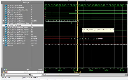
Simulation Results
The below figures shows the simulation results of test cases applied to the DUT . figure 6.shows the response of the FSM block of Router, here we give the Directed Test sequences at the same time Random also. Figure 6.shows the master transmitter sending random data to the external slave device.
Figure 6: FSM Simulation Results
The below figures shows the simulation results of test cases applied to the DUT . figure 7.shows the response of the Design Under Test using different test vectors, here we give the Directed Test sequences at the same time Random also. This DUT response explain below.
Figure 7: Simulation Results of Router Protocol-
Data_in[1:7] = input =deferent data packets
Data_in[0] = 11111001
Output : Ch_out1 = 8’bXXXXXXXX
Ch_out2 = data_in,
Ch_out3 = 8’bXXXXXXXX.
Ch_out4 = 8’bXXXXXXXX.
After 80ns again applying inputs immediately
output obtained, because of no delay elements.
Data_in[1:7] = input =deferent data packets
Data_in[0] = 11111000
Output : Ch_out2 = 8’bXXXXXXXX,
Ch_out1 = data_in,
Ch_out3 = 8’bXXXXXXXX
Ch_out4 = 8’bXXXXXXXX.
V Applications
International Journal of Research (IJR)
e-ISSN: 2348-6848, p- ISSN: 2348-795X Volume 2, Issue 10, October 2015Available at http://internationaljournalofresearch.org
protocol standards..
VII Conclusion
As the functional verification decides the quality of the silicon, we spend 60% of the
design cycle time only for the
verification/simulation. In order to avoid the delay and meet the TTM, we use the latest verification methodologies and technologies and accelerate the verification process. This project helps one to understand the complete functional verification process of complex ASICs an SoC’s and it gives opportunity to try the latest
verification methodologies, programming
concepts like Object Oriented Programming of
Hardware Verification Languages and
sophisticated EDA tools, for the high quality verification.
In this project I have verified the functionality of the ROUTER with the latest Verification methodology i.e. System Verilog and observed the code coverage and functional coverage of ROUTER by using cover points and different test cases (like constrained, weighted and directed test cases). By using these test cases I had improved the functional coverage of the ROUTER. In previous we using Verilog for verify the functionality here we can’t find that results are correct or not by using verification methodologies we get 100% functional coverage. In this project I used one master and four slaves to monitor the ROUTER. Thus the functional coverage of the ROUTER was improved.
The results shows that System Verilog methodology can be used to make reusable test
benches successfully. Large part of the test bench is made reusable over multiple projects. even though this reusability is limited to the interfaces. A large class of devices that are build on these interfaces can be verified successfully. Once these components are made the amount of time required to build test benches for other projects can be reduced a lot.
References
[1] D.Chiou,“MEMOCODE2011Hardware/S
oftwareCoDesignContest”,https://ramp.ec e.utexas.edu/redmine/Attachments/esign Contest.pdf
[2] Xilinx,“ML605HardwareUserGude”,http:
//www.xilinx.com/support/documentation /boardsand its/ug534.pdf
[3] Xilinx,“LogiCOREIPProcessor Local
Bus (PLB) v4.6”,
http://www.xilinx.com/support/document ation/ip ocumentation/plb v46.pdf
[4] “Application Note: Using the Router
Interface to Communicate Motorola, ANN91/D Rev. 1, 01/2001. Cisco Router OSPF: Design& Implementation Guide, Publisher: McGraw-Hill
[5] “LRM”, IEEE Standard Hardware
Description Language Based on the Verilog Hardware Description Language