Method of Additive Regularization of Field Integrals in the Problem
of Electromagnetic Diffraction by a Slot in a Conducting Screen,
Placed before a Dielectric Layer
Vladimir M. Serdyuk*
Abstract—We present a rigorous solution of a two-dimensional problem of stationary electromagnetic plane wave diffraction by a slot in a perfectly conducting screen having finite thickness in the presence of a plane dielectric layer behind the screen. For obtaining this solution, the method of additive regularization of singularities for field diffraction integrals is developed. This method is suitable for the cases of transparent, absorbing and amplifying dielectric. It reduces to explicit extraction of singularities in the form of supplementary singular integral terms, which describe waveguide modes of a dielectric layer. On the bases of the obtained solution, the conditions of optimum diffraction excitation for such modes are investigated in dependence of geometrical parameters of the problem for the cases, when these parameters are of the order of the radiation wavelength.
1. INTRODUCTION
The problem of plane wave diffraction by a slot in a perfectly conducting screen is one of the primary model problems of the electromagnetic waves propagation theory [1, 2], because a slot can be considered as the simplest model of an aperture. That is why during a lot of years many authors have solved this problem using various methods (see, for example, [3–10]). A rigorous approach to solving such problems is provided by the eigen-modes technique [11], which is successfully applied to simulation of fields in diffraction, waveguide, and resonator structures of various geometries (see, for example, [12–15]). The rigorous approach, based on the well-known eigen-modes technique [11] provides the opportunity to obtain a rigorous solution for electromagnetic diffraction by a slot in an infinitesimally thin conducting screen [16]. For slots in screens of finite thickness, direct utilization of the eigen-modes technique gives a stable solution only in the cases of thick conducting screens with the thickness of the order of several wavelength and more [13], because for thin screens, the main system of equations becomes ill-conditioned. But if one applies known methods of regularization of linear systems to such a system, for example, the Tichonov’s regularization method [17], then the resulting solution of slot diffraction problem becomes suitable for conducting screens of finite thickness [18], including the values much less than the radiation wavelength.
It should be noted that the majority of works on this topic consider the slot structures without dielectrics, and the structures, having the simple inclusions of the type of plane-layered dielectrics, are rather seldom studied using the eigen-modes technique, because for them the procedure of field integrals computation becomes complicated. In [19], the presence of a dielectric behind the screen with a slot has been taken into account, but the authors consider semi-infinite strongly absorbing dielectric medium. In the presence of plane-layered dielectrics, the integrands of field integrals show appearance of multipliers, which display the processes of reflection and refraction on dielectric interfaces. They
Received 29 October 2018, Accepted 3 January 2019, Scheduled 2 March 2019
* Corresponding author: Vladimir M. Serdyuk ([email protected]).
can tend to infinity at some values of propagation parameter of spectral plane waves, which serves as the argument of integration. Such values of the propagation parameter determine waveguide modes of dielectric layered structures, which can propagate on infinitely great distance along the boundaries of a layer. For example, even for a homogeneous plane dielectric layer, the coefficients of reflection and refraction [20, 21] contain a denominator, which vanishes at some values of the propagation parameter, corresponding to waveguide modes of this layer [22].
As a result, field integrals acquire poles, which essentially complicates the procedure of their computation and determining the fields in various points of space, because the usual methods of numerical computation of integrals (see, for example, [23]) presuppose boundedness of integrands and their derivatives. Application of purely numerical methods to such problems, namely the methods of finite differences or finite elements [24, 25], also entails specific severities [26, 27], because these methods require specification of conditions for fields on great distances from an obstacle (i.e., at infinity), but here, besides an incident wave, the amplitudes of waveguide modes can appreciably differ from zero, and they are unknown values to be determined by solution of diffraction problem [28].
General recommendations on calculation of singular integrals are known [29, 30]. They are reduced to the method, which can be called as additive regularization and suppose explicit extraction of singularity in the form of separate summand. It is written as an integral of an additional function, which behaves about a pole as an initial singular integrand. The same function, but with the opposite sign, is added to the last in the order of compensation of its singularity. The idea is simple, but as far as we know, it has not been applied to the problems of diffraction by a slot and dielectric layers up to now. Only in [31] this idea has been realized in application to the problem of diffraction by a thin conducting strip with a near-located transparent dielectric layer. In the present work, we shall consider solution of the diffraction problem for a slot structure with a plane dielectric layer, using the eigen-mode technique and shall suggest the procedure of additive regularization, elaborated for the cases of transparent and absorbing layer. From the practical point of view, the last case is of interest in connection with multiplicity of applications of electromagnetic conversion slot systems in physics, engineering, biology, and medicine (see, for example, [22, 32–36]), when one cannot neglect dielectric absorption or the presence of amplification (negative absorption). In the given work, we consider the case of diffraction by one slot in a screen with a homogeneous dielectric behind that, but the method, used in our work, can be effectively applied to the cases when one considers a multilayered dielectric instead of homogeneous one, and to the cases when diffraction occurs due to presence of strip, or a screen with periodical system of many slots or strips, instead of a screen with one slot, as in our work.
2. GENERAL SOLUTION OF DIFFRACTION PROBLEM
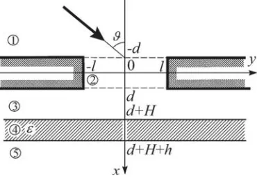
Let us consider 2D stationary problem of plane wave diffraction by a slot in a perfectly conducting screen of finite thickness, placed parallel to a plane dielectric layer at some distanceH(Fig. 1). Let the plane of diffracting wave incidence coincide with the coordinate xy plane, which is orthogonal to the z axis, parallel to the infinite slot edges (Fig. 1). In this case, the Maxwell equations admit separation of the field into two polarizations H and E (in optics, they are specified as TE and TM [20]), which are determined by an independent complex scalar function u(x, y) of two coordinates x and y. It should satisfy the scalar Helmholtz equation [1, 11, 20]
∂2u ∂x2 +
∂2u ∂y2 +k
2ε(x)u= 0 (1)
wherek=ω/cis the wavenumber;ωis the circular frequency of field;cis the light speed in vacuum,ε(x) is the piecewise constant function, equals unity in empty space and the constant dielectric permittivity of a layer εin it, i.e., ε(x) = εat d+H ≤x ≤d+H+h and ε(x) = 1 in air (in vacuum). At that, in the Gaussian system of units, the spatial components of the electric and magnetic vectors for every polarization are expressed in terms of the scalar field function u in the following way [1, 11, 20]
Ez
ε−1(x)Hz
=u
Hx
−Ex
=−i
k ∂u ∂y
−Hy
Ey
=−i
k ∂u
∂x (2)
various values are present for different polarizations, because the values of independent field functions in the same points of space for these polarizations differ from each other owing to discrepancy of boundary conditions. Nevertheless, such a form of writing for the fields is entirely true, because for the H polarization the componentsHz,Ex andEy, written in the lower lines of (2), identically vanish, and
for theE polarization, in turn the componentsEz,Hxand Hy, presented in the upper lines, equal zero.
In these equations and anywhere below, the exponential factor exp(−iωt), determining the temporal dependence of fields, is omitted.
Figure 1. Geometry of the problem of the plane wave diffraction by a slot in a thick conducting screen and by a parallel plane dielectric layer: the relative positions of objects and the resolving regions of field propagation.
The boundary conditions for these fields are reduced to the known requirements of continuity for tangential components of electric and magnetic fields on the dielectric interfaces and of vanishing for tangential electric components on perfectly conducting surfaces [1, 11, 20]. According to Eq. (2), these requirements can be formulated in the form of the following conditions for the field function u and its normal derivative ∂u/∂xor∂u/∂y
(u)x=d+H−0 = εν(u)x=d+H+0 εν(u)x=d+H+h−0 = (u)x=d+H+h+0 (3a)
(∂u/∂x)x=d+H−0 = (∂u/∂x)x=d+H+0 (∂u/∂x)x=d+H+h−0 = (∂u/∂x)x=d+H+h+0 (3b)
where ν equals zero for the H polarization, ν = 1 for the E polarization, and the symbol “0” denotes an infinitesimal positive value,
(1−ν)(u)x=∓d+ν(∂u/∂x)x=∓d= 0 for |y|> l (4a)
(1−ν)(u)y=∓l+ν(∂u/∂y)y=∓l= 0 for |x|< d (4b)
i.e., either the function u or its normal derivative (∂u/∂x or ∂u/∂y) should vanish on conducting boundaries of a screen for theH or E polarization.
Let us separate all space of field propagation on 5 regions of simple geometry, denoted by the numbers in Fig. 1, whose boundaries are straight lines or straight-line segments, parallel to the coordinate axes. According to ideology of the eigen-modes technique [11], in every such region, we can represent the field functionuas a superposition of plane waves, which are solutions of the Helmholtz Equation (1), taking into account possible restrictions on field propagation along they axis.
Let the incident plane wave be
u0(x, y) =α−ν0 exp{ik[α0(x+d) +β0y]} (5)
whereα0 = cosϑandβ0 = sinϑare the parameters of wave propagation in thexandyaxes (α20+β02 = 1),
and ϑ is the angle of wave incidence on the surface of a screen. Our choice of the coefficient in the right-hand side of Eq. (5) before the exponent provides unit value for amplitude of thezorycomponent of the electric vector in the cases of theH and E polarization, respectively.
Then, in region 1 before the screen (atx≤ −d) one can write the following representation for the field
u1(x, y) = α−ν0 {exp[ikα0(x+d)]−(−1)νexp[−ikα0(x+d)]}exp(ikβ0y)
+(−1)ν +∞
−∞ α
where the incident wave and the wave reflected from a screen are separated explicitly, and the diffraction field is presented in the form of an integral over plane waves. This integral is nothing but an expansion of the field on the plane x = −d in a Fourier integral, whose every plane-wave component has the additional multiplier exp[−ikα(x+d)]. It describes propagation of this component outside the given plane and provides validity of the Helmholtz Equation (1), if we set
α=1−β2 (7)
For the field (6) not to increase at large negative x, it is necessary to choose the brunch of the square root in Eq. (7) with nonnegative imaginary part.
In region 2 (at−d≤x≤d,−l≤y≤l), a spectrum of eigen waves inside a slot should be discrete, because this region is bounded in they axis by perfectly conducting surfaces
u2(x, y) = +∞
n=1
α−ν(s)na(s)nexp(ikα(s)n(d+x)) + (−1)νb(s)nexp(ikα(s)n(d−x)) cos(kξ(s)ny)
+iα−ν(a)na(a)nexp(ikα(a)n(d+x)) + (−1)νb(a)nexp(ikα(a)n(d−x)) sin(kξ(a)ny)
(8)
where the propagation parameters of symmetrical (index s) and antisymmetrical (index a) modes on the given axis are determined by the following
ξ(s)n= π
kl
n−1 +ν 2
; ξ(a)n= klπ
n−ν
2
; α(s,a)n =
1−ξ(s2,a)n (9)
The first two equations of Eq. (9) provide validity of the boundary conditions in Eq. (4b) for slot modes, and the last one guarantees validity of the Helmholtz Equation (1) for those.
In region 3, between the screen and a dielectric layer (atd≤x≤d+H), one should consider again a continuous spectrum of eigen waves
u3(x, y) =
+∞
−∞
α−ν
D(β)A(β){Δ(β) exp[ikα(x−d)] +R(β) exp[ikα(2H+d−x)]}exp(ikβy)dβ (10) And in the remaining two regions, we should take into account continuous characteristic of the spectrum. In region 4 (inside the dielectric, at d+H ≤x≤d+H+h)
u4(x, y) =
+∞
−∞
α−νT34(β)
D(β) A(β){exp[ikγ(x−H−d)]
+R43(β) exp[ikγ(2h+H+d−x)]}exp[ik(αH+βy)]dβ (11)
where the parameter of normal propagation for waves in a dielectric is
γ =ε−β2 (12)
and in region 5 (behind the dielectric, at x≥d+H+h)
u5(x, y) =
+∞
−∞
α−νT34(β)T45(β)
D(β) A(β) exp{ik[α(x−h−d) +γh+βy]}dβ (13) In expressions (6), (8), (10), (11), (13), the valuesB(β),A(β) anda(s,a)n,b(s,a)nrepresent unknown mode
amplitudes in various regions, to be determined from equations of field joint on the boundaries between these regions. Additional amplitude coefficients under the integration and sum signs are separated specially to satisfy various additional conditions, which appear in the following consideration. For example, the multipliers Δ(β), R(β), T34(β), etc. provide validity of the boundary conditions (3) on
two plane boundaries of a dielectric layer. If
R43(β) = γ−αε ν
γ+αεν; T34(β) =
2α
γ+αεν; T45(β) =
2γεν
γ +αεν; R(β) =R43(β)
e2ikγh−1
(14a)
Δ(β) = 1−R243(β) exp(2ikγh) (14b)
D(β) = Δ(β) + (−1)νR(β)e2ikαH = 1−R432 (β)e2ikγh+ (−1)νR43(β)
e2ikγh−1
then the continuity conditions for tangential components of electric and magnetic fields on the dielectric interfaces in Eq. (3) are valid identically for every mode of continuous spectrum, i.e., for every plane wave component of integrals in Eqs. (10), (11) and (13). Such wave components in various regions of the half-space behind the screen, coupled by boundary conditions on the interfaces x=H and x=H+h, form a united eigen-mode of this half-space.
Here, the values Rij(β) and Tij(β) in Eq. (14a) have the meaning of amplitude coefficients of
reflection and refraction for a plane electromagnetic wave with the tangential propagation parameter β on the plane boundary between dielectric media with the numbers i and j (j =i+ 1 or j =i−1; for definiteness, we assume that a wave incidents from the medium i) [20, 21]. At that, the ratio of the values R(β) and Δ(β) in Eq. (14) has the meaning of the coefficient of reflection for the layer as a whole.
Hence, the fields in various regions, presented by the integrals and discrete expansions in Eqs. (6), (8), (10), (11), (13), satisfy all necessary boundary conditions, except for the conditions in Eq. (4a) on conducting surface of a screen. To those one must add the continuity conditions for tangential components of electric and magnetic fields on the upper (−l < y < l; x=−d) and lower (−l < y < l; x=d) boundaries of a slot (see Fig. 1), because there is no any barrier for propagation of field
(u)x=∓d−0 = (u)x=∓d+0
(∂u/∂x)x=∓d−0 = (∂u/∂x)x=∓d+0
for |y|< l (16)
Substitution of expressions (6), (8), (10) for the fields into the boundary conditions in Eqs. (4a) and (16) yields integral equations, determining mode amplitudes in various regions. These equations are sufficiently cumbersome, but they can be simplified in several steps. At first, one should separate symmetrical and antisymmetrical parts of the integral amplitudesA(β) and B(β) on the parameter of integration β
A(β) =A(s)(β) +A(a)(β); A(s)(−β) =A(s)(β); A(a)(−β) =−A(a)(β)
which leads to separation of a Fourier integral into the sum of symmetrical and antisymmetrical parts on the coordinate argument y
+∞
−∞ A(β)e
ikβydβ = 2
+∞
0
A(s)(β) cos(kβy)dβ+ 2i +∞
0
A(a)(β) sin(kβy)dβ
(similarly, the separation is performed for the amplitude B(β)). The parameters of normal mode propagation α in Eq. (7) and γ in Eq. (12) outside and inside the dielectric, and also all values, determined by these parameters, do not depend on the argument of integration β itself, but are determined only in terms of its square, i.e., they are symmetric on the given argument. This provides separation of all equations into symmetrical and antisymmetrical parts. Furthermore, one can transform the form of equations from coordinate representation on the argumenty to spatial frequency representation. For this purpose, every equation should be multiplied on cos(kβy) and sin(kβy), or on cos(kξ(s)ny) and sin(kξ(a)ny), respectively, dependent on its coordinate symmetry, and then it should be
integrated over ally. At that, we should take into consideration the orthogonality conditions for modes of continuous and discrete spectra on they axis
+∞
−∞ cos(kβy) cos(k
¯ βy)dy =
+∞
−∞ sin(kβy) sin(k
¯
βy)dy= π kδ
β−β¯ +l
−l cos(kξ(s)ny) cos(kξ(s)my)dy =lδnm(1 +δn1);
+l
−l sin(kξ(a)ny) sin(kξ(a)my)dy =lδnm
whereδ(β) is the Dirac delta function [20], andδmn are the Kroneker symbols (δmn= 1 at m=nand
δmn = 0 atm=n). As a result, we obtain
B(s,a)(β) = kl 2π
+∞
n=1
a(s,a)n+b(s,a)nexp(2ikα(s,a)nd) Q(sn,a)(β) (17a)
A(s,a)(β) = kl 2π
+∞
n=1
α10−2νQ(sn,a)(β0)−
+∞
0
α1−2νB(s,a)(β)Q(sn,a)(β)dβ
= 1 2α
1−2ν (s,a)n
a(s,a)n−b(s,a)nexp(2ikα(s,a)nd) (1 + Θνδ1n) (17c)
+∞
0
α1−2νΨ(β)A(s,a)(β)Q(sn,a)(β)dβ
= 1 2α
1−2ν (s,a)n
a(s,a)nexp(2ikα(s,a)nd)−b(s,a)nexp(2ikα(s,a)nd) (1 + Θνδ1n) (17d)
where Θ = 1 for symmetrical modes and Θ = 0 for antisymmetrical modes,
Q(sn,a)(β) = 2 l
l
0
cos(kξ(s)n) cos(kβy)
sin(kξ(a)n) sin(kβy)
dy =
2βvξ(s1−v,a)n β+ξ(s,a)n
·sin[kl(β−ξ(s,a)n)]
kl(β−ξ(s,a)n)
(18)
are the overlap integrals for various regions,
Ψ(β) = Δ(β)−(−1)νR(β) exp(2ikαH)
The relationships of Eqs. (17a) and (17b) express the amplitudes of continuous spectrum modes outside the slot in terms of amplitudes of discrete spectrum modes inside that. Substitution of these relationships into Eqs. (17c) and (17d) provides the opportunity to exclude amplitudes of continuous spectrum modes from the boundary equations. For new amplitude values
c±(s,a)n=a(s,a)n±b(s,a)n
/2 (19)
the system of linear algebraic equations in slot modes takes the form
+∞
m=1
c+(s,a)mL+(s,a)mn+c−(s,a)mL−(s,a)mn
= 2α10−2νQn(s,a)(β0) (20a) +∞
m=1
c+(s,a)mM(s+,a)mn+c−(s,a)mM(s−,a)mn
= 0 (20b)
where the matrices of coefficients are written as follows
L±(s,a)mn = Vmn(s,a)ζ(s±,a)m+α(s1−,a)2νnζ(s∓,a)n(1 + Θνδ1n)δmn (21a)
M(s±,a)mn = ±V˜mn(s,a)ζ(s±,a)m±α(1s,a−2)νnζ(s∓,a)n(1 + Θνδ1n)δmn (21b)
ζ(s±,a)n = 1±exp(2ikα(s,a)nd) (21c)
Vmn(s,a)= kl π
+∞
0 α
1−2νQ(s,a)
m (β)Q(sn,a)(β)dβ
˜
Vmn(s,a)= kl π
+∞
0
Ψ(β) D(β)α
1−2νQ(s,a)
m (β)Q(sn,a)(β)dβ
(22)
and the required amplitudes of discrete spectrum modes are expressed in terms of new amplitudes in Eq. (19) by the formulas
a(s,a)n=c+(s,a)n+c−(s,a)n b(s,a)n=c +
(s,a)n−c−(s,a)n (23)
on the argument of integration β, the corresponding equations can be written uniformly for all three regions of continuous field spectrum behind the screen
Ez
ε−1(x)Hz
=
+∞
0
f+ m(β, x)
D(β) F
+(
β, y)dβ Hx −Ex = +∞ 0
fm−(β, x) D(β) F
+(
β, y)dβ (24a) −Hy Ey = +∞ 0
fm+(β, x) D(β) F
−(β, y)βdβ (24b)
wherem is the index (number) of the region of field propagation (m= 3; 4; 5),
F±(β, y) = A(β) exp(ikβy)±A(−β) exp(−ikβy) (25a)
A(±β) = A(s)(β)±A(a)(β) (25b)
f3±(β, x) = αM−ν
1−R432 (β)e2ikγh
eikα(x−d)±R43(β)
e2ikγh−1
eikα(2H+d−x)
(26a)
f4±(β, x) = α−νγMT34(β)
eikγ(x−H−d)±R43(β)eikγ(2h+H+d−x)
eikαH (26b)
f5±(β, x) = αM−νT34(β)T45(β)eikα(x−h−d)eikγh (26c)
M = (1∓1)/2, i.e.,M = 0 for the upper index “plus” andM = 1 for the upper index “minus”. A similar compact notation can be used for the fields before the screen in Eq. (6)
Ez
Hz
= G+0(x) exp(ikβ0y) +
+∞
0 f +
1 (β, x)G+(β, y)dβ (27a)
Hx
−Ex
= G−0(x) exp(ikβ0y) +
+∞
0
f1−(β, x)G +(
β, y)dβ (27b)
−Hy
Ey
= G+0(x) exp(ikβ0y) +
+∞
0
f1+(β, x)G−(β, y)βdβ (27c)
where
G±0(x) = αM−ν0 {exp[ikα0(x+d)]∓(−1)νexp[−ikα0(x+d)]}
G±(β, y) = B(β) exp(ikβy)±B(−β) exp(−ikβy) B(±β) = B(s)(β)±B(a)(β)
f1±(β, x) = αM−νexp[−ikα(x+d)]
Note that the main system of Equation (20) of diffraction problem is infinite-dimensional, and it requires reduction of the given system to a system of finite dimensions [37]. For the problems of a similar type, such reduction is realized in the following manner. One takes the finite numberN of slot modes, and all integrals over modes of continuous spectrum are replaced with integral sums using quadrature formulas also with finite number of summands. After determining amplitudes in all regions, one computes the spatial field components in Eqs. (24), (27) on all boundaries of regions and estimates the error of validation of the conditions in Eqs. (3), (4a) and (16) on the both sides of each boundary. The error should be in the 7–8th decimal sign for plane boundaries of a dielectric layer and in the 3–4th decimal sign for the boundary of a screen with a slot. If the error magnitude does not exceed the pointed values, then reduction can be interpreted as satisfactory; otherwise, one should increase the number of modes under consideration inside and outside of a slot.
can be small. Then, at not great screen thickness 2d, the determinant of the matrix in Eq. (21) of the main system of Equations (20) also becomes small in magnitude. In order to overcome such impediment, one can apply the Tichonov’s method of regularization [17], whose use does not significantly complicate the solving procedure for the system in Eqs. (20), but allows for obtaining stable solutions of this system at arbitrary screen thickness (slit depth), including the cases, when this thickness is of order of magnitude of the wavelength and less. In our case, the regularization procedure for the system of equation is performed in the same way as in the case of a solitary slot without a dielectric [18].
3. REGULARIZATION OF FIELD INTEGRALS
Up to this point, we have not taken into account possible appearance of singularities in the integrals in Eqs. (22) and (24). Meanwhile, for some values of the argument of integration β =βj the common
denominator D(β) of Eq. (15) of their integrands can be very small in magnitude or at all reduces to zero
D(βj) = 1−R243(βj) exp(2ikγjh) + (−1)νR43(βj)[exp(2ikγjh)−1] exp(2ikαjH) = 0 (28)
where γj and αj are the values of parameters of normal propagation in a dielectric of Eq. (12) and in
air of Eq. (7), corresponding to the tangential propagation parameter βj. Consequently, in the points
β = βj the integrals in Eqs. (22) and (24) have singularities, which are characterized by sharp rise
of integrands up to infinity. Physically, such values of the propagation parameter correspond to the waveguide modes of a plane dielectric layer with the thicknessh, which is arranged parallel to a perfectly conducting screen without a slot at the distanceH(Fig. 1). Analysis shows that the zeros of the function D(βj) in Eq. (28) are of the first order, i.e., they are simple poles of the integral coefficients in Eq. (22)
(of the integral expressions for the fields (24)), whose number is finite. On the complex plane of β, they are located near the interval of the real axis from 1 to Re(ε1/2), and their displacement from this axis depends on the value of absorption in a dielectric. For transparent layer, waveguide modes have a real parameter of normal propagation in a dielectric γj of Eq. (12) and a purely imaginary parameter
outside it (in air)αj of Eq. (7)
αj =iτj; τj =−iαj =
βj2−1 (29)
where τj is the real parameter of exponential decay of a waveguide mode in air, because behind the
layer, its field in Eq. (26c) decays exponentially with the rise of the normal coordinate x. Before the layer, the field in Eq. (26a) decreases as the hyperbolic sine (for the H polarization) or cosine (for the E polarization) at moving away in the screen direction.
In the absence of absorption, when the dielectric permittivityεis a real value, all poles are located exactly on the real axis of β, on which integration is carried out in Eqs. (22) and (24). But under appearance and rise of absorption, poles shift more and more away from this axis, so that at great absorption the distances between poles and the contour of integration are sufficiently great, and the valueDin itself becomes not small in magnitude anywhere on the contour. In this case, one can neglect the presence of poles, which are far from the real β axis and perform calculation as in the case of the absence of a dielectric [18]. However, if the value of absorption is small, or it is absent at all, then the presence of poles near the real axis should be taken into consideration necessarily. Here, about poles, integrands very rapidly change under small changes of argument of integration, and consequently, usual methods of computation of integrals [23] for Eqs. (22) and (24) are inapplicable, even if the poles are not located exactly on the contour of integration.
In order to get around this difficulty, one can use the method of regularization of singular integrals [29, 30], which is reduced to the known technique of additive extraction of a singularity from their integrands. In [31], this method has been developed for transparent dielectrics, here it is extended to the cases of possible presence of absorption in a dielectric layer. As before, we shall construct the regularization procedure without outgo on the complex plane beyond the real axis of the argument β, in order to calculate regularized integrals afterwards using standard numerical methods without any complications. Therefore, in the general case of weakly absorbing dielectric, it is more convenient to search not zeroes of Equation (28) but minima of the square of the modulus for the left-hand side of this equation on the real axis of the given argument
Such minima represent projections of poles (zeroes of the functionD) from the complex plane of β on the real axis.
Let construct a simplified change for the function D(β) of Eq. (15), which adequately replicates its asymptotic behavior near a singular point and can be used instead of the functionDin regularizing additives. Let the given function have J simple zeroes near the real axis of the argument β, which determine poles of corresponding integrals with this function. Near every simple pole, or a pole of the 1st order (zero of the function D), on the real axis, the given function can be presented in the form of the first two terms of the Taylor series
D(β)∼Dj + (β−βj)Dj (31)
where βj is the minimum of the square of the modulus of the function D, numbered by the index j
(j = 1,2, . . . , J); Dj =D(βj) is the value of the function in this minimum; and the prime denotes its
derivative in the given point. It can be shown that the ratio of an analytic function and its derivative Dj/Dj in the point of modulus minimum is an imaginary value on the real axis (for complex ε) or
equals zero (for realε), and for the functionD, specified by Equation (15), this value is nonpositive at Imε≥0. Hence, it is useful to rewrite the decomposition of Eq. (31) in a more convenient form
D(β)∼iqj(β−βj−iSj) Sj =iDj/Dj (32)
where qj = −iDj is the derivative, multiplied by −i, Sj =Dj/qj. From here, one can determine the
change
1
D(β) → −
ip
qj[p(β−βj)−ipSj]
at β→βj (33)
where we have introduced the new dimensionless positive parameter p, whose meaning will be cleared below. Let introduce one more parameter σj, setting
pSj = tan(pσj)
From the last equation we give the definition of this parameter
σj =p−1arctan(pSj) (34)
and the new expression for approximate representation of the singular multiplier in Eq. (33) is
1
D(β) → −
ip
qj[p(β−βj)−itan(pσj)]
(35)
Now, the product p(β−βj) can be replaced with the hyperbolic sine sinh[p(β−βj)] of that and the
unit multiplier of the tan can be changed for the hyperbolic cosine of the same value cosh[p(β−βj)];
it is obvious that such a change does not somehow distort behavior of the denominator for the singular multiplier of Eq. (35) near the pointβ =βj. Then for this multiplier we have the following representation
D−1(β)→ −Γj−1χj(β) (36)
where
Γj = qj
1 +p2S2
j (37)
χj(β) = ip/sinh[p(β−βj −iσj)] (38)
The change of the presentation in Eq. (32) for Eq. (36) provides conservation of the asymptotic for constructed function near the pointβ =βj and rapid decrease of its magnitude to zero at moving away
from this point.
Additional regularizing components for singular integrals are constructed on the basis of the new singular function in Eq. (36). Then the procedure of additive regularization for the integral in Eq. (22) can be written in the following way
+∞
0
f(β) D(β)dβ=
+∞
0
⎛ ⎝f(β)
D(β) +
J
j=1
f(βj)χj(β)
Γj ⎞
⎠dβ−ipJ
j=1
f(βj)
Γj
+∞
0
dβ
sinh[p(β−βj−iσj)]
where summation is taken over all points of minima of the square of the modulus of the functionD in Eq. (15), and all regular functions of integrand are merged in one function f(β). One should take into account that all values ofβj are above the unity in magnitude, because the minima of the absolute value
of the given functionDcorrespond to waveguide modes with normal decay in air. If the parameterpis sufficiently great, then the integrand of the last integral in the right-hand side of Eq. (39) is very small in magnitude at small β. Suppose that the parameter p provides validity of this condition. Then one can continue the contour of integration of the last integral in Eq. (39) on the real negative infinity, what allows for application of the residue method [23] for its calculation. Taking into account the condition pσj < π/2, which follows from the definition (34), we have for the given integral
p +∞
0
dβ
sinh[p(β−βj−iσj)]
=p +∞
−∞
dβ
sinh[p(β−βj−iσj)]
=iπ (40)
Thereby for the integral in Eq. (22), the procedure of regularization results is
˜
Vmn(s,a) = kl π
+∞
0
Ψ(β) D(β)α
1−2νQ(s,a)
m (β)Q(sn,a)(β)dβ
= kl π +∞ 0 ⎛ ⎝Ψ(β)
D(β)α
1−2νQ(s,a)
m (β)Q(sn,a)(β) + J
j=1
Ψ(βj)
Γj α
1−2ν
j Q
(s,a)
m (βj)Qn(s,a)(βj)χj(β)
⎞ ⎠dβ +kl J j=1
Ψ(βj)
Γj α
1−2ν
j Q
(s,a)
m (βj)Q(sn,a)(βj) (41)
whereχj(β) are the regularizing functions of Eq. (38).
The field integrals in Eq. (24) are regularized in a similar way. But for them the presence of the fast oscillating exponents like exp(±ikβy) should be taken into consideration explicitly. Hence, instead of the standard procedure in Eq. (39), one must apply here more complicated transformation
+∞
0
f(β) D(β)
A(β)eikβy ±A(−β)e−ikβy dβ = +∞ 0 f(β) D(β)
A(β)eikβy±A(−β)e−ikβy
+
J
j=1
f(βj)
Γj
A(βj)eikβy±A(−βj)e−ikβy
χj(β)
⎫ ⎬ ⎭dβ +2π J j=1
f(βj)
Γj [A(βj)U(y) exp(ikβjy−kσjy)±A(−βj)U(−y) exp(−ikβjy+kσjy)] (42)
wheref(β) is the notation for the product of all regular functions in the integrands of (24), except the amplitudes Aand the exponent exp(±ikβy),
U(y) = p
2iπexp(−ikβjy+kσjy) +∞
0
exp(ikβy)
sinh[p(β−βj −iσj)]dβ
(43)
is a singular integral (as seen below, the dependence of this integral on the parametersβj and σj does
not take place, that is why the indexj is not used for its designation). For computation of this integral, one can use the same technique, as for the previous integral in Eq. (40): continuation of the contour of integration on all real axis and application of the standard residue method. It gives
U(y) = 1
1 + exp(−πky/p) (44)
initial integral expression in itself is extracted explicitly in the form of separate integrals of Eq. (43), which admits finite representation.
By the example of the integral in Eq. (42), one can write the following formulas of regularization for the field integrals in Eq. (24) in the regions behind the screen
Ez
ε−1(x)Hz
= +∞ 0 ⎧ ⎨ ⎩f + m(β, x)
D(β) F
+(
β, y) +
J
j=1
fm+(βj, x)
Γj F
+
j (β, y)χj(β)
⎫ ⎬ ⎭dβ +2π J j=1
fm+(βj, x)
Γj ¯
Fj+(y) (45a)
Hx −Ex = +∞ 0 ⎧ ⎨ ⎩
fm−(β, x) D(β) F
+(
β, y) +
J
j=1
fm−(βj, x)
Γj F
+
j (β, y)χj(β)
⎫ ⎬ ⎭dβ +2π J j=1
fm−(βj, x)
Γj F¯
+
j (y) (45b)
−Hy Ey = +∞ 0 ⎧ ⎨ ⎩
fm+(β, x) D(β) βF
−(β, y) +J j=1
fm+(βj, x)
Γj βjF
−
j (β, y)χj(β)
⎫ ⎬ ⎭dβ +2π J j=1
fm+(βj, x)
Γj βjF¯
−
j (y) (45c)
whereχj(β) is the function in Eq. (38), and F±(β, y) is the function in Eq. (25a),
Fj±(β, y) = A(βj) exp(ikβy)±A(−βj) exp(−ikβy)
¯
Fj±(β, y) = A(βj)U(y) exp(ikβjy−kσjy)±A(−βj)U(−y) exp(−ikβjy+kσjy)
fm±(β, x) are the functions in Eq. (26); m is the index (number) of the medium;U(y) is the integral in Eq. (43).
Thereby, the diffraction field behind the screen in Eq. (45) is presented in the form of two components. The first one is an undirected field, which is scattered by the edges of a slot in all directions and is described by regularized integral terms, and the second component is a superposition of the fields of waveguide modes of a dielectric layer, which is determined by the last summands in the right-hand sides of Eq. (45).
Now, we shall determine the parameter p. Let
p=πkle (46)
where le is a parameter having the dimensions of length. Such substitution allows for simplification of
the expression (44)
U(y) = 1 1 + exp(−y/le)
(47)
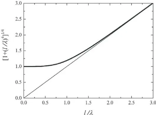
The graph of this function is shown in Fig. 2. From here, the physical meaning of the value le (or p)
becomes clear. According to Eq. (47), it is the effective half-width of an interval on they axis, on which the waveguide fields, described by singular additives in Eq. (42), increase in the process of propagation from zero (at negative y) to some stationary value (at positive y). The cause of such increase, as of appearance of waveguide modes in general, is the diffraction of incident radiation by the edges of a slot. Hence, it would appear natural to suppose that the valuele is of the order of the slot half-width.
However, if the last is much less than the wavelength, the effective half-width of diffraction region le
must be assumed not less than this length, because the scale of effects of spatial field change under diffraction is of the order of it. That is the reason to determine the effective half-width as
le= 4
Figure 2. Spatial dependence of the amplitude function in Eq. (47) for waveguide modes, propagating in the positive (solid line) and negative (dashed line) directions of the y coordinate, parallel to the boundaries of a dielectric layer.
Figure 3. Effective half-width of diffraction region le in Eq. (48), normalized on the wavelength λ, as
a function of slot half-width l.
whereλis the wavelength of the incident field (Fig. 3). In the cases when the slot half-widthl is much greater than the wavelength, the effective half-width of the diffraction region le coincides with that in
magnitude, but if ldecreases, the effective half-width becomes closer to the wavelength.
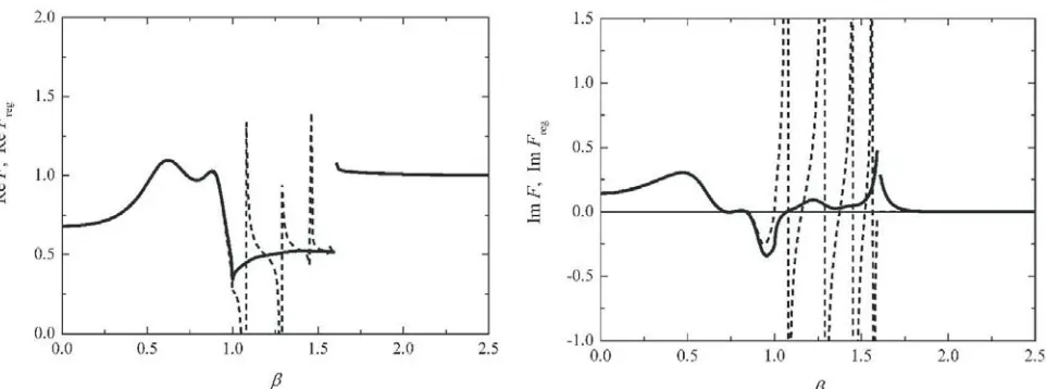
Efficiency of the extended method of singular integral regularization can be clearly illustrated by the example of two functions
F(β) = 1
D(β) and Freg(β) = 1 D(β) +
J
j=1
χj(β)
Γj (49)
(a) (b)
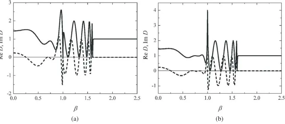
Figure 4. Variation of function D(β) in Eq. (15) with propagation parameter β for a transparent dielectric having index of refraction 1.6 and thickness h = 1.4λ, for the cases of two polarizations of field: (a) theH polarization and (b) the E polarization. Real part of a function is shown by solid line, imaginary one is presented by dashed curve. The distance between a dielectric and a screen H= 0.2λ.
Figure 5. Complex singular functionF (dashed curve) and its additive regularization Freg (solid line)
of Eq. (49) for transparent dielectric layer, placed on the distance H= 0.2λ from a conducting screen, in the case of the H polarization of propagating radiation.
Figure 6. Complex singular functionF (dashed curve) and its additive regularization Freg (solid line)
of Eq. (49) for transparent dielectric layer, placed on the distance H= 0.2λ from a conducting screen, in the case of the E polarization of propagating radiation.
Thereby, all parameters of our solution of the diffraction problem are finally determined. However, some doubts can arise here concerning uniqueness of this solution, because our choice of the parameterp (orle) in the form of Eq. (46) (or Eq. (48)) cannot be recognized as solely true and one-valued. Indeed,
we have no weighty objections against that, to do the effective half-width of waveguide modes generation region le somewhat greater or smaller than Eq. (48), which leads to change of the last summands in the
right-hand side of Eq. (45), describing waveguide mode fields. Therefore, the guided field is determined ambiguously in the near zone, i.e., in the region, where it is determined by the value of parameter le
(in the region of minor values of they coordinate). Meanwhile, the total field also includes undirected component, presented by the regular integrals in Eq. (45), whose integrands incorporate initial waveguide terms, but with the opposite sign. Thereby, the ambiguity in the determination of waveguide terms in the near zone is compensated by the same ambiguity in the determination of undirected component, hence, the total field is determined reasonably in a unique fashion. And in the far zone, i.e., in the region of great values of they coordinate (at |y| le), where the undirected scattered field decreases to zero,
a value of the parameterleno longer has effect on the waveguide mode fields. Here, they correspond to
stationary propagation of waveguide modes in a transparent dielectric layer at infinity. Else, one can pay attention to the following feature of the waveguide fields in Eq. (45): being considered separately, at small y they do not satisfy the Helmholtz Equation (1). However, here the same situation takes place as for ambiguity: the total field as a whole in Eq. (45) satisfies all requirements, because it has been constructed as a such solution initially. And in the far zone waveguide components, describing asymptotic behavior of the initial singular field integrals in Eq. (24) at infinity, satisfy all necessary conditions, including the Maxwell equations and the boundedness condition for diffraction field.
Under construction of diffraction solution, we have tried does not move beyond a contour of integration on the real axis of the parameter β, and for determination of singularities, have sought minima of the modulus of D(β) in Eq. (15) on this real axis. We have got that the parameter σj in
Eq. (34), which determines displacement of poles from this axis, also determines decay of waveguide modes in the direction of their propagation, displayed by the last sum in expression (42). We could apply more usual approach with passing on the complex plane of the argument β and determining zeroes of the function D on this plane, but not their projections on the real axis, i.e., could solve Equation (28) directly. In this case, we would get, for a dielectric layer with small absorption, that such zeroes are determined by the complex values β =βj+iσj. It gives the same result for the decay
lies wholly in the region of excitation of undirected scattered field.
As pointed above, in the presence of absorption in a dielectric layer, when its dielectric permittivity has a positive imaginary part, all minima of the functionDin Eq. (15) determine positive values of the parameters Sj in Eq. (32), and correspondingly, positive values of σj in Eq. (34). This provides decay
of the waveguide modes fields in Eq. (45) in the direction of their propagation. In accordance to such definition of signs forσj, we have determined the signs for the singular integrals in Eqs. (40) and (43).
However, in an amplifying medium, the imaginary part of dielectric permittivity becomes negative, and as a result, the parameters σj also become negative. Though this is a rare case for practice, we
must point to changes in the theory associated with this case. Firstly, the result of computation of the integral in Eq. (40) becomes the value, which is complex conjugated to the former one, i.e., instead of iπ we get−iπ. And for the integrals in Eq. (43) we should take into account the change of signs forσj,
hence instead of the result in Eq. (47) one obtains
U(y) = sgn(σj)
1 + exp[−ysgn(σj)/le]
where sgn is the signum function: sgn(t) = 1 at t≥0 and sgn(t) = −1 at t <0 (all σj have the same
sign).
Up to this point, we have not drawn special attention to the case of transparent dielectric layer, considering it simultaneously with the case of slight absorption in a dielectric. Meanwhile, in the absence of absorption, the parameter σj tends to zero, why the integral in Eq. (40), determined in the sense of
the Cauchy principal value, also tends to zero, and the integral in Eq. (43) for spatial components of waveguide fields no longer equals the value of Eq. (47). For absorbing medium, the integral in Eq. (47) describes the amplitude of waveguide mode, progressively growing in the near slot region from zero up to its maximal value, and this growth occurs in the direction of mode propagation. But at σj = 0 the
integral in Eq. (43) equals −iptanh(y/2le), which gives entirely different pattern of waveguide modes
propagation in space. Then, the fields of these modes turn out equally growing in magnitude in the both directions of the y axis, independently of their directions of propagation. It contradicts the basic conceptions of the diffraction theory, that diffraction field arises in the region of the presence of an obstacle (slot), but not at infinity. However, note that for absorbing dielectric, no matter how low is the absorption, i.e., no matter how small is the parameterσj, one obtains the wanted result in Eq. (47)
with waveguide modes, which emanate from diffraction region to infinity. That is why in the diffraction theory for transparent dielectrics one uses the following procedure: the real parameter, proportional to absorption and determining character of solution (in our case, such parameters areσj), is not taken equal
to zero, but is assumed infinitesimal positive value. Mathematically it is equivalent to the conventional rules for going round the poles for fields integrals [11] and corresponds to small shift of the contour of integration from poles [2, 20], or, what is the same, to small shift of these poles from the real axis of the argument [31]. According to this approach, the case of transparent dielectric can be considered as the limiting case σj → 0 (or Sj → 0) of a dielectric with absorption, and for this case one should use the
same expressions (45) for diffraction fields.
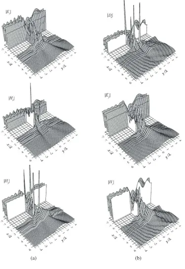
The above obtained formulas (8), (27), (45) provide calculation of the field in any point of space and represent the regularized solution of the problem of the plane electromagnetic wave diffraction by a perfectly conducting screen of arbitrary thickness with a slot and with a plane dielectric layer, placed behind it. As an illustration, we present results of computation of various spatial field components at wave diffraction for two polarizations, pictured in Fig. 7. The boundaries of a dielectric layer are not indicated in the figures, but, at least, the lower boundary of a layer displays itself as a boundary between the pattern of standing waves in a dielectric and the pattern of running waves in empty half-space [18].
4. EFFICIENCY OF WAVEGUIDE MODES EXCITATION
(a) (b)
Eq. (2) corresponding component of the given vector is
Py(x, y) = 8c
π
Re[Ez(x, y)Hx∗(x, y)] for theH polarization
−Re[Ex(x, y)Hz∗(x, y)] for the E polarization
(50)
This is inhomogeneous flux density in various points of space. To give a simpler estimation, one should determine the density, averaged over the normal coordinate x. It equals the integral of the value in Eq. (50) over all regions of waveguide mode existence (from the lower boundary of conducting screen x=dto positive infinity ofx, see Fig. 1), divided by effective thickness of a waveguide. The last value includes the whole thickness of the guiding layerh and also some part of the thickness of media nearby, because the field in these media, while decays in normal, can transfer substantial part of waveguide mode energy in the tangential direction, just as electromagnetic waves in conducting media [20]. As it is known, at exponential amplitude decay in the fashion exp(−kτ x), the effective thickness of transmitting energy layer in medium equals 1/kτ (skin depth [20]). That is why for medium 5 behind the guiding layer, where the waveguide field decays in the exponential manner, an addition to the effective waveguide thickness should be 1/kτj, whereτj is the decay coefficient in Eq. (29) of the mode with the numberj. It
has been pointed above that in medium 3, between a waveguide and a conducting screen, the field decays in the fashion of the hyperbolic sine or cosine. It would not be a big mistake to consider such decay as exponential one and to determine the contribution of this medium H(eff) to the effective waveguide thickness also as 1/kτj. However, the thickness of this region H is finite. It can be smaller than this
value, and then, naturally, one should suppose that H(eff) =H; otherwise, the given contribution can be determined as for infinite medium. Hence, the effective thickness of a dielectric waveguide can be determined by the expression
h(eff)j =h+ 1/kτj+H(eff) (51a)
where
H(eff)= 1/kτj for H >1/kτj and H(eff)=H for H <1/kτj (51b)
One should take into account that every waveguide mode of the field in Eq. (45) is presented by superposition of two modes. They propagate in opposite directions of the y axis with different amplitude coefficientsAj(β), which are determined for the values of propagation parameterβ =βj and
β =−βj, respectively. For each of them, amplitude values of practical interest are the stationary values of amplitudes on sufficiently great distance |y| from a slot, when the integral in Eq. (47) U(±y) ≈ 1 for both oppositely directed mode components. Then the last terms in the representations of Eq. (45), describing the fields of every waveguide mode, take the form
Ez(±j)(x, y)
Hz(±j)(x, y)
= εν(x)2π Γjf
+
m(βj, x)Aj(±βj) exp(±ikβjy∓kσjy) (52a)
Hx(±j)(x, y)
−E(±j) x (x, y)
= βj
2π Γjf
+
m(βj, x)Aj(±βj) exp(±ikβjy∓kσjy) (52b)
where the functions, determining its dependence on the normal coordinate x, are given by expressions (26), in which one should take into account purely imaging character of the parameters of normal propagation in air of Eq. (29). The averaged value of energy flux for every waveguide mode is obtained after substitution of expressions (52) into Eq. (50) and after integration over all x from d to +∞. The absolute value of the flow cannot serve as objective estimate, but such estimate should be determined by its relative value, normalized on the flux energy density of the incident wave in Eq. (5) in the direction of its propagation P0 = (c/8π)α−2ν. From here, we obtain the efficiency of every mode
excitation, determining the dependence on the normal coordinate in terms of its averaged relative energy flux density
where
Ij =
+∞
d 5
m=3
|f+
m(βj, x)|2dx
= τj−2νexp(−2kτjH)
4 sin2(kγjh)
1−exp(−4kτjH)
2kτj −
2(−1)νHexp(−2kτjH)
!
+2εν|T34(βj)|2 h+
sin(kγjh)
kγj Re
(R43(βj) exp(ikγjh))
!
+|T34(βj)T45(βj)|
2
2kτj
(53b)
is the integral of the square of the modulus of the functions in Eq. (26) over corresponding region of waveguide mode propagation, andh(eff)j is the effective waveguide thickness in Eq. (51) for every mode. Here, the amplitudesA(±βj) of Eqs. (17b), (25b) of modes, propagating in opposite directions of they axis, are computed as solutions of the boundary problem for the tangential propagation parameters βj
of every waveguide mode, and these parameters are determined from the condition in Eq. (30).
According to Eq. (53), the waveguide modes intensity rapidly decreases under increase of the distance between a layer and a conducting screen, and its value peaks atH= 0, when the screen directly adjoins to a layer. In this case, the waveguide structure represents a dielectric layer on the perfectly conducting substrate with a scattering obstacle (slot). Since the tangential electric field on the surface of such a substrate should vanish, the modes of this structure are the same as the antisymmetric H modes and the symmetricE modes of a solitary dielectric layer of twice as thickness [22].
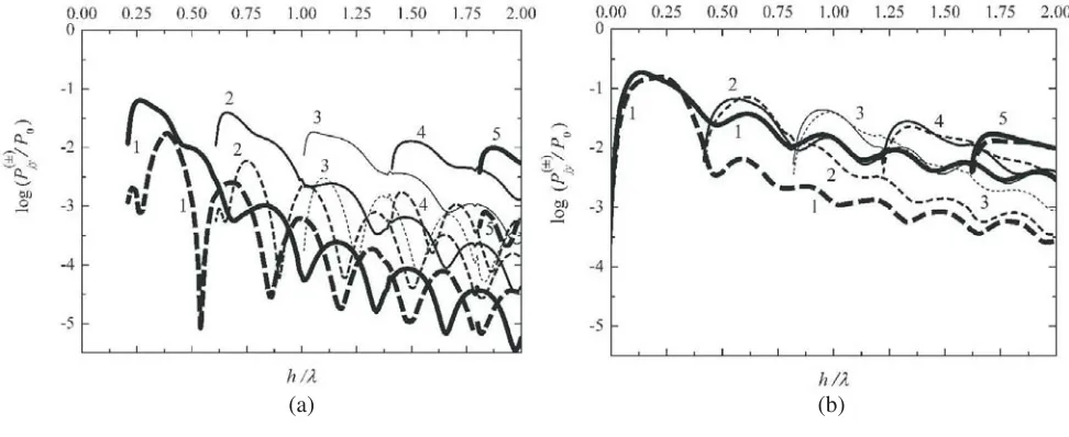
Figures 8 and 10–12 demonstrate the dependence of the relative efficiency of diffraction excitation for waveguide modes of a transparent plane dielectric layer (σj = 0) on geometrical parameters of a
problem: the thickness of a layer h, the slot half-width l, the screen half-thickness d, and the angle of initial wave incidence on a screenϑ. In these figures, the number on each curve corresponds to the mode number. It has been supposed that the screen borders to a layer (H = 0), whose index of refraction n= 1.6. Efficiency of excitation has computed by formulas (53) for waveguide modes, propagating in the positive direction of the tangentialyaxis (solid lines) and in the negative direction (dashed curves). Figure 8 is a clear demonstration of the well-known fact that the number of modes in a dielectric layer depends on its thickness. If it is small, only one mode can be excited in a layer and may be not one (see Fig. 8(a) at h < 0.2λ), but with increase of the thickness, the number of layer modes progressively increases. Upon appearance of a new mode, the intensities of the remaining modes can
(a) (b)
undergo steps of increase or decrease. In a transparent layer, they are not sharp, but in the presence of absorption, they can be great. This is evident from Fig. 9, which shows similar dependences for layers of various thicknesses with the index of absorption κ = 6.0×10⁻³ at the same values of remaining
parameters of the problem. It follows from Figs. 8 and 9 that the greatest intensity of waveguide modes is observed near cutoff, not in the point of the mode appearance in itself, but at some exceeding of corresponding values of thickness on the amount 0.1–0.2λ. A comparison between Figs. 8 and 9 shows that in the presence of slight absorption, the waveguide modes differ little in intensity from the modes of a transparent dielectric layer, with other factors being the same. Fig. 9 demonstrates appearance of an additional mode with number 6, which can exist in absorbing layers of small thickness (less than
(a) (b)
Figure 9. Relative efficiency of diffraction excitation for waveguide modes of (a) the H polarization and (b) the E polarization in an absorbing dielectric layer as a function of its thickness. Slot half-width l = 0.5λ, screen half-thickness d= 0.6λ, angle of wave incidence on a screen ϑ= 30◦. Index of absorptionκ= 6.0×10⁻³.
(a) (b)
the radiation wavelength) and is absent in a transparent layer. The value of its tangential propagation parameterβj is of the order of the index of refraction of a layer, but intensity is so small that it can be
neglected at construction of the theory.
The presented figures provide determination of the conditions of optimal excitation of waveguide modes in a dielectric layer, for which the amplitudes of these modes reach maximal values. They show that the efficiency of mode excitation by radiation of theE polarization is greater by several folds than that for theHpolarization, with everything else being equal. For the first polarization, in specific cases the averaged flux energy density can be sufficiently great, with the value of the flux density for incident field being 0.15–0.18, whereas usually the efficiency does not exceed the value of the order of 10−2–10−3.
(a) (b)
Figure 11. Relative efficiency of the slot diffraction excitation for waveguide modes of (a) the H polarization and (b) the E polarization in a transparent dielectric layer as a function of screen half-thicknessd. Slot half-widthl= 0.5λ, dielectric thicknessh = 0.65λ, angle of wave incidence on a screen ϑ= 30◦.
(a) (b)
Such great values of excitation intensity are reached, for example, at the layer thicknessh≈0.1λ, at the half-width of a slotl≈0.5λ, and at the screen half-thicknessd≈0.5λ. Generally, to reach the maximal intensity of waveguide modes, one should choose the value of the angle of incidence in the range from 20 up to 40◦ (Fig. 12), and the screen thickness must be as small as possible (Fig. 11), but the slot width should be made no less than the wavelength. At that, the choice of specific value for this width is rather arbitrary, if only it does not fall in the range of minimum intensity for a given mode (Fig. 10).
5. CONCLUSION
We have fully considered the theoretical method, developed on the basis of eigen-wave representation of the fields in partial regions, which provides a rigorous solution of the problem of diffraction of a plane electromagnetic wave by a slot in a conducting screen with a parallel dielectric layer. This method allows for application of simple techniques for calculation of singular field diffraction integrals by the way of additive regularization with explicit extraction of waveguide modes of a layer in the presence of slight absorption or amplification in it. It is fully suitable for a transparent dielectric layer, taking into account this case as a limiting one with infinitesimal absorption. The case of strong dielectric absorption can also be considered under this theory, because it gives negligibly small values of waveguide mode amplitudes due to great mismatch of scattered fields with the fields of these modes. In this case the poles of integrands are located sufficiently far away from the contour of integration, and therefore, there is no need to perform regularization of field integrals by the method of special extraction of waveguide terms.
The solution, obtained by application of the given method, can be recognized as fully rigorous, in spite of slight uncertainty of the procedure of waveguide terms extraction from the total field in the near zone, because the total diffraction field does not change at that, as well as the field of extracted waveguide fields in the far zone. Such uncertainty manifests itself in the fact that the additional terms of integrands, introduced for compensation of their singularities, can be chosen with various asymptotics at infinity of the parameter of integration (parameter of propagation of plane waves of the continuous spectrum). Thereby, the proposed method allows for adequate description as of the total field in the near diffraction zone, as of the field of guided waves of a layer in the far zone.
Computations carried out on the bases of the given method provide evaluation of the efficiency of waveguide mode excitation in a plane dielectric layer by slot diffraction at various conditions. It turns out that the efficiency of excitation by radiation of theE polarization is greater by several folds than that by radiation of the H polarization, but the greatest efficiency of such excitation does not exceed 15–18% and is attained only at several specific cases for thin layers with the thickness of the order of the wavelength and smaller, whereas usually the efficiency of excitation appears to be a value of the order of 10−2–10−3 and smaller. Therefore, the considered mechanism of diffraction excitation
of waveguide modes with the help of a solitary slot is not effective. But it does not mean that one can disregard waveguide mode fields in solving the slot diffraction problem. Neglect of waveguide modes causes mistakes in determining fields behind the screen and appreciable errors in the boundary equations, which does not allow for adequate control of the accuracy of diffraction solution for the fields.
REFERENCES
1. H¨onl, H., A. W. Maue, and K. Westpfahl, Diffraction Theory, Springer, Berlin, 1961 (in German). 2. Noble, B., Methods Based on the Wiener-Hopf Technique for the Solution of Partial Differential
Equations, Pergamon, London, 1958.
3. Weinstein, L. A., The Theory of Diffraction and the Factorization Method, Golem, Boulder, 1969. 4. Ufimtsev, P. Ya.,Theory of Edge Diffraction in Electromagnetics, Tech Science, Encino CA, 2003. 5. Hurd, R. A. and B. K. Sachdeva, “Scattering by a dielectric-loaded slit in a conducting plane,”
Radio Science, Vol. 10, No. 5, 565–572, 1975.