THERMIONIC EMISSION AND TUNNELING
Thesis by Stephen L. Kurtin
In Partial Fulfillment of the Requirements For the Degree of
Doctor of Philosophy
ACKNOWLEDGEMENTS
I would like to thank Carver Mead whose insight and enthus-iasm have served as stimuli for this research; my wife, Barbara, whose understanding of the way in which the world, ·and her husband in
ABSTRACT
Current flow in metal-GaSe-metal sandwiches is investigated. These structures are particularly well suited to the study of current flow mechanisms because sandwiches containing uniform, single crystal films of gallium selenide can be easily fabricated. The well-defined nature of these structures allows sufficient ~ priori knowledge of their properties to make quantitative calculation of the predictions of
appropriate models of current flow meaningful.
As discussed in Part I, for gallium selenide films between
0 0
200 A and 1000 A thick, experimentally observed currents are in excellent agreement with a simple model of thermionic contact-limited current flow. This investigation presents the first unequivocal evidence for contact-limited thermionic currents in solids.
0
ACKNOWLEDGEMENTS ABSTRACT
TABLE OF CONTENTS
I THERMIONIC CONTACT-LIMITED CURRENTS I.l Introduction
I.2 Background
I.3 Properties of Gase I.4 Sample Preparation I.5 Bulk Limitations
I.6 Contact-Limited Transport
I.7 Barrier Shape and Carrier Distribution I.8 Conclusion
I.A Appendix I.R References II TUNNELING CURRENTS
II.l Introduction
II.2 Theory of Tunneling in MIM Structures II.3 Experimental Considerations
A. Gallium Selenide
B. Fabrication of MIM Structures C. Preliminary Calculations D. Measurement Technique E. Selection of Structures II.4 Results and Interpretation
A. Al-GaSe-Au Structures
B. The E-k Dispersion Relation
C. Energy Distribution of Tunneling Electrons
II.5 Conclusion II.R References
i i i i i
PART I
THERMIONIC CONTACT-LIMITED CURRENTS
I.l INTRODUCTION
In this part we review the basic physics of contact-limited current flow and apply a simple model to the analysis of data obtained on well-defined MIM structures incorporating single crystal gallium selenide as the thin insulating film. The bulk and interface properties of gallium selenide were determined by independent experiments; these properties were used in the calculation of theoretical currents. No adjustable parameters were required. Both the magnitudes and functional dependencies of observed currents are in excellent agreement with
theo-retical predictions. Experimental variables include voltage, temperature, and insulator thickness. We believe that the excellent quantitative
agreement obtained between theory and experiment provides the first un-equivocal evidence for thermionic contact-limited transport in solids.
compares the results of numerical calculations with experimental data obtained on Al-GaSe-Au structures. Excellent agreement is noted.
Section I.7 presents direct evidence for image-force (Schottky) barrier lowering. In addition, this section includes a discussion of the
I.2 BACKGROUND
Contact limited emission was first studied for the metal-vacuum interface. In this case three mechanisms of current flow may be distinguished:
1. Thermionic emission1 (Schottky emission) occurs in the low field, high temperature limit and is a flux of electrons on the high-energy tail of the Maxwell-Boltzmann distribution over the image-force-lowered work function barrier.
2 • F . 1e ld emission . . 2 ' 3 ( F ow er- or eim tunne ing 1 N dh ' 1 . ) occurs in . the high-field, low-temperature limit and is the direct quantum mechan-ical tunneling of electrons from allowed states below the Fermi level in a metal into allowed states in the vacuum.
3. Thermal-field emission4-7 (T-F emission) occurs when the dominant contribution to the observed currents arises from the tunnel-ing of thermally excited electrons through the narrow upper region of the image-force-lowered work function barrier. This mechanism of current flow is intermediate between thermionic emission and field emission.
8
To gain insight J.nto the phys:ic::1 of c.llrrier transport, one muy ul.Ho
numerically evaluate the relative contribution to the current of currlers
with various energies. Such energy distributions are considerably more
informative than a mere classification of transport phenomena into the
three cases outlines above.
Of course, even in metal-vacuum-metal structures, currents
are not always contact limited. When more electrons are present in the
vacuum region than can be collected in a transit time, build up of free
charge in the vacuum region leads to the familiar space-charge-limited
conduction in which the virtual cathode is spatially displaced from the
physical cathode.
As interest in solids developed, it was natural to attempt
analysis of current flow in solid state MIM structures. However, solid state insulators are far more complex than a vacuum and many additional
factors must be taken into consideration. Two types of considerations arise:
a) the fundamental parameters of the insulator (e.g. carrier
effective mass and dispersion relationship, dielectric constants,
mobility-field relationship, interface barrier energies, trap densities
and locations, etc.) must be known if meaningful predictions are to be
made;
b) experimental techniques for preparing reproducible
structures suitable for detailed study must be evolved.
These two types of considerations are not independent since values
from the results of measuremt:!ntn on experimental H true tureH.
Samples are usually fabricated by oxidation of a de.pmdted metal film or by similar techniques. These techniques yield amorphous insulating films whose properties are ill-defined at best and are often spatially non-uniform. Current flow observed in such structures ex-hibits a generally exponential dependence on applied voltage and is
9-11
often temperature dependent. Since the bulk and interface proper-ties of such insulating films are not known in detail, a rigorous matching of observed currents with a given model of carrier transport has not been possible. The usual procedure is to study the dependence of current on one or more variable (e.g. applied voltage, temperature, insulator thickness, electrode material, etc.), surmise an appropriate carrier transport mechanism or model, and then choose the parameters of the model (in fact these parameters are physical properties of the in-sulating film) so that the "predictions" of the model fit the observed currents. Great caution should be exercised when following such a procedure since physically distinct phenomena can lead to qualitatively
. ·1 b h . 11
I.3 PROPERTIES OF Gase
Gase, used as the insulating material in all experiments
13
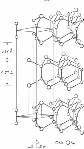
reported here, is a l~yier compound having the crystal structure shown
in Fig.
I.I.
This structure consists of tightly internally boundfour-fold (Se-Ga-Ga-Se) layers, stacked one on top of another to form a macro
crystal held together by Van der Waals forces. As a result of this
bonding configuration, it is possible to fabricate by peeling techniques
thin film .. s tructures in which the single crystal character of the
resulting GaSe thin film is maintained. Therefore, the properties of
the Gase film which is thus incorporated within a metal-Gase-metal
structure are necessarily identical with those of bulk Gase crystals.
The ability to incorporate a single crystal thin film in MIM structures
permits interface, bulk, and thin film measurements to be performed on
one and the same well-defined material.
To characterize the bulk properties of GaSe, several experimental
techniques have been employed. Dielectric constants have been determined
14
by both low-frequency and infrared measurements. Capacitance
measure-ments on thin, fully depleted samples indicate the low-frequency dielectric
constant Kdc
=
8.0 ± 0.3 for the electric field parallel to the c-axis(e
I I
c). Analysis of infrared reflectivity for each polarization ofthe electric vector yields Kopt
=
7.1, Kdc=
7.6 fore
I
I
c; andK t op
= 8.4, Kd
= 10.2 for
'€
c. Multiple interference channeledC L
spectra imply K t = 7 .45 and Kd = 9.89 for
.
_eL
c.op c
T:
3.17 A
t
4.77 A
l_
OGa
Ose
Fig. I.l Schematic representation of the layer compound Gase (after H. Kumimura and K. Nahao, Ref. 13). The tightly bound
four-fold (Se-Ga-Ga-Se) layers are 4.77 ~ across and are held together at an interlayer separation of 3.17
X
by pre-dominantly Van der Waals forces. This material cleaves easily perpendicular to its c-axis thus facilitating the [image:11.615.180.466.103.610.2]From measurements of capacitance as a function of voltage, our material
was determined to be p-type with p 3 x 1014 cm-3 at room temperature.
Ab sorpt one ge measurements i d 15 in icate t a t t e . d. h h b an gap is d 2 0 . eV.
In addition, photoresponse measurements at photon energies less than
th e b an gap y1e d . ld sur ace arrier energies f b . . 16 ( . i.e., t e energy o h f t e h
metal Fermi level above the Gase valence band): Al-Gase, ¢Al= 1.05 eV;
Au-Gase, ¢Au = 0.52 eV.
The relative importance of trapping states in bulk GaSe samples
was appraised by determining (at constant applied bias) the sensitivity
to broad-band optical radiation of the capacitance of metal-semiconductor
interfaces (Schottky barrier depletion layer). No measurable change in
capacitance was observed for the specimens used in this series of
experi-ments1~ ialthough material from highly doped (p ~ 10 18 cm -3 ) boules gave
evidence of severe bulk trapping. In addition, measurements of
capaci-tance as a function of frequency, performed on these same interfaces,
failed to reveal any lifetime-dependent phenomena. This evidence for
the absence of dominant bulk trapping indicates that NT << p.
Tunneling measurements performed on metal~GaSe-metal structures
0
incorporating a Gase film less than 100 A thick indicate that the tunneling
effective mass for carriers near the valence band edge is approximately
0.1 of the free electron mass. Data obtained from tunneling experiments
are qualitatively different17 from those for the thicker films discussed
18
I.4 SAMPLE PREPARATION
Experimental structures used in this investigation were
constructed by the following technique:
0
1) Approximately 1000 A of metal (typically aluminum) was
vacuum evaporated on one side of a freshly cleaved GaSe
flake (~ 5µ thick).
2) The flake was then mounted, metal side down, on a brass
block. A 100% solids, silver loaded epoxy was used both
to bond the flake to the block and to provide electrical
contact to the evaporated metal layer.
3) The Gase flake was peeled, in air, 19 to a thickness t
0 0
(150 A < t < 2000 A; i.e., 20 to 250 integral Se-Ga-Ga-Se layers) by application of a flexible adhesive tape (Scotch
Magic Transparent Tape) to the exposed upper Gase surface.
Care was taken to assure that a continuous Gase film was
removed with each successive peeling step, thereby
elimi-nating the possibility of gross surface contamination by
the tape adhesive.
4) Counterelectrodes of a metal (typically gold) were formed
by vacuum evaporation through a fine mesh onto the freshly
exposed (0001) surface. Each separate metallic dot defines
an individual Al-Gase-Au structure.
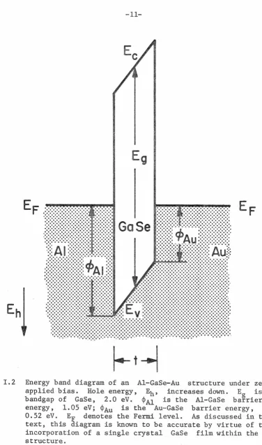
A schematic energy band representation of a typical (Al-Gase-Au)
structure is shown in Fig. I.2. By virtue of the incorporation of a single
Eg
Fig. I.2 Energy band diagram of an Al-Gase-Au structure under zero applied bias. Hole energy, Eh, increases down. Eg is the bandgap of Gase, 2.0 eV. ¢Al is the Al-Gase barrier energy, 1.05 eV; ¢Au is the Au-Gase barrier energy,
[image:15.614.143.520.81.720.2]I.5 BULK LIMITATIONS
In the absence of direct tunneling between the metal electrodes,
current transport through MIM structures involves two serial processes.
Carriers are injected into the insulator at the metal-insulator
inter-face; they then traverse the insulating region. Either process can in
principle limit the current. However, it is possible to define some
criteria which, if fulfilled, insure that bulk limitations are not
dominant. Bulk-limited currents can arise via two mechanisms: space
charge and scattering (including for our purposes shallow trapping and
other processes yielding low effective mobility).
Space charge limitations dominate carrier transport in MIM
structures when the amount of uncompensated charge in the insulating
region is sufficiently large to terminate a significant fraction of the
field lines emanating from the metal electrodes. Both mobile charge
(i.e., carriers in transit) and trapped charge contribute to this
un-compensated charge. The mobile charge Q present in an insulator due
to a current I is given by Q = IT, where T is the time required
for a charge carrier to transit the insulating film. If this charge is
much less than the charge on the metal electrodes given by Q electrode
CVT' where C is the capacitance of the structure and VT is the
total voltage across the insulator (applied plus internal}, then the
space charge due to the mobile carriers is negligible. This condition
is expressed by the inequality
An upper bound on the contribution of trapped charge can he obtained from the total number of traps and the (worst case) assumption that all traps are ionized. Again, the criterion for neglecting the trapped space charge is t~at tt be small compared to the total charge on the metal electrodes. The inequality
(I. 5-2)
where e is the electronic charge, Nt is the density of traps, t is the thickness of the insulator, and A is the area of the structure, expresses this condition.
In those cases where the charge carriers traverse the insulator against the field before encountering the limiting barrier, both trapping and strong scattering may lead to deviations from the simple ballistic model of current transport discussed below.
If none of these mechanisms for bulk current limitation is present, the current will be contact--limited.
As noted in Section I.4, the GaSe film incorporated within a Au-GaSe-Al structure is single crystal material having the properties of bulk specimens. Thus, the criteria for observing contact-(as opposed to bulk) limited current can be checked in detail. For our material the number of traps is less than the acceptor density (as discussed in Section I.3) and hence the effect of the space charge due to ionized acceptors and deep traps can be estimated from the acceptor density. For p ~ 3 x 10 14 cm -3 and
0
t ~ 500 A, the change in potential across 2
may thus be neglected.
The influence of space charge associated with current carriers in transit can be assessed on the basis of inequality I.5-1~ By using data from experimental current-voltage characteristics and the structure capacitance, we may estimate an upper hmmnd (Tub) on the value of the transit time for which space charge limitations are important, i.e., Tub
=
CVT/I. For a typical sample (the sample discussed in detail later in this section), Tub varies quite widely. However, (except forbiases in the transition region from low forward to high forward where the
field
is nearly zero) the inequality is easily satisfied forphysically reasonable values of effective carrier mobility. To illustrate this point, it is useful to express T in terms of an effective mobility
2
µeff: T
=
t /µeff Vt and to use the inequality T < Tub as a criterion0
for a lower bound (µ eff) on the effective mobility. For
greater than this lower bound, charge associated with carriers in transit will not limit current flow. We find directly
(I.5-3)
For samples discussed in this paper is of order 1. Since µ 0 eff becomes large for large I and small VT' we will choose a "worst" case close to flat band: VT = 0.1 volt, I = 10 -6 amp. Therefore,
0 -4 2
µ eff ~ 10 cm /volt-sec; a value much below that expected for this material even perpendicular to the layers. Thus, currents observed i.n
possible exception of forward biases within 0.1 volts of ¢Al - ¢Au"
Within 0.1 volts of ¢Al - ¢Au' the total internal field IH Hmall
I.6 CONTACT-LIMITED TRANSPORT
A. Barrier Shape
An important consideration in any discussion of contact-limited
current is the assumed shape of the barrier potential. Simple discussions
assume the barrier to be trapezoidal in shape, neglect the influence
of space charge in the insulator, and correct the barrier shape for
single or multiple image charges induced in the metal electrodes. In
this approximation, including multiple image charges, the barrier
poten-tial is given by4
<P (x)
87TK etE t
f:
op o n=l
where I t is the optical dielectric constant of the insulator; t is op
the thickness of the insulating layer, ¢
1 and
¢
2 are the barrier energies, 20and V is the applied voltage. Except for the small range of biases
where the electric field in the barrier region is very nearly zero, charge
transport is limited by the energy barrier at one of the metal-insulator
interfaces (i.e., the limiting barrier). Consequently, approximations
to the barrier potential which are accurate near the limiting barrier
are appropriate to the discussion of contact-limited current. For
definite-ness, let us take the limiting barrier to be ¢
1, and hence consider Eq.
I.6-1 for x near zero. In the appendix we show that in this region
the multiple image-force correction (the fourth term in Eq. I.6-1) may
21
¢(x)
=
¢0 -ex -
16TIKe x opt o(I.6-2)
where we have introduced ¢
0 for the limiting surface barrier energy
and
€
for the total field acting near the limiting barrier.B. Contact-Limited Current-Voltage Characteristics
In general, the total injection-limited current is the
alge-braic sum of four contributions: both holes and electrons may flow from
either metal to the other. The relative importance of each of these
contributions can be easily assessed using a simple thermionic model of
carrier transport. To be specific, let us refer to the energy band
diagram of Fig. I.2 wherein the electrode materials are gold and aluminum.
Consider the case in which a negative bias V is applied to the gold
electrode. (Other bias conditions may be discussed in an analogous
manner). The hole current from Au-to-Al is proportional to exp[-(¢A1+v)/kT]
while the hole current from Al-to-Au is proportional to exp(-¢A1/kT).
Therefore, the ratio of the Au-to-Al hole current to the Al-to-Au hole
current is equal to exp(-V/kT). Thus, for V greater than a few kT we
can neglect the current contribution due to hole transport from Au-to-Al.
Similarly, we find that for V greater than a few kT we can neglect the
current contribution due to electron transport from Al-to-Au.
To assess the relative importance of hole current and electron
current, we may use the same simple model. The dominant electron current
is proportional to exp[-(E -¢A )/kT], where E is the band gap of the
g u g
insulator; the dominant hole current is proportional to exp(-¢A
Therefore, the ratio of hole current to electron current is given by
exp[-(¢Au+¢A1-Eg)/kT]. Thus, for jcpAu+cf>Al-Egl>kT either hole or
electron current must dominate. If (¢Au+¢A1-Eg)>O, electron current
dominates; i f (¢Au+¢A
1-Eg.)<O, hole current dominates.
In summary, if both the applied bias and the quantity
l¢Au+cf>A1-Egl are greater than a few kT then the major contribution to
the total injection limited current comes from one and only one of the
four possible contributions. Throughout the remainder of this paper,
the above criteria will be satisfied for applied biases greater than 0.05
volt, since l¢Au+cpA
1
-Eg1~ 0.4 eV >> kT (kT ~ 0.025 eV at room temperature).The current-voltage characteristic of an asymmetric (¢Au<¢A1)
MIM structure in which current flow is contact-limited depends on two
factors: the source of the current carriers, and the barrier which
limits current flow. These two factors lead to a natural division of
the current-voltage characteristic into three distinct regions depending
upon which energy barrier is limiting current flow and which metal is
supplying most of the current carriers. As illustrated by the solid
curves and insets of Fig. I.3, these three distinct cases are "low
forward," "high forward," and "reverse." Using the definition that
positive bias results in-aurrent flow from gold to aluminum, we define
the various cases in the following manner. Low forward occurs when
positive bias is less than ¢A1-¢Au· In this case the limiting barrier is
the ¢Al barrier, the source of the current carriers is the gold electrode
and current flows against the internal field. For the low forward, the
Al-Go Se-Au
t=sooA
• EXPERIMENT - THEORY
·LI
Fig. I. 3
Fig. I.3 Current-voltage characteristic of an Al-Gase-Au structure.
Both directions of applied bias are shown on this figure.
The dots are experimental data; the solid line is numerically
calculated from the theory of thermionic contact-limited
current
(Eq.
I.6-3) using parameters detennined from priorexperiments on bulk GaSe (no adjustable parameters were
employed). Excellent agreement between theory and
experi-ment is evident. The insets show partial band diagrams of
the Al-Gase-Au structure and illustrate the bias
condi-tions we denote "low forward": 0 <
v
< (¢Al - ¢Au);"flat band":
v
=
(¢Al -, ¢Au) ; ''high forward":V > (¢Al - ¢A); and "reverse": V < 0. This descriptive notation is helpful when discussing thennionic
contact-limited current flow because for a given structure it
conveys a knowledge of the direction of current flow, the
on applied bias since the limiting barrier (¢A1-v) decreases linearly
with voltage. In the absence of scattering and direct carrier tunneling,
1
the slope of the log I vs. V curve is very nearly kT High forward
occurs when the applied bias is positive and greater than ¢A1-¢Au· In
this case the limiting barrier is ¢Au' and the source of the current
carriers is the gold electrode. Image lowering of ¢Au and contributions
to the current from thermal-field and field emission mechanisms cause the
observed increases in current with increasing bias. Reverse occurs when
the applied bias is negative. In this case the limiting barrier is ¢Al'
and the source of the current carriers is the aluminum electrode. The
increase in current with increasing bias observed in this case is a
result of barrier lowering and tunneling, the same mechanisms which
operate in the high forward.
The solid curves of Fig. I.3 are the theoretical current-voltage
0
characteristic of an Al-Gase-Au structure incorporating a 600A single
crystal film of Gase. These curves were numerically calculated using
the known properties of GaSe (see Section I.3) and a theoretical model
(discussed below) of thermionic injection-limited currents adapted from
8 22
the treatment by Murphy and Good ' of the metal-vacuum interface.
In general, the expression for current as a function of applied
voltage consists of the integral over all energies of two factors: a
supply function which gives the flux of carriers from the source electrode,
and a transmission function which gives the probability that a carrier
incident on the limiting barrier is transmitted through it. In the
component of the carrier's energy normal to the metal-insulator interface
and on the applied bias (via the electric field
e>,
the current may bewritten as
(I.6-3)
where E~ is the component of the carrier energy which is perpendicular
to the plane of the interface and V is the applied bias. P(E~,V)
N(E~,V) are the transmission and supply functions, respectively. The
limits on the integral in eqn. I.6-3 are such that all the contributions
8 to the current are taken into account. Following Murphy and Good, we
23
assume that the metal may be described by a single parabolic band with
*
by24,25effective mass m In this case the supply function is given m
*
4Trm
{
-/3[E-EF(V)]}
N(E,V) __ m_
A
ln
l+e (I. 6-4)Sh 3
where
A
is the area of the sample, EF is the Fermi energy of the metal1 . h . 26 d
supp y1ng t e carriers, an f3
=
l/kT.In determining the dependence of the transmission function on the
perpendicular component of the energy two cases must be distinguished.
In the first case, the carrier has a perpendicular energy which is
greater than the maximum in the limiting barrier (eqn. I.6-2), and the
27 transmission function (neglecting possible reflections at the interface )
is taken to be one. In the second case, the carrier has a perpendicular
tunnel through a portion of this barrier if it is to contribute to t11e
current. If the behavior of the carrier for energies lying inside of
*
the forbidden gap is adequately described by an effective mass m.1
8 then following the derivation of Murphy and Good
(I.6-5)
~
where y
=
(ee/4nK t£) 2/(¢ -E..L). Physically, y is the ratio of the op o o
image lowering of the barrier energy to the difference between the per-pendicular component of the carrier energy and the surf ace barrier energy ¢ . The function v(y) is given by28
0
v(y)
=
2-~(l+a)~lE(~)~
-(1-a)K(le_)~'
l+a l+a ~ (I.6-6)
where a
=
~l-y
2 , andR
andE
are complete elliptic integrals of the first and second kind, respectively.From the discussion of sections I.3, I.4 and I.S, we know that our experimental structures correspond to the energy band diagram of Fig. 2 and hence that the previous discussion of the ideal MIM structures is directly applicable. We therefore expect that experimental current-voltage characteristics should correspond to the results of theoretical
calculations based on this band diagram. The theoretical current-voltage characteristic (solid line) appearing in Fig. I.3 has been calculated29 for an Al-Gase-Au structure 6.21 x 10-S cm2 in area and incorporating a
0
[image:27.614.110.549.137.528.2]of eqn. I.6-3 using the previously measured properties of bulk Gase (see Section I.3). The solid black dots which also appear in Fig. 3 are data measured on a structure having a gold counterelectrode area 6.21 x 10⁻⁵ cm2 and incorporating a 600A thick Gase film. (Film
thickness is determined directly from the electrode area and a measure-ment of structure capacitance at zero bias: t
=
Kd € A/C). Excellentc 0
agreement between theory and experiment is evident from the figure. This agreement, in and of itself, gives strong support to the contact-limited transport model. Other predictions of this model must now be investigated.
C. Temperature Dependence
For external conditions such that both thermal-field emission and field emission are negligible the simple model of thermionic contact-limited current flow predicts that (at fixed applied bias) current should
-¢
0/kTbe exponentially dependent on temperature: I ,_ e , where
¢
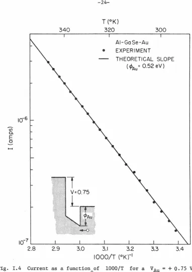
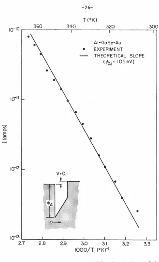
is 0the effective barrier energy limiting current flow. To confirm the thermionic origin of the currents observed in Al-Gase-Au structures, it is necessary to experimentally check these predictions. Data obtained from such measurements are shown in Figs. I.4 and I.5. Values of applied bias were chosen such that current was limited either by the Al-Gase barrier or by the Au-GaSe barrier.
From the inset of Fig. 4, it is clear that the slope of a line drawn through the data points should yield a value for the effective barrier height associated with the GaSe-Au interface. Evaluation of
this experimental slope gives
¢
=
0.514 eV which differs only slightly340
u;-0. E 0
300
Al-Go Se-Au
• EXPERIMENT
THEORETICAL SLOPE
( cf>Au = 0.52 eV)
ICJ7--~~--~----~---~---~---~---Fig. I. 4
2.8 2.9 3.0 3.1 3.2 3.3 3.4
1000/T (°Kr
1 [image:29.613.128.510.99.639.2]from the .52 eV value found by 1>hotoresponse experLmentH performed on bulk specimens. This slight deviation is due to lowerjng of the effec-tive barrier which results from both the image-force and thermal-field emission. For larger biases (higher fields) this effective lowering becomes even larger.
From the inset to Fig. I.5, it is clear that the slope of the line of data points should yield a value for the effective barrier energy associated with the Gase-Al interface. Evaluation of this slope gives ~ ~o = 1.02 eV, compared with the bulk photoresponse value of 1.05 eV. Image-force lowering (which is larger in this case than in
the case discussed above because of the built-in field) accounts for a deviation of 0.046 eV.
For a comparison of observed behavior with detailed theoretical predictions, the solid lines plotted in both Fig. I.4 and Fig. I.5 were numerically computed directly from Eq. I.6-3. This calculation takes into account the entire distribution of carriers and hence the theoretical curves in Figs. I.4 and 1.5 deviate slightly from the perfectly straight lines predicted by a purely thermionic model. As is evident from the figures, the agreement between theory and experiment is excellent. The
corres-pondence between the barrier energies measured by photoemission experiments on bulk Gase specimens and those measured thermally on MIM structures
U> a. E .,g ...
Fig. I. 5
10-10 r--3...,610 _ _ _ _ 3,4_0 _ _ _ _ __:_32;:.0=--_ _ _ _ _:3~0;:..:;0
•
Al-Go Se-Au
• EXPERIMENT
THEORETICAL SLOPE
(¢Al= 1.05 eV)
•
10-13 ~---....i.---1---L---L----..l.----L__J
2.7 2.8 2.9 3.0 3.1 3.2 3.3
1000/T (°Kt1
Current as a function of 1000/T for a VAl
=
0.1 V (reverse) biased 600i
thick Al-Gase-Au structure. The dots areI. 7 BARRIER SHAPE AND CARRIER DISTRIBUTION
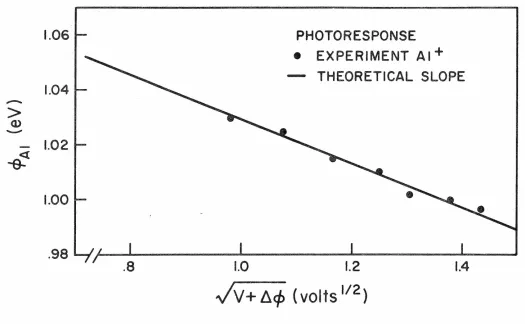
A. Photoresponse Measurements
30
The photoresponse technique is perhaps the best method of
determining interface barrier energies on bulk specimens. We have
applied this technique to MIM structures to directly investigate the
electric field dependence of the interface barrier energy. Results of
this investigation unambiguously established the barrier potential to
be in fact as deduced in Section I.6.
In the absence of appreciable tunneling,31 photoresponse
threshold (viz,
¢
)
is the energy difference between the Fermiphoto
level in the source metal and the maximum with respect
to
x of thebarrier potential. Solving Eq. I.6-2 for its maximum yields
(I. 7-1)
This result is the well-known Schottky Jl.tmwerihg in which the effective
interface barrier decreases as the square root of the total field
S,.
Data obtained from photoresponse measurements performed on
the same structure whose current-voltage characteristic appears in
Fig. I.3 are presented in Fig. I.6. For a given applied bias, the
barrier energy ~Al was obtained from the intercept of a plot of the
square root of photoresponse per incident photon as a function of
30
photon energy. The voltage dependence of ~Al was obtained directly
•
EXPERIMENT Al+
THEORETICAL SLOPE
.
~1.04
,.._
>
Q)...
1.02
4:
1.00
L
~
I
.98
.8
1.0
1.2
1.4
,./v
+
~</:>
(volts
112
)
Fig. I.6 Dependence of the effective Al-GaSe barrier energy on applied bias.
To facilitate comparison with theoretical predictions of Schottky lowering
(see Eq. I~2-l) the barrier e~ergy
,
¢Al
is plotted vs. the square rootof total internal bias: V +(~Al - ~Au). The correspondence between
theory and experiment confirms that the barrier energy exhibits Schottky lowering and is strong evidence that the barrier potential is, to good approximation, trapezoidal.
I N
co
[image:33.792.104.629.127.451.2]Schottky lowering predicted by the image-force correction to the barrier potential.
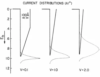
B. Carrier Distributions
Having thus established that the actual barrier potential is well described by the simple Schottky model, we can use the
contact-limited transport theory of Section I.6 to gain insight into the de-tailed mechanisms of current flow.
Results of detailed numerical calculations, specifically for
0
the case of the 600 A thick sample discussed above, are plotted in Fig. I.7. For each applied bias the solid curves illustrate the actual image-force lowered barrier potential; the dotted curve represents the
(normalized) relative contribution per unit energy to the current of carriers with a given value of E~. The extent to which any given carrier injection mechanism contributes to the observed current under a specific set of external conditions can be seen directly. As illus-trated by this figure, the dominant mechanism of current transport shifts continuously, with increasing internal field, from thermionic
0
.2
.4
ufl
.6
.8
1.0
1.2
Fig. I. 7
CURRENT DISTRIBUTIONS (Al+)
IOOA
-.f
i.-...
...
:
·:::.
·::.
~ ~"'V=O.I
...
...
..
···
.
···
V=l.O
..
·...
V=2.0
[image:35.613.127.533.160.473.2]I.8 CONCLUSION
Current flow in metal-insulator-metal structures is often very complex. In many cases physically distinct mechanisms can lead to
qualitatively similar current-voltage characteristics. Interpretation of experimental observations is particularly difficult when the proper-ties of the insulating layer are unknown. Hence, great care must be taken to avoid translating a lack of knowledge of the parameters of a structure into ambiguities about the physics of carrier transport. Many potential difficulties can be avoided if the parameters of an experi-mental structure are known from measurements which are independent
of those performed to study current flow. With such a structure the physics governing current flow can be studied in detail because quan-titative tests of the predictions of a given physical model are feasible.
In this study we have fabrieated MIM structures containing single crystal films of the layer compound gallium selenide. Prior experiments on bulk specimens of single crystal gallium selenide provide data with which both the applicability and predictions of various models of current flow can be calculated. On the basis of such calculattons we were able to deduce that space charge limitations would be unimportant
and to anticipate thermionic, contact-limited currents. Extensive measurements performed on the MIM structures are in excellent
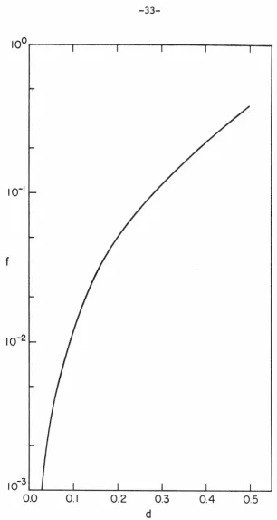
I.A APPENDIX
Multiple image-force corrections to the barrier shape should be considered in a discussion of contact-limited current only if they
significantly change the shape of the barrier potential near that con-tact which is limiting the current. For samples with insulating layers which are thick enough to rule out the possibility of a significant con-tribution to the total current from direct tunneling o.f carriers from one
0
metal electrode to the other (t ~ 150 A), and for electric fields which are large enough to define one barrier as the limiting barrier, the
in-f luence of multiple images is quite small. To illustrate this point consider the deviation, ~~(x), of the multiple image-force-corrected barrier potential from the single image-force-corrected barrier for x values near the limiting electrode. tiHx) is given by (See Eq;;_ I.6-1)
0
M(x) = e f (d) 7.2 eV-A f (d) (A-1)
8'ITK £ t K t opt 0 opt
where
00
i
f (d) =
l:
(A-2)2 2 ia=l n(n -d )
and d = x/t. In Fig. I.8 we have plotted f(d) for d in the range
0 to 0.5 (for d greater than 0.5, we should correct the barrier
shape for the image in the second electrode). This figure demonstrates
f
I0-3...._.1..-__ _._ ______ , r , . _ _ _ _ _ _ . _ _ _ _ _ _ _ . _ _ _ _ _ _ _ _ _ _ _ _
0.0
0.1 0.20.3
d
0.4
0.5
Fig. I.8 Dependence of the function f (see appendix) on the
normalized distance d. This function measure the relative
[image:38.615.166.473.92.667.2]Thus, a crude upper bound for the contribution of multiple images to the barrier shape can be obtained by evaluating the numerical.factor
multi-0
plying f (d) in Eq. A-1 for typical values of K (=7)
opt and t(= 200 A); this yields
-3
~~ < 3.6 x 10 eV •
(A-3)
I.R REFERENCES
1. W. Schottky, Physik
z.
15, 872 (1914).2. L. W. Nordheim, Proc. Roy. Soc. (London) Al21, 626 (1928).
3. R. H. Fowler and L. W. Nordheim, Proc. Roy. Soc. (London) All9, 173 (1928).
4. A. Sommerfeld and H. Bethe, Handbuck der Physik, ed. by H. Geiger and K. Scheel (Verlug Julius Springer, Berlin, 1933), Vol. 24, No. 2. 5. E. Guth and J.C. Mullin, Phys. Rev. 61, 339 (1942).
6. W.W. Dolan and W. P. Dyke, Phys. Rev. 95, 327 (1954).
7.
W.
P. Dyke, J. P. Barbour, E. E. Martin, and J. K. Trolan, Phys.Rev. 99, 192 (1955).
8. E. L. Murphy and R. H. Good, Phys. Rev. 102, 1464 (1956).
9. P. R. Emtage and W. Tantraporn, Phys. Rev. Letters ~' 267 (1962).
10.
c.
A. Mead, Phys. Rev. 128, 2088 (1962).11. J. J. O'Dwyer, J. Appl. Phys. 11_, 599 (1966).
12. See for example: J. G. Simmons, Phys. Rev. Letters 15, 967 (1965);
P. Mark and T. E. Hartman, J. Appl. Phys. 39, 2163 (1968). 13. H. Kamimura and K. Nahao, J. Phys. Soc. Japan 24, 1313 (1968). 14. P. C. Leung, G. Andermann, W. G. 8pitzer, and C. A. Mead, J. Phys.
Chem. Solids!:]_, 849 (1966).
15. P. Fielding, G. Fisher and E. Mooser, J. Phys. Chem. Solids~' 434
(1959).
16. S. Kurtin and
c.
A. Mead, J. Phys. Chem. Solids 29, 1865 (1968).17. G. Lewicki and C. A. Mead, Phys. Rev. Letters 16, 939 (1966).
18. SeeKalscH S.1 :Kurtin,:'T.iC. McGill 4\ndlC.,A.~dl(ead, Phys.Rev.Lett.
19. Previous work indicates that surface barriers prepared on Gase are not sensitive to whether the GaSe is cleaved in vacuum or in air
(see Ref. 26).
20. All energies and potentials throughout this discussion are measured in eV. All other units are MKS.
21. The appendix defines criteria for neglecting the multiple image-force correction. For a detailed discussion of various approxi-mations to the multiple image-force correction, see J. G. Simmons, J. Appl. Phys. 39, 1793 (1963).
22. Such adaptation has been previously discussed by several authors. See for example: W. Tantraporn, Solid State Electronics]_, 81 (1964). R. Stratton, Solid State Electronics~' 175 (1965).
23. The question of what effective mass to use has been discussed by several authors. See for example: Ref. 21 and also C. Crowell, Solid State Electronics~, 395 (1965). Since small deviations in the value of pre-exponential factors do not affect the qualitative character of the physics being studied we choose to use a con-ceptually simple model uncluttered by experimentaly indeterminate quantities.
24. R. Fowler and E. A. Gugenheim, Statistical Thermodynamics (Cambridge Press University Press, New York, 1952), p. 460.
25. In the low forward (see Fig.I~B) carriers traverse the insulating region against the electric field before encountering the limiting barrier. Hence for the low forward, the assumed form of the supply
slight deviation of calculated currents from those experimentally observed in the low forward.
26. The voltage dependence of the Fermi energy indicated in Eq. II6-4 calls attention to the possible variation of this energy with respect to the energy zero as the applied bias is changed.
27. Recently some authors have addressed themselves to the problem of correcting for reflections at the metal-semiconductor interface (in Schottky barrier diodes). See for example C.R. Crowell and S. M. Sze, J. Appl. Phys.]]_, 2683 (1966); C. R. Crowell, Solid State Electronics~' 395 (1965), Solid State Electronics 12, 55 (1969). However, since reflection leads only to a change in the pre-factor multiplying the current, experimental attempts to verify
the modification due to reflection have proven to be exceedingly difficult.
28. R. E. Burgess and K. Kroemer, Phys. Rev. 90, 515 (1953).
29. The effective mass of electrons in either metal is taken to be one throughout these calculations.
30. C. A. Mead, Solid State Electronics 2_, 1023 (1966), and the re-ferences contained therein.
31. The role of tunneling near the top of the image-force lowered potential barrier may be assessed by computation of the quantum mechanical transmission coefficient as a function of energy
(referenced to $ ).
photo-response measurements are made, the primary effect of tunneling
will be to contribute a "tail" to the photoresponse data. If this
tail is ignored, the barrier energy measured by photoresponse will
be
PART II TUNNELING CURRENTS
Il.l INTRODUCTION
Although the basic concepts of tunneling are firmly rooted
1
in the early quantum mechanics , only recently has progress been made in
2
gaining a quantitative understanding of tunneling in solids • Perhaps the greatest impediment has been the experimental problems associated with the fabrication of suitable structures.
Since the probability amplitude of a tunneling electron is
3
exponentially damped in space , the "forbidden" region through which 0
tunneling is to occur must be extremely thin (<lOOA) to favor tunnel-ing over other current flow mechanisms. It has not in general been possible to cleave single crystal solids into films this thin and hence other techniques of fabricating a thin forbidden region are tradition-ally employed. Perhaps the best known technique is the controlled oxidation3 of a metal, followed by vacuum deposition of counter-elect-rodes thus forming metal-insulator-metal structures. Early studies 5 6 ' ' 7
of direct inter-electrode tunneling in solids were conducted using structures fabricated by this or similar techniques. It was observed
that currents flowing in such structures were oftert temperature in-dependent and exhibited aunai.z.iif tobi.Gdx dependence on applied voltage for small applied voltages. This sort of behavior is in qualitative agreement with the predictions of simple tunneling theory. However~
The theoretical model f:l.rst applie<l to tunneling in MlM
8
structures dealt explicitly with a symmetric barrier potential; the forbidden region within this potential was assumed to behave like a vacuum (except for a dielectric constant different from unity). In many cases the gross differences between theory and experiment could be minimized by using an "effective thickness" for the insulating film or an "effective mass" for the tunneling electron. These parameters were chosen specifically to bring theory and experiment into agreement, could not be independently determined, and bore little relation to the actual parameters of the structure under study. Although this approach served as a convenient method for classifying experimental data, it did not provide a deep understanding of tunneling, or even unequivocal evidence
that tunneling was indeed being observed.
Of course, it was realized that the chemical composition of
the grown insulating film was not uniform, and that the metal-oxide interface was in all likelihood far from the idealized rectangular barrier shape usually assllllled. In fact, non-symmetric current-voltage
curves were often observed for nominally symmetric structures (e.g. Al-A1
2
o
3-Al). The extent to which these difficulties invalidated the model was not clear, and hence fundamental inadequacies in the model went unnoticed. A large stride toward overcoming the major experimentaldifficulties was taken by McColl et al9 in the study of thin mica films cleaved from bulk crystals. Despite crystal-to-crystal variation, great consistency was observed in all measurement obtained on structures
fabricated from a given initial bulk crystal. Parameters required to
Yet, certain problems remained including an apparent systematic deviation between theory and experiment. Careful analysis of the data indicated
that characterizing the quantum mechanically forbidden region as a simple vacuum was probably a misleading over-simplification.
A successful approach toward the resolution of this theoretical/ experimental problem was taken by Lewicki et allO,ll who studied current flow in thin amorphous f ilma of aluminum nitride (formed by plasma
discharge nitriding). Working with Stratton12, they recognized the im-portance of the E-k dispersion relation within the forbidden gap in des-cribing tunneling through solids, and were able to piece together an E-k relation for AlN by measuring the thickness dependence of the tunneling pmobability at several values of applied bias. This experi-mentally determined E-k relation successfully describes many of the
tunneling phenomena observed in AlN thin films.
In this paper we report a synthesis and extension of the previously described techniques. By choosing to study thin films of
the layer compound gallium selenide we can ~abricate nearly ideal structures. All of the parameters relevant to current flow in these structures can be determined by independent experiments. The thin gallium selenide film under study is single crystal in character and therefore has the properties of bulk material, and also well-defined interfaces. An improved analytical technique for determining the
energy-momentum dispersion relation within the forbidden gap of a solid (from appropriate current-voltage measurements) is discussed and
II. 2 THEORY OF TUNNELING IN METAI...-INSULATOR·~METAL STRUCTURES
Current flow arising from the direct tunneling of electrons from one metallic electrode to another through an intervening insulating layer provides a unique opportunity to study the quantum mechanical interaction of electrons with solids. A tunneling electron interacts continuously with the solid through which transport is occurring; the details of this interaction can be unravelled only if a great deal of information about the experimental structure is available. Ideally, one seeks sufficient independent information about an experimental structure
to construct an accurate (and hopefully simple) energy band representation. The potential barrier through which tunneling is occurring should be
well-defined and experimentally controllable. Having satisfied these criteria, a straightforward model of tunneling can be constructed with some assurance that it is a reasonable representation of the physical situation. In the discussion that follows, we presume (and will in fact demonstrate in Section II.3) that these criteria are fulfilled for the metal-Gase-metal structures discussed here, and that a simple trapezoidal barrier potential is appropriate.
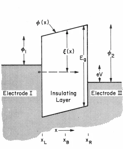
Discussions of tunneling are often based upon the transfer
. 13 14
Hamiltonian model ' . In this description an idealized tunneling structure, as schematically illustrated in Fig. II.l, is divided into three separate regions. For electrons with energies of interest, two of the regions are allowed (electrodes); the third region is unallowed
(insulator). Current flow arises when there is a net transfer of
t
4'1
e(x)
J
Eg
i~~lH~~~~HtHHHHtf
__
+
::::::::::::::::::::::::::::::::::::::::::::::::::::::::
----
e
V
llllllllllllllllllllllllllllllllll llllllllllll lllli.i.i.i.i.i.i.
: . : . : . : . : . : . : . : . : . : . : . : . : . : . : . : . : . : . : . : . : . : . : . : .
Electrode I ·:·:·:·
I nsu la ting
f=~:i:!~:~:~~=J~\i:
.·;·;·;·;·;·:·:·;·;·:·;·:·:·;·:·:·:·:·:·:·:·:·:·:·:·:·:·:
:::::::::::::::::::::::::::::::::::::::::::::::::
:HHlllllllHlllllllllllll1l lll1 lllll Ull1l l
La
ye
r
... : ·:
~ ~~~ ~~ ~ ~ ~ ~ ~
r
~ ~ ~ ~ ~ ~ ~ ~ ~ ~ ~ ~ ~ ~ ~ ~ ~ ~ ~ ~~ ~ ~ ~ ~ ~ ~~ ~ ~ ~ ~\
:
·:·:·:·:
.
:·:· :·:. :·:·:·
:·:·:·:.:. :·
..
:·:·:·:
...
:·:.:.
.
...
:
.
: : : : : : : : : : : : : : : : : : : : : : : : : : : : : : : : : : : : : : : : : : : : : : : : : : : : : : : : : : : : : : : : : :@llllllf
:::::::::::::::::::::::::::::::::::::::::::::::::::::::::::::::::::::::::::::::::::::::::::::::::::::::::::::::::::::::::::::::::::::::::::::::::::::::::::·:··
ff
tt ..
·.·:·:-::::::::ttlHHHlHHtHHtttf
ff
t
·:::::: ::::::::::::::::::: :: :: : :: ::::::::: ::::::: :=: ::::: :: : : : : :: : ::: :: :: : : : : : :: :: ::: : ::::::: :::::::::::::::: :: : : : : : : : : : : : : : : : : : : : : : : : : : : : : :; : : : : : : •
: ••••
.
~~~~~~~~~~~~~~~~~~~~~~f ~~~r~~t~~~~~~~~~~~~~~~~~~t~~~~t~=;================:====:;::========================:======:=·=·:···
·
:::::::::::::::::::::::: :::::::: :::::: ::::::: ::: :::::::: :: :
~=.:.:.:..x
..
·.·.·.·ci·.···
I
I
:
:
: :
: : : : : : : : : : : : : : : : : : : :
:
: : : : : : : : : : : : : : : : : :
:
:
::
:
:..
····=·=·=·~···~·=·=·=···
.
X
L
X
B
Fig. II. l Schematic energy band representation of an ideal metal-insula tor-metal tunneling structure in which electrode II is biased V volts with respect to electrode I. ¢1, ¢2 are metal-insulator barrier energies; ¢(X) is the
[image:49.613.129.532.111.597.2]quantum mechanical Hamiltonian
(II .2-1)
where HL is the Hamiltonian for the left electrode (see Fig. II.l),
I\
is the Hamiltonian for the right electrode and HT (transferHamiltonian) contains the interaction between the two electrodes due to the insulating region. The transfer Hamiltonian may be expressed simply in terms of basis states {la>} and {IB>}. The set {la>} is the set of single particle solutions of the Hamiltonian for the left electrode and the insulating layer which carry current toward the insulating layer. The set {IS>} is
a similar
set of functions for the right electrode. Using this basis, HT is given by the expression(II.2-2)
where MaS .= i~ JaS(~) and JaS(xB) is the matrix element of the current operator between the states a and B integrated over a plane parallel to the metal-insulator interface at some position, ~' in the
13
insulating layer That is,
where
<aj_;[(XB)jS> and S is the plane described above.
Application of Fermi's Golden Rule to compute the net rate of
transfer produced by HT gives
I(V)
211ef!
~
1Jas1
2{fL(t\,} - fR(£
13 )},
a
S
(II. 2-4)
where I(V) is the current from left to right for an applied bias
v·
'
f
1 and fR are the Fermi factors for the left and right electrode,
respectively; and E: and
a and the single particle energies of
the state a and the state
S,
respectively. In deriving equationII.2-4 it is assumed that the electrodes are adequately described by
a single particle formalism.
Evaluation of the matrix element JaB for direct tunneling
in the standard way (see, for example, references 15,16,17) yields an
expression for the current density
j(V)
=
z~1d1:::~1z
g(E,kjj )[fL(E) - fR(E)]ex+\ k(E,k\\•X)d+
(II.2-5)
where
kl!
is the parallel component of the wave vector of the electronelectronic wavefunction in the forbidden insulating region: k(E,
k\1,X)
is the attenuation constant. For single crystal insulators k may be thought of, in band structure terms, as the imaginary part of the complex wave vector18,19 within the forbidden gap. In general, k is a function of the electron energy,
E;
the parallel component of the wave vector, kll; and position in the insulator, X. The dependence on X is due to the ap-plied potential and interface potentials which change the features of the band structure of the insulator relative to the electron's energy.In Eq. II.2-5, g(E,~I) is a pre-exponential factor which results from the matching of the wavefunctions at the interfaces. Its exact theoretical form will depend on the assumed boundary conditions. Attempts at experimentally verifying the form of g(E,
kjj}
from struc-ture in the bias dependence of the tunneling current have failed15• Since k, the function of interest, is insensitive to the exact form or value of we will take it to be unity. This approximation is supported by calculations on several simple models which all yield g ::::: 1.Further simplification of Eq. II.2-5 can be realized by noting the rapid variation of the exponential factor with kl\· This allows us to use the saddle point method to obtain a useful approximation for the integral. Taking the dependence of on to be given by
we have
j (V) := (II.2-7)
Since most tunneling experiments are performed at low
temp-erature (to minimize thermionic currents) it is often a good
approxi-mation, and alw~ys theoretically handy, to take the temperature to be
zero. This approximation makes sense if the natural width of the
energy distribution of tunneling electrons is appreciably greater than
the width added by the thermal tail on the Fermi distribution in the
20 source electrode.
There remains one useful simplification of II.2-7 to be
discussed. The energy E may be related to the spatial coordinate X
such that k becomes a function of a single variable
s(X).
This newvariable ~(X) is the difference in energy between the conduction
band and the energy of an electron located at X:
s(X)
=
¢(X) - E .
(II.2-8)j(V)
=
e
2rrh
(II.2-9)
This expression, although somewhat approximate, is of adequate precision and contains the basic physics of tunneling. A quantitative interpretation of experimental data using this expression requires
¢(X)
[and hence ~(X)] be known independent of the measurement oftunneling currents.
Asstnning now the trapezoidal barrier potential21 as shown
in Fig. II.l
¢(X)
= ¢1
+ (¢2
-
¢1
- V)X/t,
and for an applied bias22 in the range -
¢
1 < V <¢
2, Eq. II.2-9 becomesv
cP. +E-VI
2~hfE expl~ =~t~V/"2 d~
2 1r.lcp
.
k(~)
1 +E
j (V) = _ _ o _ _ _ _ _ _ _ _ _ _ _
q,
2+E-V
~
+E1
d~ t
(II. 2-10)
Tilis equation is a sui.table bas:ls for 1nterprct:lng tunneling currentti Jn
structures known to have a trapezoidal barrier shape.
To interpret tunneling I-V characteristics in tenns of
k(~) (i.e., the dispersion relation for the imaginary part of the wave vector) Eq. II.2-11 must be solved for k(~} given J(V) and the other parameters in the equation. For certain values of barrier energy and applied voltage, and for certain k(~) functions, the distribution in energy of the tunneling electrons can be accurately approximated by a single sharp peak. In this case expression II.2-11 reduces to the f&miliar simple fonn12 used by Stratton et al, and the interpretation may be accomplished by simple mathematical manipulations. However, in general, Eq. II.2-12 must be solved without simplifying approximations. Thus, one is faced with solving a nonlinear integral equation of the Volterra type of the first kind. Numerical solution is unavoidable.
Equations of the type given in Eq. II.2-11 are usually solved by an adaptation of the well-known Newton's method for obtaining the roots of a system of nonlinear equations23 Basically, this technique consists of making an initial guess and then computing corrections to this guess from the integral equation. In detail, let
£{j (V),k(~)} =
exp jexp (V)
-<t>
2+E-V
exp -
(~
: :-V)~ k(~) d~
2 1 cf> +E1
bias and £ is a function of both jexp(V) and k(O. Obviously,
t
will be identically zero when a solution is attained. Let k (0 be0
the function which makes .L
=
0, that is, k(0
is the solution.0
In general, k (~) is unknown. However, some initial guess at
0
is ~G.e.. This guess k(~),
k(~)
=
k (~)-0
is related to k (~) by an equation
0
ok(~)
k (~)
0
(iI.2-13)
where ok(~) is the correction required to make k(~) equal k
(0.
0
Substituting II.2-13 into Eq. II.2-12 and expanding in a Taylor's series about k(~), we have
(II.2-14)
where o S. /ok(~) is the functional derivative of .L with respect to
k(~). Neglecting higher order terms in Eq. II.2-14, this equation gives
a value of ok(~)
ok(~)
=
-fv
ok~~)
£ -l {j (V),k(~)}
S, {j (V) ,k(t.:)}exp exp
(II.2-15)
-1
where
oS,
/ok(~) i f it exists is the inverse of the integral operator appearing in Eq. II.2-14. Existence of the inverse determines that range of j (V) which is required to specify ok(~) and k (~)exp o
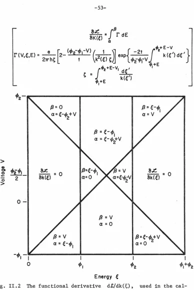
Evaluation of 8£/ok(~) may be accomplished by substituting
k(f;:)
+
ok(t.;) for k([;:) in Eq. II. 2-12 and expanding in ok(f,). Theterm Hnear in ok(O gives tS.£/cSk(O. The re:rnlt of such n CH lculn
-tion is shown in Fig. II.2 where the explicit dependence of 0£/ok(O
on V and ~ is shown. If the array in Fig. II.2 is evaluated on a
mesh in V and ~ with equal number of points in ~ and V (as is
done in the numerical solution of II.2-13), then one obtains a square
matrix. If this matrix has a deterniinant which is different from zero,
then the finite set of numerical equations which replace II.2-13 has a
unique solution. This condition determines the range of V which will
give a unique set of values of k on the mesh of ~.
0 Thus, it is
possible to test the uniqueness of the calculated solution by computing
the inverse of this matrix. While this method does not provide a
rigorous mathematical test for uniqueness, it does suffice for the
problem at hand.
. 17 24
Numerical solution proceeds in a straightforward manner ' .
Some difficulty is encountered in solving the linear Eq. II.2-13 as a
result of numerical instabilities. These difficulties may be overcome
by the use of a powerful technique recently developed by Franklin for
converting an ill-posed linear problem into a well-posed stochastic
>
CD
"'24'1_
8~~
0
8k(()
= 0
-
0 2>
o~
-4', - ,
I0
4',
13
=
v
a=O
Energy
e
I
13
=e-<Pi
I
a=V
8~
8kCe>
= O
/3=e-<P,+V
2a=O
4'2
I
4',
+4'2
[image:58.612.133.522.87.667.2]II.3 EXPERIMENTAL CONSIDERATIONS
A. Gallium Selenide
Ideally one would like to take a well characterized bulk
0
insulator, cleave it into thin section ( 100 A thick), and incorporate
these thin sections into MIM structures. Such an approach is not
usually feasible for a variety of practical reasons. There does exist,
however, a family of solids (the layer compounds) which is well suited
to this approach.
Layer compounds are distinguished by their unusual
crystal-lographic structure. Each layer (typically several atoms thick) is
strongly bonded· internally but only weakly bonded to its neighbors.
Hence, thin single crystal films can be obtained by pulling or peeling
a macro single crystal apart. This technique for fabricating
well-26
defined MIM structures was pioneered by