Generation of a High Resolution Pulse Width
Modulated Wave Using FPGA
1 Kishore Ramesh Badgujar, 2 Pankaj A. Salunkhe, 3 Tushar M. Patil
1, 2 Yadavrao Tasgaonkar College Of Engineering & Management,
University of Mumbai, Bhivpuri, Karjat, India.
3 G.H.Raisoni Institute of Engg. & Management
North Maharashtra university, Jalgaon, India.
Abstract - This paper proposes a new digital pulse width modulation (DPWM) architecture that takes advantage of the field programmable gate array’s (FPGA)advanced characteristics, especially the delay-locked loop (DLLs) present in almost every FPGA. The proposed DPWM combines a synchronous (counter based) block with an asynchronous block for increased resolution without unnecessarily increasing the clock frequency. The experimental results show an implementation in a low-cost FPGA (Xilinx Spartan-3) that uses an external 32 MHz clock for a final time resolution.
Keywords -Digital Control, Field Programmable Gate Array, Pulse Width Modulator, Signal Resolution.
1.
Introduction
Digital control of motors has obtained great research attention due to their now well-known advantages [1]–[5], such as programmability, advanced control algorithms, reduced component count, low sensitivity to external factors or aging, ease of design and prototyping, etc. However, digital control disadvantages are also ease of use well known.
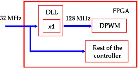
Fig. 1 Different Clock domain for the DPWM and rest of the Controller DLL Block
The key of the proposed DPWM architecture is that it takes advantage of the advanced DLL features that are available in almost every FPGA nowadays. Digital devices such as FPGAs have specific blocks that can manage clock signals: DLL or phase-locked loop (PLL). Using these DLLs or PLLs, it is pos-sible to multiply or divide the clock frequency. Many of these DLLs can also generate four phase-shifted clocks (shifted 0 ◦ ,90 ◦ , 180 ◦ , and 270
◦ ) directly (Spartan and Virtex families of Xilinx) or allow to generate phase-shifted versions of the clock(Cyclone and Stratix families of Altera, ProAsic3, Fusion, or Axcelerator families of Actel).
The two most important disadvantages are linearity in output and vibrations in the application like motor.[6]. Regarding the second factor, resolution is limited mainly by the analog-to digital converter (ADC) and the pulse-width-modulation (PWM). However, the ADC resolution is becoming a less important problem, thanks to the windowed ADC technique [3] and because the PWM resolution needs to be higher than the ADC resolution for avoiding limit cycling. Traditional digital PWMs (DPWMs) are based on counters. The advantage of these DPWMs is that they are very simple and obtain high linearity. However, their resolution cannot be very high, as the minimum time step is equal to the clock period of the counter. As the clock frequency increases the output of the PWM waveforms can be increased in accordance with the load.
to attain the frequency required for the minimizing of the vibrations in the DC motor we are trying for the same to be achieve using FPGA. However, they have lower linearity and non-monotonic behavior in some cases This paper proposes a DPWM generation. The synchronous block is counter based. However, the asynchronous block is not based on building a new delay-line structure, but using field-programmable gate array (FPGA) available delay locked loops (DLLs).
This is the main difference from previous solutions, which develop their own delay line or DLL . Almost every FPGA includes DLL blocks with phase-shifting features. Taking advantage of these resources, the proposed architecture obtains an excellent trade-off between linearity and time resolution. The proposed DPWM is, in principle, intended for FPGA implementation. An IC implementation would need the development of a DLL with phase-shifting capability, which is the most complex part of the architecture. However, as this block is already available in FPGAs, an FPGA implementation is very simple. Furthermore, the lowest cost FPGAs are suitable for the proposed DPWM, as shown in the experimental results. The paper is organized as follows. The next section describes the generation of DPWM, while Section III shows the experimental results. Finally, Section IV gives the conclusions.
2. Generation of PWM
Digital methods are the most suited form for designing PWM Generators. They are very flexible and less sensitive to environmental noise . Also they are simple to construct and can be implemented very fastly. Most of the digital techniques employ counter and comparator based circuits.
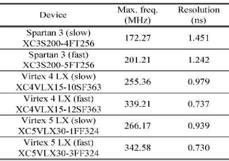
Table 1: Resolution Of The Proposed Dpwm For Different FPGA
Field Programmable Gate Array (FPGA) offers the most preferred way of designing PWM Generator for Power
Converter Applications. They are basically interconnection between different logic blocks. When design is implemented on FPGA they are designed in such a way that they can be easily modified if any need arise in future. We have to just change the interconnection between these logic blocks. This feature of Re-programming capability of FPGA makes it suitable to make your design using FPGA. Also using FPGA we can implement design within a short time. Thus FPGA is the best way of designing digital PWM Generators. Also implementation of FPGA-based digital control schemes proves less costly and hence they are economically suitable for small designs.
3. High Frequency Counter Based PWM
Generator
The synchronous block is a counter-based DPWM that uses the n − 2 most significant bits (MSBs) of the duty cycle, d[n − 1, 2], n being the total number of bits. As can be seen in Fig. 2, the synchronous block is based on a counter and comparison structure, which resembles analog PWMs based on saw-tooth signals. The functionality of this block is the following: if the duty cycle command is over the counter value, which is equivalent to a saw-tooth signal, the output is in the ON-state, and when the counter reaches duty cycle the output is turned OFF. This is a simple block , and therefore, it can work at high clock frequencies.
This architecture was proposed by E.Koutroulis , A.Dollas and K. Kalaitzakis in [9]. According to this architecture there is a high speed N-bit free running counter whose output is compared with register output; which stores desired input duty cycle( N-bit value); with the help of comparator. The comparator output is set equal to 1 when both these values are equal. This comparator output is used to set RS latch .The overflow signal from counter is used to reset RS latch. The output of RS latch gives the desired PWM output.. This overflow signal is also used to load new N-bit duty cycle in Register.
The advantage of these method is that it is used to generate High-frequency PWM output which is not possible in normal counter based approach. Fig 2.shows the corresponding block diagram of this architecture.
In the synchronous block, resolution is given by both the clock and the switching frequencies. This resolution can be obtained as:
Resolution =f clk /f sw
where f clk is the clock frequency and f sw is the switching frequency.
Fig.3 Architecture of PWM Generator
The application of PWM control in a Motor (DC/AC) is shown in Fig. The PWM control signal, VPWM in Fig., is generated from PWM generator. This VPWM is logically ANDED with rectangular pulse waveform coming from pulse generator and is fed to power switches S1 and S3.
The inverted rectangular waveform is logically ANDED with PWM waveform and is fed to power switches S2 and S4. Thus ON and OFF time of power switches are controlled by this PWM control signal to The power switch is usually of MOSFET or IGBT. The size of Inverter depends on size of these power switches.
Fig. 4 PWM Control of Inverter
The proposed DPWM has been implemented in a Spartan-3 FPGA (Xilinx), occupying only 22410 equivalent gates for a four-phases buck converter (including theDLLs). The Spartan families are the low-cost low-speed FPGAs of Xilinx; so, better time resolution results can be obtained using Virtex FPGAs. However, the objective is to show the feasibility of the method with low-cost devices. In fact, as these FPGAs can be below 2$, FPGAs could be considered for final implementation, apart from proto typing. The exact device has been aXC3S200FT256-4. The suffix -4 means a low-speed and low cost device, because even using the same family, higher speed scan also be obtained using -5 devices. The experimental results have been obtained using an external clock of 32 MHz, which is multiplied by 4 using the DLLs(called digital clock managers or DCMs in this family of FPGAs).These DCMs also generate the four phase-shifted clocks. Hence, the internal clock frequency of the DPWM is128 MHz. The final resolution of this DPWM can be calculated.
4. Experimental Results
The whole DPWM (both synchronous and asynchronous blocks) have been designed in VHDL (the same can be done in Verilog). This allows the DPWM to be implemented in any FPGA. The only part not described in VHDL is the DLL, which is given by the manufacturer as a black box. This is the only limitation for implementing this DPWM in an IC, although a similar DLL can be designed for a possible IC implementation.
Fig.5 Simulation Result of DCM based PWM
Since frequency of operation is inversely dependent upon Inverter size so we have to increase the switching frequency to reduce the Inverter size [1]. So we have to look into the frequency aspect of PWM Generator used so that we get optimized size of Inverter by proper selection of frequency of PWM wave.
The software tool used for circuit simulation was Model Sim.
In order to assure a correct VHDL description of the proposed de-sign, behavioral simulations (these simulations do not include delays) were done. However, in order to check linearity and monotonic behavior, post-place and route simulations were car-ried out. These simulations include the delays of each signal.
Using these simulations, non monotonic behavior was identified in the design of Fig. 3. Once it was changed to the design of Fig. 5, further post-place and route simulations confirmed the monotonic behavior of the corrected design. Furthermore, these simulations allowed checking how linearity was changed using different placements and synthesis options. This kind of simulation is necessary, because the delays are a key part of the design in the asynchronous block. Fig. 8 shows the HSM and LSM driving signals of the four phases of a multiphase converter also used in the experimental results (including dead times for the four phases) obtained in post-place and route simulation.
Fig.6 (a) Result 1 HSM Driving signal.
Fig.7 (b) Result 2 LSM Driving signal.
5. Conclusion
been obtained while keeping high linearity and monotonic behavior.
References
[1] High-frequency pulse width modulation emplementation using FPGA and CPLD ICs Journal of Systems Architecture 52 (2006) 332–344
[2] IEEE Trans. Power Electron. (Spec. Issue Digit. Contr. Power Electron.), vol. 18, no. 1, Jan. 2003.
[3] B. J. Patella, A. Prodic, A. Zirger, and D. Maksimovic, “High-frequency digital controller IC for dc–dc converters,” IEEE Trans. Power Electron., vol. 18, no. 1, pp. 438–446, Jan. 2003.
[4] PETERCHEV, J. XIAO, AND S. R. SANDERS,
“ARCHITECTURE AND IC IMPLEMENTATION
[5] V. Yousefzadeh and D. Maksimovic, “Sensorless optimization of dead times in dc–dc converterswith synchronous rectifiers,” IEEE Trans.Power Electron., vol. 21, no. 4, pp. 994–1002, Jul. 2006.
[6] V. Yousefzadeh, N. Wang, Z. Popovic, and D. Maksimovic, “A digitally controlled dc/dc converter for an RF power amplifier,” IEEE Trans. Power Electron., vol. 21, no. 1, pp. 164–172, Jan. 2006. [7] A. V. Peterchev and S. R. Sanders,
“Quantization resolution and limit cycling in digitally controlled PWM converters,” IEEE Trans. Power Electron., vol. 18, no.1, pp. 301–308, Jan. 2003. [8] H. Peng, A. Prodic, E. Alarcon, and D. converters,”
IEEE Trans. Power Electron., vol. 22, no. 1, pp. 208– 215, Jan. 2007.
[9] A. P. Dancy and A. P. Chandrakasan, “Ultra low power control circuits for PWM converters,” in Proc. IEEE Power Electron. Spec. Conf. (PESC), St. Louis, Missouri, Jun. 1997, vol. 1, pp.21–27.
[10] E. O’Malley and K. Rinne, “A programmable digital pulse width modulator providing versatile pulse patterns and supporting switching frequencies beyond 15 MHz,” in Proc.IEEE Appl. Power Electron. Conf. Expo (APEC), Anaheim, CA, Feb. 2004, vol. 1,pp. 53– 59.
[11] Z. Lukic, K. Wang, and A. Prodic, “High-frequency digital controller for dc– dc converters based on multi-bit sigma-delta pulse-width modulation,” in Proc. IEEE Appl. Electron. Conf. Expo (APEC),Austin, TX, Mar. 2005, vol. 1, pp. 35–40.
[12] R. F. Foley, R. C. Kavanagh, W. P. Marnane, and M. G. Egan, “An are a efficient digital pulse width modulation architecture suitable for FPGA implementation,” in Proc. IEEE Appl. Power Electron. Conf. Expo (APEC), Austin, TX, Mar. 2005, vol.3, pp. 1412–1418.
pulsewidth modulator,” IEEE Trans.Power Electron., vol. 21, no. 3, pp. 842–846, May 2006.
[13] K.Wang, N. Rahman, Z. Lukic, and A. Prodic, “All-digitalDPWM/DPFM controller for low-power dc–dc converters,” in Proc. EE Appl. PowerElectron. Conf. Expo (APEC), Dallas, TX,Mar. 2006, pp. 719–723. [14] V. Yousefzadeh, T. Takayama, and D.
Maksimovic, “Hybrid DPWM with digital delay-locked loop,” in Proc. IEEE Comput.Power Electron. Workshop (COMPEL),Troy, NY, Jul. 16–19, 2006, pp. 142–148.
[15] A. Syed, E. Ahmed, D.Maksimovic, and E. Alarcon, “Digital pulse width modulator architectures,” in Proc. IEEE Power Electron. Spec. Conf. (PESC), Aachen, Germany, Jun. 2004, vol. 6, pp. 4689–4695.
[16] Koutroulis E., Dollas A. and Kalaitzakis K., “High-frequency pulse width modulation implementation using FPGA and CPLD ICs”, Journal of Systems Architecture , Vol.52 (2006): pp. 332–344 [17] Bai Hua,Zhao Zhengming, Meng shuo,Liu Jianz
heng,Sun xiaoying, “Comparison of Three PWM strategies—SPWM,SVPWM and one cycle control” IEEE 0-7803-7885-7/03 , 2003.
[18] B. N. Mwinyiwiwa, Z.Wolanski, and B. T. Ooi,"Micro processor implemented SPWM for multiconverters with phase-shifted triangle carriers"
IEEE-IAS Annu. Meeting, NewOrleans, pp. 1542- 1549, Oct. 1997.
[19] Kay soon low “A DSP-based Single-Phase ACPower source” IEEE trans on industrial electronics vol-46,no.-5,OCT-1999.