Adjacency Exclusion Scheme Based Testing of Multiple
Cores in Four Layered Stacked SoC
1
Indira Rawat,
2M. K. Gupta,
3Virendra Singh
1Dept. of Electrical Engineering, Govt. Engineering College, Ajmer, Rajasthan, India
2Dept. of ECE, Maulana Azad National Institute of Technology, Bhopal, India
3Dept. of Electrical Engineering, Indian Institute of Technology, Bombay Mumbai, India
Abstract
Integrated Circuits have been growing in complexity with reduction in size since late 1950’s. As per Moore’s law, scale of ICs get doubled every 18 months. It is very interesting to note that the feature size has reduced from 10s of micrometer to 10s of nanometer for transistors and interconnecting wires. The ever increasing complexity in designs of VLSI circuits is the result in the reduction of size of circuits. Small sized circuits make the designed product very compact. Before introduction of these complex built circuits into market it is inevitable to ensure
the product free from any defect. This requires that the finished
product undergoes a rigorous test schedule for performing fault free during use. Testing of any product is mandatory to guarantee fault free products. However, the growing size and complexity of the circuits pose several and new testing challenges. It is quite evident that the decreased feature size increases probability of defects generation during manufacturing process. In this paper we intend to discuss test scheduling schemes of complicated 3D System on Chips (3 D SoCs) comprising of standard benchmark circuits.
Keywords
Adjacency Exclusion, 3 D SoC, Hotspot, RHDF.
I. Introduction
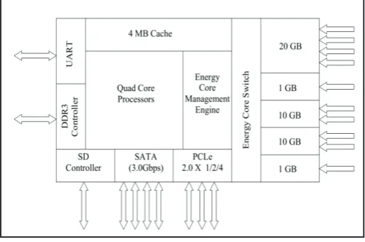
The electronic circuits have been reducing in size from SSI, MSI, LSI, VLSI and SoC. A SoC is an Integrated Circuit that integrates all components of an electronic system or gadget into a single chip thereby eliminating need of fabricating different chips on the board and then interconnecting them as per the functional requirement [1]. This scheme not only results into reduced size but also offers improved performance of the product. SoC may consist of Digital, Analog, mixed -signal or radio-frequency functions on a single chip substrate. A typical SoC invariably contains a processor, SRAM, peripheral systems and interfaces connected to the processor via SoC bus, microcontrollers etc. A typical SoC
is shown in fig. 1.
Fig. 1: A Typical SoC Circuit
These SoCs are commonly used in new electronic gadgets like mobiles, digital camera etc. The SoCs offer multiple advantages like, reduced power consumption, increased reliability of the product, smaller size and space, reduced product cost, makes product faster in operation. However these SoCs are also having disadvantages attached to them like extremely high designing cost, complex component testing long time in prototyping etc.
A. 3-D SoC
These SoCs have been further miniaturized by way of introduction of 3D-SoC where multiple SoCs are stacked upon each other.
These 3 D SoCs offer many benefits like further reductions in die size and power consumption, offers significant advantages for
reusing the same fab lines and design tools, permits heterogeneous integration, by way of processing multiple layers simultaneously; it offers enormous cost improvement, logic redundancy permits x100 integration at better yields and offers modular platforms. Fig.
2 shows a typical 3-D SoC which indicates the design flexibility
aspect of 3 D SoC.
These complexed circuits need to be tested rigorously for fault free performance. Testing has great impact on cost as the cost to detect faulty IC by an order of magnitude of 10 as we move from Device to PCB to System to Field operations; testing is mandatory at all levels. Testing during manufacturing improves yield. Field operation testing ensures fault free system operations.
II. Background
In the field of testing a lot of work has been done. The SoC testing Process may be categorized as Verification Testing, Manufacturing Testing, Reliability Testing, Acceptance Testing. Here Verification Testing or Design Verification verifies correctness of design and
test procedure whereas manufacturing testing ensures that the parts are correctly manufactured. Reliability Testing ensures reliability of the product and is conducted by applying higher power supply, exhaustive test time application for monitoring temperature rise of the chip. Acceptance test is done at customer premises before putting system in use. In this paper, author cover reliability test of SoCs. The main concern in reliability testing of SoCs is proper application of test vector for thorough testing of SoC [2]. The challenges faced in SoC are many out of which power generated due to fast switching activity is 3-10 times the functional power. This increases the overall chip temperature and creates spots of localised heating called hotspots [3]. These hotspots may damage the chip permanently and therefore need high cooling costs. This heat has to be removed from the surface of the microprocessor die at the rate of its generation by way of cooling methods. In [4-5] remarkable work has been reported for this. during test is a main issue. C.Yao et. al. [6] have addressed issues of testing of circuits. They have suggested that parallel testing of cores helps in test time reduction. Other noteworthy work done under this head comprises [4] the mixed integer linear programming by K. Chakraborty in ITC 2001. In VTS’03, scheduling based on simulated annealing was presented by W. Zou, Reddy and others [7] Heuristic algorithm (k-tuples) and Multi-TAM problems by S. Koranne and V. Iyengar in IEEE TCAD 2002 [8]. IEEE P 1500 standard has been reported by F. Dasilva , Y. Zorian et. al in [9]. The origins of 3D dates back to 80’s when James Early of Bell laboratories in [10] discussed 3D stacking of electronics and predicted that heat removal from such an integration would be the main concern. In [11-13] the original concerns of test scheduling were dealt suitably. Test resource
conflict was a major consideration at that time. W-D Tseng in 2006
have proposed Power constrained Test Scheduling [14] where they have presented a method to integrate the management of power consumption to augment the parallelism of the testing activities for reduction of total test time. In [15] Wu. et. al. in 2008 presented an optimization technique for test time minimization for 3 D SoCs. In 2009, Jiang et al [16] gave 3D test access mechanisms by taking pre-bond test times into account to optimize total test times.
III. Earlier Work Done by Authors
In [17] authors worked on some benchmark circuits and proposed a methodology to test cores of SoC wherein a particular core is selected for testing, after testing, the Heat Flow as per Fourier Law of Heat Conduction to adjacent cores were considered and the temperature rise was monitored. In following tests, the core with the lowest temperature was selected and the process of testing was repeated. In this fashion all cores were tested one by one. This scheme was compared with the scheme of testing cores sequentially in the stack for temperature performance and the proposed scheme’s result were found to be superior which was further authenticated during validation. However, this scheme of
testing of cores one by one was further improved for concurrent testing of cores of stacked SoCs. After further work, in [18], authors therefore proposed a test scheduling methodology for parallel testing of cores of SoCs comprising of standard benchmark circuits [19]. The benchmark circuits used were d695 (10 cores), d281 (8 cores), f2126 (4 cores) and 2f 2126 (8 cores). Authors have suggested a methodology where in all cores were arranged in an array of decreasing order of their RHDF (Relative Heat Dissipation Factor) value. This RHDF value was calculated based on the placement of cores in the stack and the P_Trace value to be applied to the cores which also contribute to the heat accumulated in cores. This sorted array gives us the cores arranged in a fashion where the core which has highest heat accumulated coupled with the factor of slowest heat dissipation rate gets placed at the top.
Our methodology was centered at picking up these cores first for testing so as to give them sufficient time to cool down during
complete test of SoC and also give these cores the advantage of its initial cool neighbors to enable it to dispense away the generated heat. During generating test schedules, care was taken to avoid picking up of adjacent cores in the stack i.e. Adjacency Exclusion Approach in selecting cores so as to avoid formation of hotspots by way of localized rise of temperature. The generated test schedules for 2, 3 and 4 layers of d695 and d281 for 2 layers, d695, d281 and f2126 for 3 layers and d695, d281, f2126 and 2f2126 for 4 layered SoCs were listed in [18]. These test schedules were implemented on Hotspot, which is a validated tool for test simulation and the results were obtained. The results of testing were compared with the conventional sequential testing scheme of layers of SoC wherein layers of SoC are tested one by one, and the results are compared to show the superiority of proposed algorithm over sequential scheme.
In this paper, authors propose to extend this methodology to test 4 layered stacked SoC comprising of combination of some other benchmark circuits and then studying the behavior in terms of temperature rise and test time taken; comparing it with the results of sequential testing and verifying the superiority of the methodology being worked upon by authors.
IV. Problem Formulation
In this paper we are considering a stacked 3 D SoC of 4 layers i.e. a 3 D stacked SoC of 4 nos. of benchmark circuits with all circuits arranged in 4 layers. If i represents the number of layer with i varying from 1 to 4 then xi represents the total number of cores in ith layer. Total cores in the SoC are indicated by x1 + x2 + x3 + x4. These total cores are to be arranged in parallel test scheduling so that maximum possible number of cores are selected in any schedule for testing. Moreover the cores so selected in a particular schedule should follow Adjacency Exclusion Scheme i.e. the cores so selected in any schedule are non adjacent to each other vertically as well as horizontally. Firstly, all cores are arranged in an array for convenience of forming schedules. The cores are selected from this array which is the sorted array based on the RHDF values of the cores. In our paper we are picking up SoCs built up by using g1023 (14 cores), h953 (8 cores), d281(8 cores) and 2f2126 (8 cores). The 4 layered stacked structure has g1023 closest to heat sink followed by 2f2126 then h953 and
finally d281 which is farthest from the Heat Sink. The benchmark
Fig. 3: A g1023 Benchmark Circuit
Fig. 4: A h953 Benchmark Circuit
Fig. 5: 2f2126 Benchmark Circuit
Fig. 6: A d281 Benchmark Circuit
Fig. 7: The 4 Layered Stacked SoC
V. Test Scheduling Algorithm
The Algorithm proposed by authors in [18] is being presented here for understanding the problem.
A. The Algorithm Description
Let there be N No. of Floorplans with x
1. i cores in ith floorplan,
Total cores = x1 + x2 +...xi+...xn.
Input all the parameters of the cores like cordinates, P_Trace 2.
values of the cores.
Calculate HHDF, VHDF and RHDF of all cores on the basis 3.
of their placement and P_Trace values.
Sort all cores in terms of RHDF values in descending order 4.
of their RHDF value and store them for further testing Select cores which are not tested yet from this sorted list for 5.
preparing Test Schedule by Adjacency Exclusion Principle. Display Test Schedule no. & cores in the Schedule 6.
generated.
Test all cores of this Test Schedule on HotSpot and record the 7.
Display Temperature of all cores after testing Schedules on 8.
Hotspot.
Repeat the procedure till all cores are tested. 9.
Display total time of the testing, Max Temp during the testing, 10.
mean temperature of cores and of total chip.
B. Implementation of Algorithm
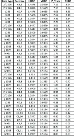
Table 1 shows HHDF, VHDF, P_Trace and RHDF of cores in a 4 layered stacked SoC.
Table 1: Details of Cores in 4 Layered Stack
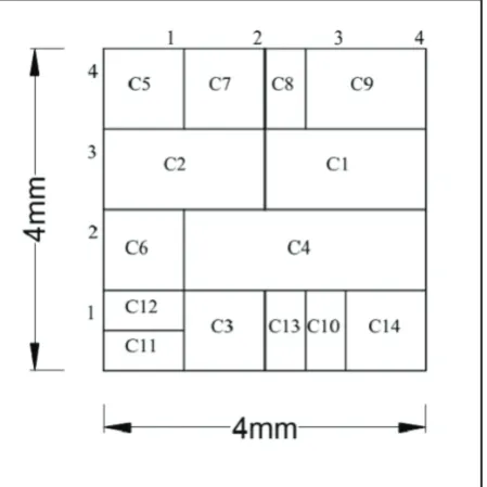
While implementing on Hotspot, the layer which is farthest from Heat Sink gets numbered 0 and then the Thermal Interface Material (TIM) which is interface between two active layers gets numbered 1. Similarly all active layers get numbered even with highest even no. allotted to the layer closest to Heat Sink and all TIMs get odd numbering after test on Hotspot. The sorted array of cores on the basis of their RHDF values after applying this algorithm is shown in Table 2.
Table 2: Sorted Cores of 4 Layered Stack
After the array gets sorted, test schedules are generated on the basis of Adjacency Exclusion Scheme. The core with a High RHDF means it gets heated the most and its dissipation heat capacity is slowest, i.e. the worst performing cores in terms of heat dispensing should be taken on priority during testing. Our
scheduling methodology picks up such cores first for testing to
take advantage of all initially cooled cores and to give these cores maximum time to cool down during course of testing.
VI. Generation of Test Schedules
The sorted cores on the basis of their RHDF values are displayed in Table 2 for 4 layers stacked SoC. From these sorted cores the algorithm of test scheduling generates test schedules for implementing on Hotspot. The schedules so generated are displayed in Table 3 for our 4 layered stack. Figure 8 depicts the cores of individual layers selected on the basis of Adjacency Exclusion Approach for testing. From Figure 8 it can be easily
figured that that no two cores in any test schedule are adjacent to
Table 3: Test Schedules for 4 Layered Stack Sch. Selected Cores (Layer – Core No)
Sch 1 0-2, 0-7, 0-8; 2-2; 4-2, 4-5, 4-7; 6-6, 6-7, 6-11, 6-13: Sch 2 0-3, 0-5, 0-6; 2-8; 4-1, 4-3, 4-6; 6-3, 6-5, 6-9, 6-14: Sch 3 0-1, 0-4; 2-1, 2-3; 4-8; 6-2, 6-8, 6-10, 6-12: Sch 4 2-5, 2-6; 4-4; 6-4:
Sch 5 2-4, 2-7; 6-1:
Fig. 8: 4 Layers Test Schedules Generation
The core which has the highest value of RHDF is selected first, here core C4,2 is the core selected first but the second highest
RHDF core C 4,6 is adjacent to it, this core is excluded from Sch 1 and the next core C 0,7 is selected which is non adjacent to earlier selected core. In Table 4 we are showing the P_Trace values of each core applied during implementing on Hotspot. P_Trace is the 1:400 ratio of clock cycles applied at 1.2 GHz. In Hotspot we are using clock cycle of 3 GHz so this ratio is 1:1000. In some schedules some blue shaded P_Trace are present which indicate the residual P_Trace after the previous test. The colour of each core indicates the test schedule in which that core falls for testing.
Table 4: P_Trace Values Applied In Schedules
VII. Results and Conclusion
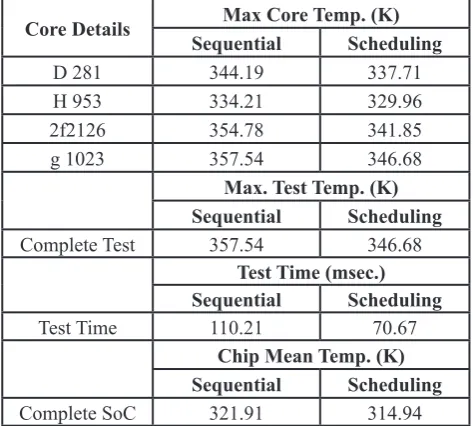
The Test Schedules were applied on Hotspot tool and the results in the form of temperature of the cores were recorded. The highest temperature after every test were recorded along with the max. Temp. of the complete test. The mean temp. of the whole chip was also calculated. These parameters were also measured for sequential testing of cores in which the cores were tested layer wise. The parameters obtained after sequential testing are compared with that of scheduling as per the proposed algorithm and the results are tabulated below in Table 5.
From this table it is quite explicit that the results after Test Scheduling are better as compared to the results obtained after testing of cores sequentially. Authors have implemented this test scheduling approach on various combinations of benchmark circuits and layers and the results of this test scheduling approach has always been found to be better than the results of sequential
testing approach. Authors are working in this field and wish to
extend this scheme after implementing TSVs in the stacked circuits which will help in further reduction of the highest temperature reached during testing.
Table 5: Tabulated Results of 4 Layered Stack
Core Details Max Core Temp. (K)
Sequential Scheduling
D 281 344.19 337.71
H 953 334.21 329.96
2f2126 354.78 341.85
g 1023 357.54 346.68
Max. Test Temp. (K)
Sequential Scheduling
Complete Test 357.54 346.68
Test Time (msec.)
Sequential Scheduling
Test Time 110.21 70.67
Chip Mean Temp. (K)
Sequential Scheduling
References
[1] Erik J. Marinissen, Yervant Zorian,“Challenges in Testing Core-Based System ICs”, IEEE Communication Magazine, June 1999, pp. 104-109.
[2] P.K. Nag, A. Gattiker, S. Wei, R. D. Blanton, W. Maly, “Modelling the Economics of Testing - A DFT Prespective”, IEEE Design and Test of Computers, 10 (I): January 2002, pp. 29-41.
[3] B. Vermeulen, C. Hora, B. Kruseman, E. J. Marinissen, R. Rijsinje, “Trends in Testing Integrated Circuits”, IEEE Test Conference, 2004. Proceedings. ITC 2004. IEEE, 26-28 Oct 2004, pp. 688-697.
[4] Huang, W., Ghosh, S., Velusamy, S., Sankaranarayanan, K., Skadron, K., Stan, M. R.,“Hotspot: A Compact Thermal Modeling Methodology for Early-Stage VLSI Design”, In IEEE Transactions on VeryLarge Scale Integration (VLSI) Systems, 14(5), pp. 501–513, 2000.
[5] Pedram, M., Nazarian, S.,“Thermal Modeling, Analysis and Management in VLSI circuits; Principles and Methods”, In Proc. IEEE, Vol. 94, Issue 8, 2006, pp. 1487-1501.
[6] Yao, C., Saluja, K. K., Ramanathan,“Test Scheduling for Circuits in Micron to Deep Submicron Technologies”, In International Conference on VLSI Design, 2011.
[7] Zou,W., Reddy, S.M. ,. Pombenz, I., Huang, Y.,“SoC Test Scheduling using Simulated Annealing”, In Proc. IEEE VLSI Test symposium, 2003, pp. 325-330.
[8] Koranne, S., V. Iyengar,V.,"On the use of k-tuples for SoC Test Schedule representation”, In Proc. ITC 2002 pp. 539-548.
[9] Dasilva, F., Zorian Y. et.al.,"Overview of IEEE P1500 Standard”, In Proc. IEEE International Test Conference, 2003, pp. 988-997.
[10] Early, J.,"Speed, Power and Component Density in Multielement High Speed Logic System”, In Proc. IEEE International Solid State Circuits Conf. pp. 78-79.
[11] C.R. Kime, K.K. Saluja,“Test scheduling in testable VLSI circuits”, Intl. Symposium on Fault Tolerant Computers, 1982, pp. 406–412.
[12] H. Krawczyk, M. Kubale,“An Approximation Algorithm for Diagnostic Test scheduling in Multicomputer Systems,” IEEE Trans. on Computers, C-34(9): 1985, pp. 869–872. [13] M.S. Abadir, M.A. Breuer,“Constructing optimal test
schedules for VLSI circuits having built-in test hardware”, Intl. Symposium on Fault Tolerant Computers, 1985, pp. 165–171.
[14] W. D. Tseng,“Power –Oriented test Scheduling for SoCs,” International Journal of Computer Science and Network Security, Vol. 6, No. 11, November 2006.
[15] X. Wu et.al,“ Test- Access Mechanism Optimization for Core-based Three Dimensional SoCs”, In Proc ICCD, 2008, pp. 212-218.
[16] Jiang et.al,“Test Architecture Design and Optimization for Three Dimensional SoCs,” In Proc. DATE, 2009, pp. 220-225.
[17] Indira Rawat, M. K. Gupta, Virendra Singh,"Test Scheduling of Stacked 3 D SoCs with Thermal Aware Considerations”, IJCA, Vol. 120, No. 7, June 2015, pp. 28-35.
[18] Indira Rawat, M. K. Gupta, Virendra Singh,“Parallel Test Scheduling of 3 D Stacked SoCs with Temperature and Time Constraints”, IOSR-JVSP, Vol 5, Issue 4, Ver. 2, Jul-Aug 2015, pp. 1-13.
[19] Erik J. Marinisen, V. Iyenger, K. Chakrabarty,“A set of benchmarks for modular Testing of SoCs”, ITC, 2002.
Indira Rawat is a Ph.D scholar at Maulana Azad National Institute of Technology Bhopal, India. She is also a faculty at Govt. Engineering College, Ajmer. Her research interest includes VLSI Testing, Design for Testability and Control Systems applications.
Dr. M.K. Gupta is a Professor at Maulana Azad National Institute of Technology, (MANIT), Bhopal, India. He has done B.E. (Electronics), M-Tech (Electronics),PhD in Electronics Engineering. His research interests are
in the field of VLSI, Integrated Circuit,
Microprocessor, Control System and Image Processing. He has guided several
Ph.D students in these fields. He has a
number of national and international publications to his credit.
Dr. Virendra Singh is an Associate Professor at Indian Institute of Technology, (IIT), Bombay, Mumbai. He did his Ph.D from Nara Institute of Technology, Japan. His research interests are Computer Architecture, Processor architecture
& micro-architecture, Reconfigurable
computing, Adaptive computing/ architectures, Compiler support for modern architectures, Fault-tolerant computing, Robust design and architectures, Self-healing system design, VLSI testing and design for testability, SoC/NoC design and test. He has a number of international publications to his credit. He has guided many Ph.D