DESIGN OF MESSAGE DETECTOR AND ERROR
CORRECTOR USING FAULT SECURE ENCODER
TECHNIQUE FOR NANOMETRIC RELEVANCES
Jada Indirapriyadarsini
1, A. Syam Kumar
2,
L. Srinivas Reddy
3 1M. Tech Scholar (DECS), Nalanda Institute of Engg and Tech.(NIET),
Siddharth Nagar, Guntur, A.P, (India)
2
Asst. Professor (ECE), Nalanda Institute of Engg and Tech. (NIET),
Siddharth Nagar, , Guntur, A.P, (India)
3
Assistant. Professor (ECE), Nalanda Institute of Engg and Tech. (NIET),
Siddharth Nagar, A.P. (India)
ABSTRACT
In this paper we are presenting a novel method of error correcting codes, fault secure Encoder and Decoder for
reducing error rate. Regular memory systems and its supporting circuitry may also suffered from the soft errors.
Every memory system is having with detector and corrector. In order to reduce the soft errors in memory
system, we are developing a fault secure corrector and detector mechanism. These are based on the new method
of error correcting code called Euclidean geometry low density parity-check. This code having capability to
tolerate bit errors and transient errors. This memory fault secure detector and corrector is designed with
Verilog HDL. This description is synthesised in Xilinx ISE 13.2i. The usage of EG-LDPC yields better reliability
and lower area.
Keywords: Encoder, Decoder, EGLDPC, Soft Errors
I.
INTRODUCTION
Introduction of Nano technology yields the devices smaller, faster and require less energy which makes circuits
to operates more powerful. Nanoscale devices may not reliable because of their compactness. Faults occurring at the Nano scale devices may also have higher in quantity with compared to the today’s devices. We observed that
combinational logic families are also suffer from the faults in addition to the memory devices. We have to
design a method to protect the memory and its associated combinational circuitry. The method is having fault
secure detector and corrector with EG-LDPC. To implement this design we should develop a new type of error
correcting code which makes the design simple to fault tolerant detector. This error correcting code has exact
redundancy to identify faults in both memory locations as well in the combinational circuits connected with it.
This kind of codes are called as fault secure detector capable Error correcting codes. The fault secure detector
ECC parity-check-matrix has particular structure, that detector circuit generates parity-check matrix is a fault
secure.
The FSD is used to design the fault secure encoder and corrector. This can be used identify the faults in either of
the circuits and also repeat the function to generate exact output. With the help of corrector we correct the faults
make the design fully fault tolerant. Following section has analysis of the following
1). Fault secure detector ECC is define d mathematically and it don’t need any more redundancies.
II. RELATED BACKGROUND
Conventionally, Memories are frequently suffers from the transient faults but its associated circuitry is not
suffers from the faults. So we mainly focus on preserving memory from the faults. When the devices are scaling
down the combinational circuitry is also suffers from the transient faults or defects. The small scale devices are
not reliable properly. Implementing of the devices with scaled design is beneficial since scaled devices yields
better area, speed and in power but it has reliability problems. We should try to implement devices with scaled
design and flexibility. Conventional designs to protect encoder and decoder circuitry which require some additional logic to implement it. Here we are proposing a method which doesn’t require any extra redundant
logic to preserve encoder and decoder circuitry. In the existing design of secure encoder having concurrent
parity detection scheme. This scheme finds the parity of the incoming bits parallel as encoder process the input
bits and this parity is compared with the parity check matrix output of the encoder. This scheme will find only
single bit error. The proposed design finds multi bit errors in the corrector and encoder units.
In the proposed fault secure encoder and corrector having parity check matrix which will identify the parity of
the incoming bits into the Encoder and corrector.
III. SYSTEM OVERVIEW
Fault secure memory design that can tolerate errors in any part of its associated circuit including corrector,
detector and memory/storage bank. Assume E be the maximum number of error bits in that the code can correct,
D be the maximum number of error bits it can detect. Let em, ee and ec are the number of errors in memory,
encoder and corrector respectively. Ede and edc are the number of errors in
Two separate detector observing encoder and decoder. Traditional designs will correct the errors as long as ρ
e
m < E,e
e +e
de < D ande
m +e
c+e
dc < DThis design can be implemented when it follows below criteria
1). When encoder or corrector circuits having single error it will corrupt the total code word
2). Fault secure detector circuit will detect any type of the errors in the received code word in the detector circuit.
This will verify the functionality of each device.
We can satisfy the first axiom by avoiding logic sharing between the producing code word in the corrector and
encoder. We proposed a design of fault secure detector shown in the following diagram. Its operation as the
bits. The encoder will encode the word. That code word will be stored in the memory. During the memory
access the code word read by the corrector. During when the code word is storing in memory suffer from errors.
The code word is read by the corrector circuit which will detect the errors and correct it according the encoding
format. The fault secure detector will coordinate the operations of the correction circuit.
Data will stay in the memory for a long time of memory access cycle. During this operation the bits in the
memory are susceptible for transient faults. For every bit is having the fault becoming all the bits accumulate
with transient faults. These fault accumulation can be cancel out by process called scrubbing. The scrubbing is a
process of periodically reading the code word from the memory and correct the error bit, again store it back into
memory. Perform this operation until it will complete for all words in memory. For this to happen we should
stop normal memory access and perform scrubbing on memory. We will discuss about each and every block of
fault secure detector in forthcoming sections.
IV. FAULT SECURE ENCODER WITH ECC
We are describing fault secure encoder with the ECC.
Background for ECC:
Let d= (d0, d1…………dnk-1) be the information vector of k-bit. This k-bit information is encoded as n bit
code word w= (w0, w1 …wn-1). Encoding information will perform vector multiplications
w = d.G
G is the generator matrix. The parity check matrix will identify the validity of the encoded vector. The order of
the matrix is (n-k)*n, elements this matrix is belongs to binary number system. The detection of error can be
described as multiplication of two vectors
S=d.HT
It is (n-k) order vector called as syndrome. If the code word is valid its syndrome will be zero. If the syndrome is
non zero the code word will be invalid. A code word said to be systematic if only if it’s having information of k
bits and (n-k) parity bits appended to it. We can define generator matrix of systematic code as following
G = [I: X]
Where I is k*k matrix identity matrix and X is k*n-k matrix. If we use systematic codes we don’t require
decoder circuit for specify the information bits. We can easily identify information from first k bits of code word.
Any code said to be cyclic if all shifts of that respective code word is still valid. If any code is cyclic if its
generator and parity check matrix rows are cyclic shifts of their first rows.
We can define minimum distance of the any ECC as the minimum number of code bits that are different
between any two code words. EC will detect the errors up to l-1 and it can correct up to maximum of l/2. An
error correcting code can be represented as (n,k,l), which represents code word length, information length and
minimum distance respectively.
V. EUCLIDEAN GEOMETRY CODES
These are often called as EG-LDPC. Since this code is low density parity check code. A low density parity
check code which is having limited number of ones in in row and columns of matrix. The limited number of
ones offers limited complexity for its detectors. We represent Euclidean geometry as EG is having following
1. Every line consist of ρ points
2. Any two points are connected by exactly one line
3. Every point is inserted by γ lines
4. Two lines intersect in exactly one point or they do not intersect
Let H be a J*n binary matrix. This matrix rows and columns are belongs to the points and lines in the Euclidean
geometry. In this matrix element is represented by hij =1, when ith line contains jth point only else hij = 0. The
matrix rows represents points on a specific line of EG with weight of ρ. Matrix columns represents that lines
that intersect at specific point with weight γ. We can call rows of H matrix as incident vectors and columns as
intersect vectors. We can say H is an intersect matrix with the lines in EG over points in EG. We illustrate some
example of EGLDPC code to understand the properties of it. The I2-D EGLDPC properties are as follows
Information bits=22t-3t
Length n=22t-1
Minimum distance l min 2t+1
Dimension of parity check matrix n*n
Row weight of parity check matrix is 2t
Column weight of parity check matrix is 2t
There is no rule that rows of H matrix must be linearly independent and they no need to represent rank of H
matrix. The rank is simply n-k which makes the code word as linear.
5.1 FSD-ECC for EGLDPC
Here we will prove that EG-LDPC code having FSD- ECC property. Let C be an EG-LDPC code with distance
d and weight γ. We have to show that nay error vector of weight 0<e<d-1 corrupting the received vector has
syndrome of weight d-e. Any particular bit in the syndrome is one when only its corresponding parity check sum
has odd number of errors in it.
In this geometry each error represents a point an each bit in syndrome denotes a line in this geometry. As a
result we are interested in finding lower bound that number of lines that move through an odd number of errors.
We can kept lower limit that number of lines that move through exactly one of the error. We defined that γ are
the lines that pass through each point. e is the error will affect the γe lines. Any point in geometry will connect
single line. Coming to the error points there are nearly 2(e2) lines between the pair of error points. The number
of lines that are passing through the accurately one error point, this gives us lower bound on the syndrome
vector weight is at least γe-2(e2)
We can conclude that weight of a syndrome vector of a code word with e errors is at least d-e when e >0.
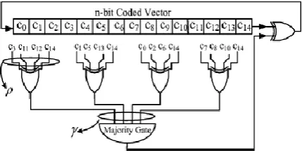
VI. DESIGN OF FAULT SECURE DETECTOR
Here we presenting the detailed description about each every module involved in fault secure detector. We also
Fig No 6.1. Fault-Secure Detector For (15,7,5) EG-LDPC Code. All The Gates Except The Final OR Gate
Are Implemented With Fault-Prone Nanoscale Circuitry. The Last OR Gate Is Implemented With More
Reliable Lithography Technique
6.1 Nano Memory Architecture
Nano memory is used to implement the memory and Nano PLA is used for implementing memory supporting
circuitry. Nanowire crossbars are used to implement Nano memory and Nano PLA. Nano memory architecture
achieve bit density of 1011 b/cm2 area. We also include lithographic scale address wire and wires. This
architecture use nanowires to implement nano memory and lithographic scale wires to implement control and
address lines. When there exists a crossing of two Nano wires it forms crossbar, at this cross bar we store the
data. In order to store a code word at the junction we should select unique row and column wire to access the
junction. The selection of proper rows and columns done by the row and column decoders. This decoders are
also implemented by the nanowires. Basically lithographic interface is used for the access between the memory
and its associated circuitry. This circuitry and memory are designed by nano wires, so interface can also
designed by the nanowires i.e. Nano wire based de multiplexer is used here.
6.2 Fault Secure Detector
The main theme of the detector operation is to calculate the syndrome. Syndrome which can be calculated from
the multiplication of the vectors encoded vector Wand parity check matrix H
s = w.HT
Every bit in the syndrome vector is result of product of w with the row in the parity check matrix. The result is
a linear binary sum on digits of code word, where the respective digit in the matrix row is 1. The binary sum
will be implemented with the XOR gate. The ρ is row weight of parity check matrix . We need a OR gate with ρ
number of inputs to produce one bit syndrome. For over all detector we need n(ρ-1) two input XOR gates. In
order to avoid logic sharing us should implement each bit in syndrome with a separate XOR gate. Any of the bit
in the syndrome is non zero then there must be an error. To find that error syndrome all bits are Logical ORed
together. The output of the OR gate detects the error signal. We should implement or gate with substrate when
there must be a point failure. OR gate size is less with compared to the XOR gate when they are implemented by
6.3 Encoder
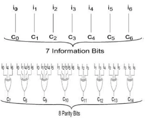
Fig No 6.2. Structure Of An Encoder Circuit For The (15, 7, 5) EG-LDPC Code; I0 To 16 Are 7-Bit
Information Vector. Each Of The XOR Gates Generate One Parity Bit Of The Encoded Vector. The
Code Word Consists Of Seven Information Bits Followed By Eight Parity Bits
Code word having n bits. The k-bit information vector I is encoded by the code word of n bits. This the
information vector generated with generator matrix G. we c say that EG-LDPC codes are not systematic codes.
We should not decode the information from the encoded vector since it adds delay to detection process. This
codes are cyclic codes. We make conversion from cyclic to systematic codes.
The encoded vector consist of information bits followed by the parity bits. Where every parity bit is product of
information vector with column of matrix X. The generator G is given as
G = [I: X]
Encoder circuit is used to compute the parity bits of EG-LDPC codes. From the figure we describe that bits
from i0………i6 are copied directly into encoded code word from c0…c6. Remaining encoded code words, and
parity bits are the linear sums of the information bits. The building block we consider is two input XOR gate, for
complete encoder structure we require 22 two input XOR gates. Encoder structure is very similar to the detector
but is having varying input XOR gates.
6.4 Corrector
The popular method of error correcting code is one step majority logic correction. There are very limited ECC
which are corrected by the majority logic corrector. We will see about one step majority logic corrector. One
step majority logic corrector: this is a method which is used to identify the correctness of the each bit from the
received code word. This is different than the normal general message passing error correction method which
results in repetetiions or loops, error and trails, which inturns increase the processing time. In this method we
avoid iteration and makes latency to be small. This can be excuted in two manners either serial or parallel to
provide compactness or minimize latency depend on the context. It’s having two phases a). Generating specific
set linear sum based on the input received code word. b). find the majority value for each linear sum to identify
the correctness of the sum bit. If the majority value is one. The bit gets inverted else unchanged the bit.
Received encoded bit linear sums are computed by making inner products of the received encoded vector with
Fig No.6.3 Serial One-Step Majority Logic Corrector Structure To Correct Last Bit (Bit14th) Of 15-Bit
(15,7,5) EG-LDPC Code.
The γ parity check sum is used to one step majority logic correction. The error correction method is described as
follows
1).The γ parity check matrix is generated from the received encoded vector multiplied with appropriate rows of
parity check matrix to generate parity check sum.
2). the γ check bits are fed to the majority gate to detect the correctness of the sum bit. The bit c get inverted if
that bit respective value of majority gate should be one.
Consider the implementation of the serial one step majority logic corrector. This circuit generates γ check sums
computed from the row of the parity check matrix with the row density ρ. It uses γ XOR gates. Then majority
value is computed from the parity check sums. Every XOR gate that computes check sum of ρ inputs. The XOR
gate corrects the single bit Cn-1 depend upon the output of majority logic gate. Then corrected bit will be shifted
cyclically. The cn-2 replaces its preceding bit Cn-1. Then the correction can be made similar to cn-1. If majority
gate has 3 inputs a, b ,c is computed with 3 product terms and 3 input or terms
II). Majority Circuit Implementation
We design majority logic circuit using sorting networks. The majority gates has the compact implementation
due to sorting networks. For n number of digits majority is the median for the given numbers.
1. Divide the given binary numbers into two halves
2. Sort the every half
3. The median is 1 when j =1, 2…….l/2 and (l/2+1-j) the element of other half are both one.
Sorting circuits will arrange the information in specified format. N-input network will sort n numbers. We have
shown here 4 bit sorting network implemented using 2 bit sorter block. The vertical line represents comparator
which compares the magnitude of any two bits and keep large value on top, low value at the below. The 4 bit
sorting network contains five compactor blocks. Each comparator having two inputs. To check condition of
median we implement n/2 two input AND gates followed by the n/2 input or gate.
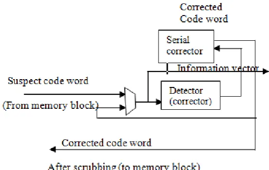
III). Serial Corrector
Serial corrector will correct the received encoded word of cyclic code. It will correct each bit serially shifts it
cyclically and replace its position with its next bit. The shifted bits are fed to the XOR gate. The corrector takes
n cycles to correct an n bit length code word. If the code word is error free then rarely we use corrector. The
corrector latency is not having great impact on the memory read access time. Those code words which are stored
in the memory are retrieved from the memory and placed in the detector. The detector circuit finds any error it
will sent to the corrector circuit. Corrector circuit will takes some iteration to find its error so the latency is
detector plus n iterations.
Fig No 6.6.Partial System Overview With Serial Corrector. Here Only The Corrector And Its Detector
Are Shown; These Blocks Connect To The Memory Block And The Rest Of The System
IV). Parallel Corrector
If the fault rate is high in the encoded code words serial corrector need excessive delay. This delay will affect
the memory access. So we require a parallel corrector which having n copies single bit corrector connected in
parallel. In every cycle atleast one code word will be corrected. The error correction is monitored by the detector
circuit. If any erroneous correction has occurred then detector circuit will give a signal to corrector. To recorrect
the word. Fault free memory word comes from the detector and corrector circuit not from the memory. Since
detection process happens rarely. All our basic elements are two input gates number of ρ input parity check sum requires γ* (ρ-1) 2 input XOR gates.
6.5 Banked Memory
Here the large memory is divided into smaller groups called memory banks. The reason for dividing the
memory is to trade-off between the memory density and access speed.
Fig.No 6.7 Banked Memory Organization, With Single Global Corrector.
The large number of smaller memory banks require large area. The large memory bank require longer wires to
access its rows and columns. Which has the disadvantage of breaking and bridging faults. The long wire has
large capacitance which is factor of delay. This capacitance will reduce the speed of access. Organisation of
conventional memory banks are similar to the Nano memory the difference is at scale, size of the memory bit
and its associated circuitry.
Fig.No 6.8 Banked Memory Organization With Cluster Size 2
The memory scrubbing can be done frequently to avoid faults in the memory banks. The error rate is directly
proportional to the scrubbing time. If the errors are more in the system it require longer scrubbing time.
to make scrubbing over all the memory banks in parallel. For parallel operation we require separate detector
and corrector for the each memory bank. Which in turn increases the overhead. To reduce this we form clusters
of banked memories. For each cluster having its own detector and corrector circuit. This will increases the
correcting rate.
VII. SIMULATION RESULTS
Here we are designing the fault secure detector with Verilog HDL. This design is simulated in Xilinx ISE13.2 i.
The synthesis reports proved that it is efficient.
VIII. CONCLUSION
In this paper we presented a fault secure detector with EG-LDPC codes. The fault secure detector itself contains
an encoder and decoder for memory. For the identifying and rectifying fault easily done by the EG-LDPC codes.
This secure encoder and decoder is designed in Verilog Hardware Description Language. This design is
synthesised in Xilinx ISE 13.2 I. This synthesis results proves that it is having better fault reduction mechanism
with compared conventional memory systems. It also proves that EG-LDPC codes are better for detecting and
correcting the faults in memory.
IX. REFERENCES
[1] IEEE transactions on very large scale integration (VLSI) “Fault Secure Encoder and Decoder for
NanoMemory Applications” Helia Naeimi and André DeHon, SYSTEMS, VOL. 17, NO. 4, APRIL2009
[2] Y. Chen, G.-Y. Jung, D. A. A. Ohlberg, X. Li, D. R. Stewart, J. O. Jeppesen, K. A. Nielsen, J. F. Stoddart,
and R. S. Williams, “Nanoscale molecular-switch crossbar circuits,” Nanotechnology, vol. 14, pp. 462–468,
2003
[3] DeHon and M. J. Wilson, “Nanowire-based sub lithographic programmable logic arrays,” in Proc. Int.
Symp. Field-Program. Gate Arrays, Feb. 2004, pp. 123–132
[4] S. Hareland, J. Maiz, M. Alavi, K. Mistry, S. Walsta, and C. Dai, “Impact of CMOS process scaling and
SOI on the soft error rates of logic processes,” in Proc. Symp. VLSI, 2001, pp. 73–74.
[5] Y. Kou, S. Lin, and M. P. C. Fossorier, “Low-density parity-check codes based on finite geometries: A
rediscovery and new results,” IEEETrans. Inf. Theory, vol. 47, no. 7, pp. 2711–2736, Jul. 2001.
[6] A. DeHon, S. C. Goldstein, P. J. Kuekes, and P. Lincoln, “Non-photolithographic nanoscale memory density prospects,” IEEE Trans.Nanotechnoly., vol. 4, no. 2, pp. 215–228, Feb. 2005
[7] R. J. McEliece, The Theory of Information and Coding. Cambridge, U.K.: Cambridge University Press,
2002.
AUTHOR DETAILS
JADA PRIYADARSINI, pursuing M. Tech (DECS) from Nalanda institute of Engineering
and Technology(NIET), Siddharth Nagar, Kantepudi village, Satenepalli mandal, Guntur
Dist., A.P, INDIA. Her interested in digital electronic concepts and has specialized to
develop algorithms.
A. SYAMKUMAR, has received the M.tech degree and currently working as an Asst.
professor (DECS) from Nalanda institute of Engineering and Technology (NIET), Siddharth
Nagar, Kantepudi village, Satenepalli mandal, Guntur Dist., A.P, INDIA. He has the ability
to design algorithms in digital communications field.
L.SRINIVAS REDDY, He completed his post-graduation in DECS. His area of interest
includes digital electronics, digital communication, digital system design and VLSI technology and design. His research areas are optimal communication technology. He is currently working as Asst.professor (ECE) from Nalanda institute of Engineering and
Technology (NIET), Siddhartha Nagar, Kantepudi village, Satenepalli Mandal. Guntur Dist.,