139 |
P a g e
IMPLEMENTATION OF 8T FULL ADDER IN ARRAY
MULTIPLIER
Elancheran.J
1, R.Poovendran
21
PG scholar in Communication Systems, Adhiyamaan College of Engineeing,Hosur, (India)
2
AP in Electronics And Communication Engg., Adhiyamaan College of Engineeing,Hosur,(India)
ABSTRACT
A low power and low area array multiplier with carry save adder is proposed. The conventional multiplier is synthesized with 16-T full adder, whereas the proposed multiplier s synthesized with 8-T full adder. Among Transmission Gate, Transmission Function Adder, 16-T, 10-T full adder shows energy efficiency. In the proposed 4x4 multiplier to add carry bits without using Ripple Carry Adder (RCA) in the final stage, the carries given to the input of the next left column input. Due to this the proposed multiplier shows 160 less transistor count, then cause trade off in power and area. The proposed multiplier has shown 13.91% less power, 34.09% more speed than the conventional multiplier.
Keywords -- Array Multiplier, Area and Energy Delay Product, CSA, Full Adder, Delay, Power
I.
INTRODUCTION
Multiplication is an essential arithmetic operation for common Digital Signal Processing (DSP) applications, such
as filtering and fast Fourier transform (FFT). To achieve high execution speed, parallel array multipliers are widely
used. But these multipliers consume more power. Power consumption has become a critical concern in today‟s
VLSI system design. Hence the designers are needed to concentrate power efficient multipliers for the design of
low-power DSP systems. In recent years, several power reduction techniques have been proposed for low-power
digital design, including the reduction of supply voltage, multi threshold logic and clock speed, the use of signed
magnitude arithmetic and differential data encoding, the parallelization or pipelining of operations, and the tuning
of input bit-patterns to reduce switching activity. A basic multiplier can be divided into three parts i) partial product
generation ii) partial product addition and iii) final addition. In this paper we present a low power design
methodology for parallel array multiplier using Carry Save Adder (CSA).
II.
POWER CONSUMPTION IN CMOS CIRCUITS
There are three main components of power consumption in digital CMOS VLSI circuits.
2.1 Switching Power
140 |
P a g e
2.2 Short-Circuit Powerconsumed due to short-circuit current flowing from power supply to ground during transistor switching.
2.3 Static Power
consumed due to static and leakage currents flowing while the circuit is in a stable state. The first two components
are referred to as dynamic power, since power is consumed dynamically while the circuit is changing states.
Dynamic power accounts for the majority of the total power consumption in digital CMOS VLSI circuits at micron
technology.
P=∑iVDDVswingCloadPi+VDD∑iIisc+VDDIl(1)
Where
VDD- Power Supply voltage;
Vswing – voltage swing of the output which is ideally equal to VDD;
Cload–load capacitance at node I;
f- System clock frequency;
Pi-switching activity at node I;
Iisc-short-circuit current node;
141 |
P a g e
As designing a low power CMOS 1-bit full adder, the emphasis will be on these areasi) To reduce the total number of transistors and the total number of parasitic capacitance in internal nodes to
reduce the load capacitance.
ii) To lower the switching activity to save the dynamic power consumption.
iii)To remove some direct paths from power supply to ground to save the short circuit power dissipation.
iv)To balance each path in the full adder to avoid the appearance of glitches since glitches not only cause a
unnecessary power dissipation but may even lead to fault circuit operation due to spurious transistor, especially
in a low voltage operation system.
v) In order to build a low-voltage full adder, all the nodes in the circuits most possess full voltage swing.
vi)To build the low-voltage full adder design because the powers supply voltage is the crucial factor in reducing
power dissipation.
III. ADDER
A full adder adds binary numbers and accounts for values carried in as well as out. A one-bit full adder adds three
one-bit numbers, often written as A,B, and Cin; A and B are the operands, and Cin is a bit carried in from the next less significant stage. The full-adder is usually a component in a cascade of adders, which add 8, 16, 32, etc. binary
numbers. The circuit produces a two-bit output sum typically represented by the signals Cout and S, where (2)
Fig.1 Logic Full Adder Diagram.
A full adder can be implemented in many different ways such as with a custom transistors-level circuit or
composed of other gates. One example implementation is with
(3)
142 |
P a g e
In this implementation, the final XOR gate before the carry-out output may be replaced by an XOR gate withoutaltering the resulting logic. Using only two types of gates is convenient if the circuit is being implemented using
simple IC chips which contain only one gate type per chip. In this light, Cout can be implemented as
(5).
A full adder can be constructed from two half adders by connecting A and B to the input of one half adder, connecting the sum from that to an input to the second adder, connecting Ci to the other input and OR the two carry
outputs. Equivalently, S could be made the three-bit XOR of A, B, and Ci,andCout could be made the
three-bit majority function of A, B, and Ci.
IV.
PARALLEL MULTIPLIER
Consider the multiplication of two unsigned n-bit numbers, where X = xn-1,xn-2….x0 is the multiplicand and Y =y
n-1,yn-2,……y0 is the multiplier. The product of these two bits can be written as
P= i j2
(i+j)
(5)
X= i2i --- Multiplicand
Y= j2j --- Multiplier
In the given example, 4-bit multiplier and 4-bit multiplicand, using this we can generate 4-row of partial products
[6].
X3 X2 X1 X0
Y3 Y2 Y1 Y0
X0Y3 X0Y2X0Y0 X0Y0
X1Y3 X1Y2X1Y0 X1Y0
X2Y3 X2Y2X2Y0 X2Y0
X3Y3 X3Y2X3Y0 X3Y0
143 |
P a g e
V. METHODOLOGY
The power consumption and the total area are major factors in designing a circuit. Since transistors plays a
major role in designing full adder and power consumption in full adder circuits, mostly depend on number of
transistors it is necessary to reduce the number of transistors as much as possible.
The initial aim is to reduce the number of transistors in full adder circuit (i.e.) from 10T to 8T in full adder
circuit which will reduce total power consumed by a circuit. The method followed here is truth table reduction
logic.
Fig.2 Conventional Full Adder
Fig.3 Proposed Full Adder
The proposed full adder is then implemented in array multiplier. This multiplier works in basis of carry save
addition logic.
In the Carry Save Addition method, the first row will be either Half-Adders or Full-Adders. If the first row of
144 |
P a g e
Adder can be diagonally forwarded to the next row of the adder. The resulting multiplier is said to be CarrySave Multiplier, because the carry bits are not immediately added, but rather are saved for the next stage. In the
design if the full adders have two input data the third input is considered as zero. In the final stage, carries and
sums are merged in a fast carry-propagate (e.g. ripple carry or carry look ahead) adder stage. The conventional
array multiplier with CSA is implemented using 8-T full adder.
Fig.4 Array Multiplier with 16-T Full Adder
At first multiplier with 10 numbers of transistors has been designed and simulated. The power obtained in this
transistor has been compared with conventional array multiplier.
Then an Array multiplier with 8 numbers of transistors has been designed and its power has been compared with
designed Array multiplier with 10 numbers of transistors. The designed full adder and array multiplier is
simulated using tanner EDTA tool and corresponding power has been generated in same software tool.
Since the power consumption and the total area are major factors in designing a circuit. Transistors plays a
major role in designing and power consumption in any circuits, mostly depend on number of transistors it is
necessary to reduce the number of transistors as much as possible. The proposed system is designed with less
numbers of transistors; hence there will be an effective trade off in power and area of the circuits than that of the
145 |
P a g e
VI. SIMULATION AND RESULT
The whole circuit has designed in tanner EDTA tool and the corresponding wave form has been obtained
The proposed full adder and array multiplier with its simulated wave form is shown as,
Fig.5 Wave Form Of 8-T Full Adder
Fig.6 Proposed Multiplier With 8-T Full Adder
146 |
P a g e
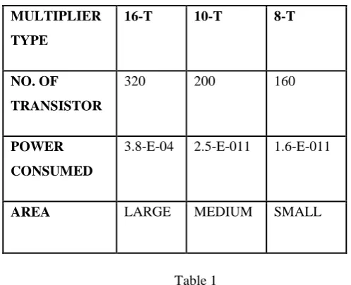
Power and Energy consumptionsare calculated for the conventional array and the proposed multiplier with lownumbers of transistor simulated using T-Spice and the performance of the both multipliers shown in the table.
MULTIPLIER TYPE
16-T 10-T 8-T
NO. OF
TRANSISTOR
320 200 160
POWER CONSUMED
3.8-E-04 2.5-E-011 1.6-E-011
AREA LARGE MEDIUM SMALL
Table 1
6.1 TOTAL POWER
The total power of these two multipliers is calculated using tanner EDTA, T-spice tool. The proposed multiplier
has shown the power improvement than that of conventional multipliers; also the proposed multiplier shows good
performance due to less transistor count to avoid more leakage current.
6.2 TRANSISTOR COUNT
The proposed multiplier has 160 less transistor count than that of the conventional multiplier. These less count
can trade off in area consumption.
147 |
P a g e
Fig.9 Power ComparisonThe total power and numbers of transistor used in circuit is compared and the corresponding wave form is
obtained. Relative graph is shown.
VII. CONCLUSION
In a new design for low power, high performance and low area based array multiplier is proposed with minimal
numbers of transistors. It shows the same functionality than the conventional adder. For higher bit multiplication it
shows better power and area saving. For example, in the proposed 4x4 multiplier it saves 160 MOS transistors. To
study the performance of the multiplier, it is synthesized with different technologies.
REFERENCE
[1] G.Brindha, S.Deepa, “Design of Multiplier using 10t Full Adder,”IJART vol. 2 Issues 2, 2012, 45-48.
[2] Tripti Sharma, K. G. Sharma, Prof.B.P.Singh, “High Performance FullAdder cell: A Comparative Analysis,”
Proceeding of the 2010 IEEEStudents‟ Technology Symposium 3-4 April 2010, IIT Karagphur.
[3] Monhanraj.S, Maheswari.M, “SERF and modified SERF adder for ultra-Low power design techniques,
“International Conference on Communication Technology and System Design 2011.
[4] Raja, B.M.Parabu, K.Thanuskodi, “Design of low power digital Multiplier using dual threshold voltage Adder
module,” International Conference on Communication Technology and System Design 2011.
148 |
P a g e
Shannon-based adder cell,” 2011.[6] Niralakalla Ravi, AnchulaSathish, Dr.TalariJayachandra Prasad and Dr.ThotaSubbaRoa, “A new design for
array multiplier with trade off in Power and area, "May 2011.
[7] C.N.Marimuthu, P.Thangaraj, “Transmission gate based high Performance low power multiplier,” Journal of