Vinay et al. World Journal of Engineering Research and Technology
STUDY AND DESIGN THE PERFORMANCE ANALYSIS OF DIGITAL
MODULATION TECHNIQUES
Vinay R.*1, Yaseen Basha2 and Nagesh K. N.3
P G Student1, Assistant Professor2, HOD and Professor3
Department of ECE, NCET, Bangalore, India.
Article Received on 09/04/2019 Article Revised on 30/04/2019 Article Accepted on 20/05/2019
ABSTRACT
The paper presents study and design the performance of Amplitude
Shift Keying (ASK), Frequency Shift Keying (FSK), Phase Shift
Keying (PSK), Quadrature Phase Shift Keying (QPSK). The design of
these digital modulation techniques is performed by using general
block diagram. The fundamental of the signal is based on quantization, sampling and this
signal is verified in amplitude and time domain. The work is accomplished using Verilog
hardware description language and the performance is done using Xilinx-ISE 14.6 and model
sim 10.4b (Quartus prime 15.1).
KEYWORDS: ASK, FSK, PSK, QPSK, ortho normal.
1. INTRODUCTION
Since last few years ago, there may be some changes which causes the occurrence of large
modification commencing analog modulation along with phase modulation and frequency
modulation accent to the newest techniques in digital modulation. This type of techniques in
digital modulation happen to be the basics and essentials in the communication network such
as mobile network, wireless network, satellite communication network. These modulation
techniques uses digital format in telecommunication system where the modulation of
amplitude, phase, frequency of continuous waveform such as carrier signal uses input signal
which causes the message signal is transmitted known as original signal.[2]
World Journal of Engineering Research and Technology
WJERT
www.wjert.org
SJIF Impact Factor: 5.218*Corresponding Author
Vinay R.
P G Student,Department of
ECE, NCET, Bangalore,
the serial transmission for transferring the message signal.[1]
The main goal is to achieve a simplified and general block diagram of digital modulation
techniques and it is simulated using VERILOG HDL and the output signals are verified and
analyzed using Xilinx-ISE and model simulator (wave).
2. Digital Modulation
There is a lot of development from analog to digital modulation techniques which will
provide the information with more compatible with data assistance with extreme data hostage
in the communications. This will be the main role to use communication in this digital
domain.[1]
It is a process which is similar to the analog modulation of transferring lower frequency
signals such as digital information or bits from computer over a high frequency carrier
signals. These modulations have a baseband signals which will have different levels of
discrete amplitude. The binary signal is represented in terms of logic 0 or 1.[3]
In modulation technique there are 3 major properties which vary the carrier signal.
C(t) = A cos (2π fc t φ)...(1)
Where, A = Amplitude of the signal. fc = Frequency of the signal.
Φ = Phase of the signal.
From the above parameters the variations in the carrier signal existing a larger number of
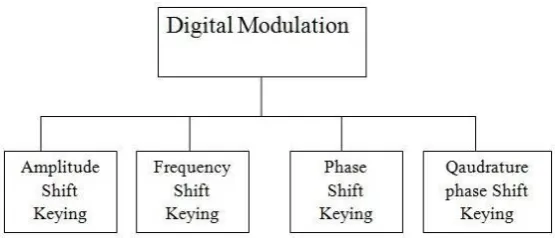
modulation techniques In this modulation they can classified into four types,
I. Amplitude Shift Keying or ASK.
II. Frequency Shift Keying or FSK.
III.Phase Shift Keying or PSK.
Fig 2.1: Types of Digital Modulation Techniques.
2.1Amplitude Shift Keying (ASK)
In Amplitude Shift Keying the amplitude of carrier signal is varied with respect to the
message signal m(t). m(t) is a Modulated carrier and cos wc t is the carrier signal. The
information across the input is a ON/OFF signal and the across output is also ON/OFF
signal.[1]
The ASK signal is given by
s(t) = A m(t) cos (2*Π*fc* t), 0 < t < T...(2)
Where, A = Constant, m(t) = 0 or 1,
fc = carrier frequency, T = bit duration.
2.2Frequency Shift Keying (FSK)
In the digital modulation techniques the Frequency Shift Keying or FSK where the digital
data is transferred by deviating the frequency of carrier signal. In frequency signal the carrier
of phase and amplitude is kept constant while the frequency is varied according to the input
signal which can represent in digital form.[1]
The fsk signal is given by
SFSK = A sin {2 π [fc + m (t) fm] t + Φ0},
0 ≤ t ≤ T...(3)
Where, m(t) = Message signal, T= bit duration, A = Amplitude, fc = Frequency,
Φ0 = Phase of sinusoidal signal.
2.3Phase Shift Keying (PSK)
In phase shift keying modulation technique, during the transmission of data the phase of the
Fig 2.5.1: Block Diagram for Amplitude Shift Keying.[12]
Fig 2.5.3: Block Diagram for Phase Shift Keying.[12]
Fig 3.1: Simulated output for ASK.
The above figure 3.1 shows the simulated output results for amplitude shift keying. The
output will be obtained depending upon the clock frequency selection. For example the given
clock frequency is 142.80 MHz, when the input sequence is high the amplitude gets shifted
similarly, when the input sequence is low there is no change or amplitude is not shifted.
Fig. 3.2: Simulated output for FSK.
The above figure 3.2 shows the simulated output results for frequency shift keying. The
output will be obtained depending upon the clock frequency selection. For example the given
clock frequency is 142.80 MHz, when the input sequence is high the frequency of the signal
is not changed similarly, when the input sequence is low there is change in frequency of the
signal.
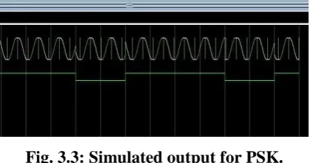
Fig. 3.3: Simulated output for PSK.
The above figure 3.3 shows the simulated output results for phase shift keying. The output
frequency is 142.80 MHz, when the input sequence is high the phase of the signal is shifted
similarly, for low input sequence there is change in the phase of the signal.
Fig. 3.4: Simulated output for QPSK.
The above figure 3.4 shows the simulated output results for quadrature phase shift keying.
The output will be obtained depending upon the clock frequency selection. For example the
given clock frequency is 142.80 MHz, when the input sequence is 00 there is change in phase
of the signal similarly when the input sequence is 01 again phase of the signal is shifted.
3.2 Comparison of different parameters.
Table 1: Existing parameters from reference.[12]
Parameters Values
ASK FSK PSK QPSK
Power 0.039 W 0.040 W 0.04 0W 0.040 W
Number of occupied slices 210 210 72 44
Number of fully used LUT 147 147 56 25
IOB’S 90 90 60 9
Rise time of the clock 9.309ns 10.260ns 9.801ns 9.683ns
Table 2: Proposed Method.
Parameters Values
ASK FSK PSK QPSK
Power 0.014W 0.014W 0.014W 0.014W
Number of occupied slices 119 219 121 117
Number of fully used LUT 124 233 109 111
IOB’S 23 23 23 24
Rise time of the clock 6.73ns 8.31ns 8.29ns 8.29ns
Delay 6.73ns 6.89ns 6.89ns 6.91ns
4 CONCLUSION
The design and performance of digital modulation techniques has been carried out using
model sim and Xilinx ISE simulator. In the proposed method the comparison of various
parameters such as delay, power, rise time, IOB, number of occupied slices, fully used LUT
2. E. A. Lee and D. G. Messerschmitt, “Digital communication”. Springer Science &
Business Media, 2012.
3. S. S. Haykin M. Moher, and T. Song, “An Introduction to Analog and Digital
Communications”. Wiley New York, 1989.
4. B. P. Lathi, “Modern Digital and Analog Communication Systems 3e” Osece. Oxford
university press, 1998.
5. A. B. Carlson and P. B. Crilly, “Communication systems”, Mc Graw Hill International
Edition 5e, 2016.
6. S. M. Alamouti, “A simple transmit diversity technique for wireless communications”
IEEE Journal on selected areas in communications, 1998; 16(8): 1451–1458.
7. Goldsmith, “Wireless communications”. Cambridge university press, 2005.
8. M. Mano, “Digital logic, Computer Design”, Prentice Hall, Inc. New Jersey, 1999;lX(7).
9. F. Quadri and A. D. Tete, “Fpga implementation ofdigital modulation techniques,” in
Communications and Signal Processing (ICCSP), International Conference on. IEEE,
2013; 913–917.
10.Razavi and, “Design of analog CMOS integrated circuits”, 2001.
11.S. Palnitkar, Verilog HDL: “a guide to digital design and synthesis”. Prentice Hall
Professional, 2003; 1.
12.Akshay Sharma and Shubankar Majumdar and Alok naugarhiya” VERILOG BASED
SIMULATION OF ASK, FSK, PSK, QPSK Digital Modulation Techniques”
![Fig 2.5.1: Block Diagram for Amplitude Shift Keying.[12]](https://thumb-us.123doks.com/thumbv2/123dok_us/8362240.1671860/4.595.178.419.490.717/fig-block-diagram-for-amplitude-shift-keying.webp)
![Fig 2.5.3: Block Diagram for Phase Shift Keying.[12]](https://thumb-us.123doks.com/thumbv2/123dok_us/8362240.1671860/5.595.139.461.339.744/fig-block-diagram-phase-shift-keying.webp)