31
Compact Qca Based Serial-Parallel Multiplier For
Signal Processing Applications
Premananda B.S., Bhargav U.K., Kaza Sai Vineeth
Abstract—Quantum-dot Cellular Automata (QCA) is a promising nanoscale technology with great prospect to provide compact circuits with low energy consumption when compared to CMOS technology. The increasing demand for efficient signal processors necessitates the design of adders and multipliers which occupy less area and consume less power. Serial adders are area efficient architectures that can compute n-bit addition with a single adder but takes more time when compared to n-bit parallel adders. Serial-parallel multipliers have simple, regular and scalable structures in contrast to multipliers that implement more complex multiplication algorithms. This paper proposes two novel energy and area efficient 4-bit QCA based serial-parallel multiplier circuits. Initially a QCA based serial adder is designed and then a 2-bit serial-serial-parallel multiplier is realized. This multiplier is scaled up to form a 4-bit serial-parallel multiplier. A Baugh-Wooley (parallel) multiplier is constructed as a case study to illustrate differences between coplanar and multilayer crossovers in QCA. The design and simulation of the QCA circuits are performed using QCADesigner-E. Circuits are evaluated based on cell count, area and energy dissipation. It can be inferred from the simulation results that the proposed 4-bit serial-parallel multipliers have reduced cell count, area and energy dissipation.
Index Terms—QCA, QCADesigner-E, Serial adder, Serial-parallel multiplier, Parallel multiplier.
————————————————————
1.
INTRODUCTION
ADDERS and multipliers are the building blocks of most signal processing blocks such as MAC and FIR filters. The increase in demand for battery powered portable devices leads to the increase in the need for low power and compact circuits. Hence the design of low power and compact adders and multipliers is necessary. A serial-parallel multiplier is a compact multiplier design as it uses serial adders. In a serial-parallel multiplier one input (multiplicand) is given in series and the other input (multiplier) in parallel [1]. Due to the serial input the throughput of the adder is low but as serial-parallel multipliers have regular and scalable structures it makes it ideal for multiplier designs that are area critical but not speed critical. The continuous scaling down of CMOS-based devices in size, over the past few decades, in accordance with Moore's law leads to many different and difficult challenges as recently these devices are becoming more resistant to scaling. One of the biggest challenges faced by transistor-based circuits is power consumption from leakage current due to the increasing threshold voltage and decreasing supply voltage [12]. The search for new technologies led to Quantum-Dot Cellular Automata (QCA) which has appealing features such as lower energy consumption and less cell density [2]. QCA designs offer lower energy and area solutions to the existing CMOS logic. QCA based designs are suitable for fabrication of nano-scale devices. QCA based adders and multipliers are more efficient than CMOS based adders and multipliers as far as area and energy consumption are concerned. The realization of a 2-bit QCA based, multilayer serial-parallel multiplier has been discussed in [2]. This multiplier is directly based of the multiplier schematic designed for conventional transistor-based circuits. As a direct translation from transistor to QCA is not very efficient, the designed multiplier has a very high cell count and area. A three-input coplanar majority gate and inverter structures are discussed in [3]. It is further extended to a single bit coplanar full adder, but no latency or energy dissipation parameters are discussed. This full adder is further improved in [15] by using a multilayer approach. The multilayer approach, though practically less feasible than coplanar wire crossing approach has significant improvement with regards to area and delay. The serial-parallel multiplier in [5] is designed using coplanar wire crossing approach. The multiplier has been designed based on FIR filter equations. The increase in
area and latency with the increase in number of bits of the multiplier is discussed. Due to the co-planar architecture of the multiplier the area consumed were high. A QCA based serial adder (QSA) that used coplanar crossovers has been discussed in [7]. Instead of using conventional 45° and 90° wires for crossovers, QCA property that when two wires that use clocks out of phase by 180° can function as a crossover is used. The coplanar serial-parallel multiplier designed using this technique had a low cell count and area compared to previous coplanar multiplier designs. The failures that occur in QCA design due to electromagnetic noise are discussed in [8]. This failure rate is higher at the cross over points due to sneak noise. A QCA based serial adder was implemented incorporating all the failure parameters. [9] Explores the delay transfers and retiming using QCA characteristics to solve timing issues. The design and analysis of QCA circuits have been studied in recent years. A set of design rules that are necessary for proper timing techniques are discussed in [10]. Clocking techniques for majority gate and QCA wire are discussed. These rules are necessary for getting an output that is non-degraded. Due to high computational and low power requirements in the portable devices, the design of optimized adders and multipliers are necessary in signal processing and communication applications to perform basic operations. QCA based circuit’s offers a novel solution to the low energy and area requirements. The organization of the paper is as follows: Section 2 discusses the basics of QCA technology. In section 3 the design and simulation of QCA based serial adder and serial-parallel multiplier in QCADesigner-E is discussed. In section 4, the results obtained from the simulation of the multipliers are discussed and a comparison has been done with regards to area, cell count and energy dissipation. Section 5 provides conclusions and discusses possible future scope of the work.
2.
QCA BASICS
32 '1' (when one of the electrons is positioned in the top right
site). They have respective polarizations as P = '-1' (logic ‘0’) and P = '+1’ (logic ‘0’) as depicted in the Fig. 1. QCA has two basic gates namely inverter and the majority gate (majority voter) [13]. The inverter is the result of placing the cells such that their vertices are touching as shown in Fig. 2. The cells positioned in such a way that their vertices are in contact tend to have opposite polarizations due to the electrostatic repulsion between the electrons of the other cell [10]. A majority voter consists of five cells: one device cell (center cell), three inputs and an output cell as shown in Fig. 3. Majority voter is driven by three inputs drivers A, B and C. A two input AND operation can be performed by the majority voter when the one of the inputs is fixed to logic '0' and when the one of the inputs is fixed to logic '1' the majority voter performs a two input OR operation. A QCA wire is shown in Fig. 4. The data provided at the input stage propagates through the wire through electrostatic repulsions to the output. As QCA uses electrostatic repulsions to propagate the logic states, there is no guarantee that the data will flow in that direction. To ensure that proper data flow takes place QCA circuit clocking is introduced. QCA based circuits have a four-phased clocking namely switch, hold, release and relax as illustrated in Fig. 5. These four phases are generated by traveling electric field wave perpendicular to the QCA plane. The various clock zones are represented by four different colors. Clock 0 is represented by green, clock 1 by pink, clock 2 by blue and clock 3 by white. Each clocking zone has a phase shift of 900 with respect to the adjacent ones. Each cell in a clocking zone behaves as latch. The assignment of clocks needs to be appropriate for efficient QCA design. The proper assignment of the clocking zones must follow the design rules discussed in [8]. Crossover types provide an advantage in circuit design in QCA as it offers a certain amount of design flexibility. QCA technology has two types of crossover. One, multilayer crossover and the other is coplanar crossover as depicted in Fig. 6(a) and Fig. 6(b) respectively. Clock 0 is represented by green, clock 1 by pink, clock 2 by blue and clock 3 by white. Each clocking zone has a phase shift of 900 with respect to the adjacent ones. Each cell in a clocking zone behaves as latch. The assignment of clocks needs to be appropriate for efficient QCA design. The proper assignment of the clocking zones must follow the design rules discussed in [8].
Fig. 1. QCA cell.
Fig. 2. QCA Inverter [8]
Fig. 3. Majority Voter [11]
Fig. 4. QCA Wire
Fig. 5. QCA Clocking scheme [10]
33 constructed in the bottom layer. The crossover wires are
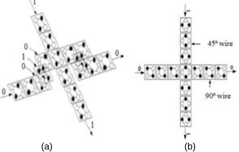
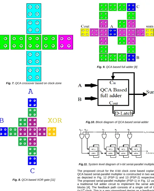
placed on the top layer and the mid-layers are used as a connection between the layers. The middle layers act as active components of the circuit. This type of crossover consumes less area compared to coplanar circuits. The disadvantage of coplanar crossing can be overcome by using wire crossings of wire that are 180° out of phase as shown in Fig. 7. Since the four clocks are out of phase by 90°, clock-0 and clock-2 can be used for crossover or clock-1 and clock-3 may be used. The serial-parallel multiplier proposed uses this type of clocking scheme to achieve optimal results.
(a) (b)
Fig. 6(a) Multilayer crossing (b) Coplanar crossing
3.
DESIGN AND SIMULATION OF QCA BASED
MULTIPLIER
The QCA basic gates, the majority voter and inverter have been discussed in the previous section. Using these QCA basic gates, AND gate and OR gate is implemented and are used for the realization of the QCA based full adder. A single bit multiplier is a logical AND. A 2-bit serial-parallel multiplier consists of two AND gates and a serial adder. A 4-bit serial-parallel multiplier is a scaled-up version of the designed 2-bit multiplier and consists of four AND gates and three serial adders. The partial products are computed and added to the sum. There are two types of simulation integrated in QCADesigner, coherence vector simulation and bistable approximation simulation. Coherence vector though computationally intensive is preferred over bistable approximation because of the higher accuracy results obtained. The QCADesigner-E offers Coherence vector simulation engine with energy dissipation which gives energy dissipation values of the QCA circuit.
3.1 The Layout for QCA based Full Adder
A QCA based full adder is constructed using the XOR gate shown in Fig. 8. This design uses only 14 cells to construct the XOR gate. The proposed full adder follows the logical expressions (1) and (2).
Sum = A ⊕ B ⊕ C (1) Cout = Majority (A; B; C) = AB + BC + CA (2)
The full adder constructed using XOR gate (Fig. 8) is shown in Fig. 9. This QCA based full adder has three inputs: ‘A’, ‘B’ and ‘C’. The inputs are fed to an XOR gate and a majority voter that are aligned back to back for maximum area efficiency. The drawback of this construction is that an input is present in the
center of the adder. This input node is not very accessible when this full adder is scaled up. This limitation can be overcome by using a few extra cells to make sure that the input node is available easily. A serial adder is illustrated in Fig. 10. The output carry of the full adder is feedback to its carry input using a D-latch. In QCA a D-latch is a simple QCA wire. The serial adder is efficient adder architecture when high speed is not a constraint. It uses one adder to compute n-bit addition in n clock cycles.
3.2 The Layout for Parallel Multiplier
In a parallel multiplier both the multiplicand and the multiplier bits are fed in parallel [14]. Two 4 × 4 Baugh-Wooley (parallel) multipliers having the same architecture with different crossover is discussed in [11]. One of these multipliers is constructed using multilayer crossing and the other using coplanar crossing. In a parallel multiplier as both inputs are fed in parallel there is minimal delay when compared to serial-parallel multiplier where the serial input causes additional delay. This makes parallel multiplier ideal for speed critical circuits that are ready to make a trade-off in terms of area.
3.3 QCA based Serial-Parallel Multiplier
34
Fig. 7. QCA crossover based on clock-zone
Fig. 8. QCA based XOR gate [11]
Fig. 9. QCA based full adder [8]
Fig.10. Block diagram of QCA based serial-adder
Fig.11. System level diagram of n-bit serial-parallel multiplier
35
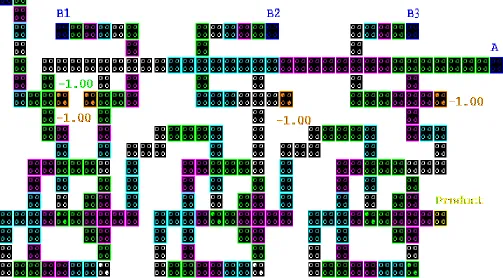
Fig. 12. Layout of the first proposed QCA circuit for 4-bit Serial-parallel multiplier (PSP-1).
36
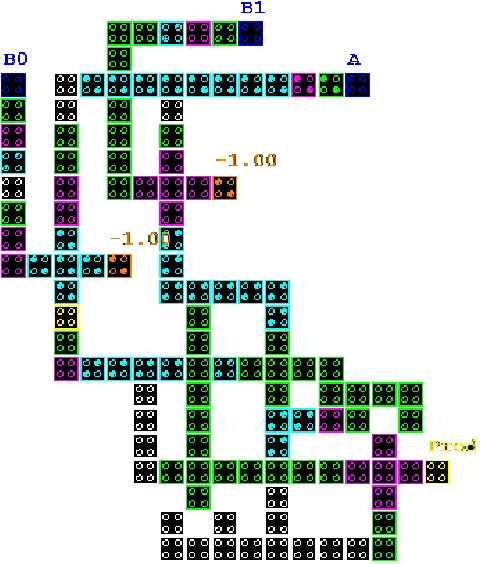
Fig.14. 2-bit QCA based serial-parallel multiplier
4.
RESULTS AND DISCUSSION
Results of the simulation of the serial adders, parallel multipliers and proposed serial-parallel multipliers are presented in this section obtained using the CAD tool QCA Designer. Serial adders are the fundamental building blocks of serial parallel multipliers. Reduction in the adder size will result in a subsequent reduction of the scaled-up circuits. Comparisons of various serial adder architectures based on cell count and area that have been discussed in the literature are listed in Table I. It can be inferred from Table I that circuits with conventional coplanar wire crossings have the highest area when compared to multilayer wire crossing circuits. Clock zone based coplanar wire crossings lead to circuits having the least cell count and area.
Table I. Serial adder comparison
Serial adder Cell count Area
(µm2) Layer Type
[7] 222 0.38 Conventional Coplanar
[2] 155 0.19 Conventional Coplanar
[8] 79 0.089 Multilayer
[6] 73 0.06 Clock zone based
Coplanar Proposed
Serial adder 38 0.03
Clock zone based Coplanar
From Table I, it can be analyzed that due to a compact XOR gate and the use of clock zone based coplanar wire crossing, the proposed serial adder has reduction of 82.88 % in cell count and 92.1 % in area compared to conventional coplanar crossover based serial adder in [7]. Also, proposed serial
adder has 51.89 % improvement in terms of cell count and 66.29 % improvement in terms of area when compared to the multilayer serial adder in [8]. In serial adders, by modifying the XOR gate there is a significant decrease in the size of the adder. Subsequently using modified serial adder to construct the proposed multiplier circuit results in a decrease in the area and cell count of the multiplier. Simulation results obtained from QCADesigner of the proposed-1 circuit is shown in Fig. 15. Coherence vector simulation engine with 50000 samples and all other parameters set at default values are used. An n× n multiplier receives a serial input of one bit and a parallel input of n-bits in one clock cycle and generates a 2n-bit serial output. The designed multiplier is analyzed for various inputs. The simulated outputs are illustrated for inputs ‘A’ = (1111)2 and ‘B’ = (1111)2. Here input B is fed in parallel while input A is given in serial. The multiplier output is (11100001)2. The output of proposed-2 serial-parallel multiplier for the same inputs is identical. Hence, the simulation output of the proposed-2 multiplier is not included in the paper. A comparison of coplanar and multilayer parallel multiplier is depicted in Table II. It can be inferred from Table II, that by converting multilayer architecture to coplanar clock zone based crossover architecture and without modifying the adders; 14.41 % improvement in cell count and 14.49 % reduction in energy dissipation can be achieved. The changing of the crossover does not change the structure of the multiplier. Hence, there is only a slight change in the area but, since the cell count decreases there is a reduction in the energy dissipation of the multiplier. The representation of energy and area of parallel multiplier is shown in Fig. 16.
Table II. Comparison of multilayer and coplanar layer type parallel multipliers
Parallel Multiplier
Cell count
Area
(µm2) Energy (nW) Layer Type
[11] 1956 1.87 5.59e-01 Multilayer
Proposed
multiplier 1674 1.8
4.78e-01 Clock zone based Coplanar
37
Fig. 16. Multilayer and coplanar Baugh-Wooley parallel multiplier
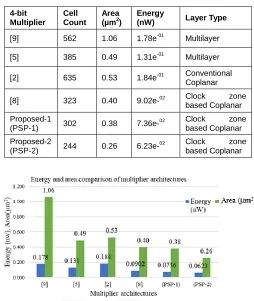
Table III shows the comparison of various serial-parallel multipliers that have been discussed in literature over the years along with the parallel multiplier [11]. It can be inferred from Table III that a parallel multiplier occupies more area and consumes more energy when compared to a serial-parallel multiplier. Parallel multiplier has less latency when compared to serial-parallel multipliers that make it desirable for speed critical circuits. Serial-parallel multiplier architectures in [2] and [8] are coplanar multipliers while multiplier architectures in [5] and [9] are multilayer multipliers. Generally coplanar circuits have more cell count but the use of modified XOR gate in the proposed architecture reduces the cell count and the area. The proposed-1 serial-parallel architecture has an 84.56 % improvement in terms of cell count and 86.83 % improvement in energy dissipation in comparison with the parallel multiplier [11]. The proposed (PSP)-1 multiplier architecture an incremental improvement over the multiplier proposed in [8]. The multiplier also helps in the effective retiming of the cells as the common fixed polarities arrive at both majority gates at the same time. The effective use of retiming techniques reduces the energy consumed. The PSP-2 multiplier architecture uses a different XOR gate for the serial adder than the one in proposed-1 architecture. Due to the use of the modified XOR gate and clock zone based coplanar crossing, there is a 92.1 % decrease in area of the serial adder over a conventional adder. This results in an overall decrease in the area and cell count of the serial-parallel multiplier. The PSP-1 multiplier shows a 52.44 % improvement in cell count when compared to [2] and both multipliers use coplanar crossing and 46.26 % improvement in comparison with the multilayer architecture in [9]. An 18 % improvement in energy dissipation with respect to [8] is observed and 43.81 % improvement in energy dissipation with respect to [5]. From Table III, it can be inferred that using the modified XOR gate in the serial-parallel multiplier leads to 56.58 % reduction in cell count when compared to the multilayer serial parallel multiplier in [9] and 19.20 % reduction in cell count with respect to the coplanar serial-parallel multiplier. Hence the proposed serial parallel multipliers are better than the existing multipliers in literature. The energy dissipations of the simulated multipliers are depicted in Fig. 17. Minimizing the number of cells with fixed polarities by providing a common fixed cell wherever required reduces the cell count and energy considerably in the proposed-1 multiplier. The use of the much smaller adder in proposed-2 multiplier results in a 19.2 % decrease in the cell count and a 15.35 % decrease in area in comparison with
proposed-1. Energy dissipated can also be related to power dissipation of the circuits.
Table III. Comparison of various Serial-parallel Multipliers 4-bit Multiplier Cell Count Area (µm2)
Energy
(nW) Layer Type
[9] 562 1.06 1.78e-01 Multilayer
[5] 385 0.49 1.31e-01 Multilayer
[2] 635 0.53 1.84e-01 Conventional Coplanar
[8] 323 0.40 9.02e-02 Clock zone based Coplanar
Proposed-1
(PSP-1) 302 0.38
7.36e-02 Clock zone based Coplanar
Proposed-2
(PSP-2) 244 0.26
6.23e-02 Clock zone based Coplanar
Fig. 17. Comparison of various multiplier architectures.
5.
CONCLUSIONS AND FUTURE SCOPE
38
ACKNOWLEDGEMENTS
All acknowledgments (if any) should be included at the very end of the paper before the references and may include supporting grants, presentations, and so forth.
Conflict of Interest: None
REFERENCES
[1] F.S. Torres, R. Wille, P. Niemann, and R. Drechsler (2018). An Energy-Aware Model for the Logic Synthesis of Quantum-Dot Cellular Automata. IEEE Transactions on CAD of Integrated Circuits and Systems, 1-11.
[2] K. Walus, T.J. Dysart, G. A. Jullien, and R. A. Budiman (2004). QCA Designer: A Rapid Design and Simulation Tool for Quantum-Dot Cellular Automata IEEE Transactions on Nanotechnology, 3: 26-31.
[3] C. S. Lent, P. D. Tougaw, W. Porod, and G. H. Bernstein (1993). Quantum Cellular Automata. Nanotechnology, 4(1): 49-58. [4] Premananda B. S., Bhargav U. K., and Kaza Sai Vineeth
(2018). Design and Analysis of Compact QCA Based 4-Bit Serial-Parallel Multiplier. Proceedings of the 2nd IEEE International Conference on Electrical, Electronics, Communication, Computer Technologies and Optimization Techniques, 1014 to 1018. (in press).
[5] K. Kim, K. Wu, and R. Karri (2007) The Robust WCA Adder Designs using Composable QCA Building Blocks. IEEE Transactions on CAD of Integrated Circuits and Systems. 26 (1), 176-183.
[6] Namita and T. N. Sasamal (2017) Design of 4-Bit Serial-Parallel Multiplier in Quantum-Dot Cellular Automata. Proceedings of the IEEE International Conference on Signal Processing, Computing and Control. 1-4.
[7] W. Liu, L. Lu, M. O'Neill, and E. E. Swartzlander, (2011). Design Rules for Quantum-Dot Cellular Automata. IEEE International Symposium on Circuits and Systems. 2361-2364.
[8] D. Abedi, and G. Jaberipur, (2015). Coplanar QCA Serial Adder and Multiplier via Clock-Zone based Crossover. Proceedings of the IEEE CSI International Symposium on Computer Architecture and Digital Systems. 1-4.
[9] I. Hänninen and J. Takala. (2010). Binary Adders on Quantum-Dot Cellular Automata. Journal of Signal Processing Systems. 58(1): 87-103.
[10]I.E. Arani and A. Rezai, (2018). Novel Circuit Design of Serial-parallel Multiplier in Quantum-Dot Cellular Automata Technology. Journal of Computational Electronics. 1-9.
[11]Kalogeiton et al., (2017). Programmable Crossbar Quantum-Dot Cellular Automata Circuits. IEEE Transactions on Computer-Aided Design of Integrated Circuits and Systems. 36(8): 1367-1380.
[12]Premananda B. S., and Ganavi M. G. (2019). Performance Analysis of Low Power 8-Tap FIR Filter using PFAL. International Journal of Innovative Technology and Exploring Engineering. 8(8): 365-374.
[13]K. Navi, R. Farazkish, S. Sayedsalehi, and M. R. Azghadi (2010). A New Quantum-Dot Cellular Automata Full-Adder. Journal of Microelectronics. 41(12): 820-826.
[14]Vinay B. Biradar, Vishwas P.G., Chetan C.S., and Premananda B. S., (2017). Design and Performance Analysis of Modified Unsigned Braun and Signed Baugh Wooley Multiplier. Proceedings of the 2nd IEEE International Conference on Electrical, Electronics, Communication, Computer Technologies and Optimization Techniques., pp. 1-5.
[15]H. Cho, and E.E. Swartzlander (2009). Adder and Multiplier Design in Quantum-Dot Cellular Automata. IEEE Transactions
![Fig. 2. QCA Inverter [8]](https://thumb-us.123doks.com/thumbv2/123dok_us/8635975.1425683/2.612.316.566.53.634/fig-qca-inverter.webp)