10
An Efficient Implementation of Advanced Encryption
Standard on the Coarse-grained Reconfigurable Architecture
Hung K. Nguyen
*,
Xuan-Tu Tran
SIS Laboratory, VNU University of Engineering and Technology, 144 Xuan Thuy road, Cau Giay district, Hanoi, Vietnam
Abstract
The Advanced Encryption Standard (AES) is currently considered as one of the best symmetric-key block ciphers. The hardware implementation of the AES for hand-held mobile devices or wireless sensor network nodes is always required to meet the strict constraints in terms of performance, power and cost. Coarse-grained reconfigurable architectures are recently proposed as the solution that provides high flexibility, high performance and low power consumption for the next-generation embedded systems. This paper presents a flexible, high-performance implementation of the AES algorithm on a coarse-grained reconfigurable architecture, called MUSRA (Multimedia Specific Reconfigurable Architecture). First, we propose a hardware-software partitioning method for mapping the AES algorithm onto the MUSRA. Second, the parallel and pipelining techniques are considered thoughtfully to increase total computing throughput by efficiently utilizing the computing resources of the MUSRA. Some optimizations at both loop transformation level and scheduling level are performed in order to make better use of instruction-, loop- and task- level parallelism. The proposed implementation has been evaluated by the cycle-accurate simulator of the MUSRA. Experimental results show that the MUSRA can be reconfigured to support both encryption and decryption with all key lengths specified in the AES standard. The performance of the AES algorithm on the MUSRA is better than that of the ADRES reconfigurable processor, Xilinx Virtex-II, and the TI C64+ DSP.
Received 24 November 2015, revised 06 January 2015, accepted 13 January 2016
Keywords: Coarse-grained Reconfigurable Architecture (CGRA), Advanced Encryption Standard (AES), Reconfigurable Computing, Parallel Processing.
1. Introduction*
The fast development of the communication technology enables the information to be easily shared globally via the internet, especially with the Internet of Things (IoT). However, it also raises the requirement about the secure of the information, especially the sensitive data such
as password, bank account, personal
information, etc. One method to protect the sensitive data is using symmetric-key block cipher before and after sending it over the
________
*Corresponding author. E-mail.: [email protected]
network. The Advanced Encryption Standard (AES), which has been standardized by the National Institute of Standard and Technology (NIST) [1], is currently considered as one of the best symmetric-key block ciphers. With the block size of 128 bits and the variable key length of 128 bits, 192 bits or 256 bits, the AES has been proved to be a robust cryptographic algorithm against illegal access.
power consumption, increasing application performance, shortening time-to-market, and simplifying the updating process. Besides, these systems are often designed not only for a specific application but also for multiple applications. Such sharing of resources by several applications makes the system cheaper and more versatile. Application Specific Integrated Circuits (ASICs), Digital Signal Processors (DSPs), and Application-Specific Instruction Set Processors (ASIPs), have been used for implementing the mobile multimedia systems. However, none of them meets all of the above challenges [2]. The software implementation of the AES algorithm by using processors (e.g. [3]) are usually very flexible and usually targets at the applications at where flexibility has a higher priority than the implementation efficiency in terms of power consumption, area, and performance. In contrast, the ASIC implementation of the AES algorithm (e.g. [4]) usually offers the optimized performance and power consumption. However, the drawback of ASIC is lower flexibility. Moreover, the high price for designing and manufacturing the chip masks is becoming increasingly an important factor that limits the
application scope of ASIC. Recently, a very
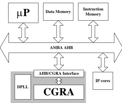
promising solution is the reconfigurable computing systems (e.g. Zynq-7000 [5], ADRES [6], etc.) that are integrated many heterogeneous processing resources such as
software programmable microprocessors (P),
hardwired IP (Intellectual Property) cores, reconfigurable hardware architectures, etc. as shown in Figure 1. To program such a system, a
target application is first represented
intermediately as a series of tasks that depends on each other by a Control and Data Flow Graph (CDFG) [7], and then partitioned and mapped onto the heterogeneous computational and routing resources of the system. Especially, computation-intensive kernel functions of the application are mapped onto the reconfigurable hardware so that they can achieve high performance approximately equivalent to that of ASIC while maintaining a degree of flexibility close to that of DSP processors. By
dynamically reconfiguring hardware,
reconfigurable computing systems allow many
hardware tasks to be mapped onto the same hardware platform, thus reducing the area and power consumption of the design [8].
CGRA
AHB/CGRA Interface
DPLL
AMBA AHB
P
Data Memory Instruction MemoryIP cores
Figure 1.System-level application model of CGRA.
reconfiguration by enabling the hardware fabrics to be reconfigured into different functions even if the system is working.
In this paper, we proposed a solution for implementing the AES algorithm on the platform of the MUSRA-based system. The AES algorithm is firstly analyzed and optimized,
and then HW/SW (Hardware/Software)
partitioned and scheduled to be executed on the MUSRA-based system. The experimental results show that our proposal achieves the throughput of 29.71 instructions per cycle in
average. Our implementation has been
compared to the similar works on ADRES reconfigurable processor [6], Xilinx Virtex-II
[11], and TI C64+ DSP [3]. Our
implementation is about 6.9 times, 2.2 times, and 1.6 times better than that of TI C64+ DSP, Xilinx Virtex-II, and ADRES, respectively.
The rest of the paper is organized as follows. The MUSRA architecture and the AES algorithm are presented in Section 2 and Section 3, respectively. Section 4 presents the mapping the AES algorithm onto the MUSRA-based system. In Section 5, simulation results and the evaluation of the AES algorithm on the MUSRA-based system in terms of flexibility and performance are reported and discussed. Finally, conclusions are given in Section 6.
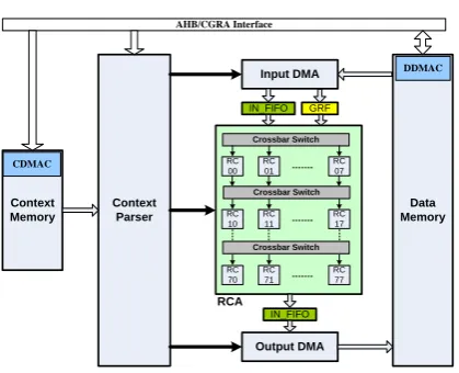
2. MUSRA Architecture
2.1.Architecture Overview
Context Parser Context
Memory
Input DMA
Output DMA
Data Memory
RCA
Crossbar Switch
RC 00
RC 01
RC 07
RC 10
RC 11
RC 17
RC 70
RC 71
RC 77 Crossbar Switch
Crossbar Switch
IN_FIFO
IN_FIFO GRF
AHB/CGRA Interface
CDMAC
DDMAC
Figure 2. MUSRA architecture.
The MUSRA is composed of a
Reconfigurable Computing Array (RCAs), Input/Output FIFOs, Global Register File (GRF), Data/Context memory subsystems, and DMA (Direct Memory Access) controllers, etc. (Figure 2). Data/Context memory subsystems consist of storage blocks and DMA controllers (i.e. CDMAC and DDMAC). The RCA is an
array of 88 RCs (Reconfigurable Cells) that
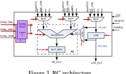
can be configured partially to implement computation-intensive tasks. The input and output FIFOs are the I/O buffers between the data memory and the RCA. Each RC can get the input data from the input FIFO or/and GRF, and store the results back to the output FIFO. These FIFOs are all 512-bit in width and 8-row in depth, and can load/store sixty-four bytes or thirty-two 16-bit words per cycle. Especially, the input FIFO can broadcast data to every RC that has been configured to receive the data from the input FIFO. This mechanism aims at exploiting the reusable data between several iterations. The interconnection between two neighboring rows of RCs is implemented by a crossbar switch. Through the crossbar switch, an RC can get results that come from an arbitrary RC in the above row of it. The Parser decodes the configuration information that has been read from the Context Memory, and then generates the control signals that ensure the execution of RCA accurately and automatically.
DATAPATH
MUX MUX
LOR MUX
A B
C MU
X
In
p
u
tF
IF
O
P
R
E
_
L
IN
E
In
p
u
tF
IF
O
P
R
E
_
L
IN
E
In
p
u
tF
IF
O
OUT_REG
LOR_input
LOR_output
PE_OUT
P
R
E
_
L
IN
E
LOR_OUT PE
CLK RESETN
A_IN B_IN
C
_
IN
Config._Addr Config. Data
ENABLE
G
R
F
s
Cnfig. REGs
Layer 1 Config. REGs Layer 0 Config._ENB
Figure 3. RC architecture.
The data processed by RCA are classified into two types: variables are streamed into the RCA through the input FIFO meanwhile constants are fed into the RCA via either GRF for scalar constants or LOR array for array constants. The constant type is again classified into global constants and local constants. Global constants are determined at compile-time therefore they are initialized in context memory of the MUSRA at compile-time and loaded into GRF/LORs while configuring the RCA. Local constants (or immediate values) are not determined at compile-time, but are the results generated by other tasks at run-time, therefore, they need to be loaded dynamically into GRF/LCRs by configuration words.
2.2.Configuration Model
The configuration information for the MUSRA is organized into the packets called context. The context specifies a particular operation of the RCA core (i.e. the operation of each RC, the interconnection between RCs, the input source, output location, etc.) as well as the control parameters that control the operation of the RCA core. The total length of a context is 128 32-bit words. An application is composed of one or more contexts that are stored into the context memory of the MUSRA.
The function of the MUSRA is
reconfigured dynamically in run-time according to the required hardware tasks. To deal with the
huge configuration overhead in the
reconfigurable hardware, the proposed design of the MUSRA supports a mechanism to pre-load and pre-decode the configuration context from the context memory to the configuration layers in the RCA. By this method, the
configuration of the MUSRA can take place behind the execution of the RCA. As a result, once the RCA finishes calculating with the current context, it can be immediately changed into the next context.
2.3.Execution Model
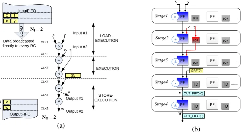
It is a well-known rule of thumb that 90% of the execution time of a program is spent by 10% of the code of LOOP constructs [9]. These LOOP constructs are generally identified as kernel loops. Most of them have computation-intensive and data-parallel characteristics with high regularity, so they can be accelerated by hardware circuits. The MUSRA architecture is basically the such-loop-oriented one. By mapping the body of the kernel loop onto the RCA, the RCA just needs configuring one time for executing multiple times, therefore it can improve the efficiency of the application execution. Executing model of the RCA is the pipelined multi-instruction-multi-data (MIMD) model. In this model, each RC can be configured separately to a certain operation, and each row of RCs corresponds to a stage of a pipeline. Multiple iterations of a loop are possible to execute simultaneously in the pipeline.
For purpose of mapping, a kernel loop is first analyzed and loop transformed (e.g. loop unrolling, loop pipelining, loop blocking, etc.) in order to expose inherent parallelism and data locality that are then exploited to maximize the
computation performance on the target
+
&
-x y
× CLK1
CLK2
CLK3
CLK4
CLK5
LOAD - EXECUTION
STORE-EXECUTION z
v InputFIFO
x y z
L
O
A
D N
I = 2
A
CLK6 w
OutputFIFO v
w 0 1
Output #1
Output #2 NO = 2
Data broadcasted directly to every RC
Input #1
Input #2
35 t
t
EXECUTION
(a)
PE
LOR
PE
PE
PE TD
PE
PE
PE LOR
PE TD
x y
×
-+
&
Stage1
Stage2
Stage3
Stage4
z LOR
LOR LOR
LOR
PE TD PE TD
A
Stage4
w
t
GRF(0)
OUT_FIFO(0)
OUT_FIFO(0)
v
(b)
Figure 4. (a) DFG representation of a simple loop body, and (b) its map onto RCA.
The execution of a loop is scheduled so that the different phases of successive iterations are overlapped each other as much as possible. Scheduling also needs to ensure that there are not any conflicts between resources as multiple phases take place simultaneously.
Parallel processing increases not only the computation performance but also the pressure on the data bandwidth. The system’s bandwidth is necessary to ensure that data is always available for all resources running concurrently without the IDLE state. One way to increase data availability is to exploit the data locality that refers to capability of data reuse within a short period of time [12]. Exploiting the data locality has the potential to increase the processing efficiency of the system because the data can be cached in the internal memory for reuse later, thus reducing stalled times due to
waiting for external memory accesses.
Moreover, the data reuse also has the potential to minimize the number of access to external memory, thus achieves a significant reduction in the power consumption [13]. Compared with the execution model in [14], the MUSRA’s execution model exploits the overlapping data between two successive iterations, so it can enhance the performance and reduce the input data bandwidth [10]. In this model, RCA core
can start computing as soon as the data of the first input appears on the input of the RCA, so LOAD phase and EXECUTION phase of the same iteration can happen simultaneously. In other words, our execution model allows overlapping three phases LOAD, EXECUTION, STORE of the same iteration as much as possible. As shown in Figure 4, an iteration of RCA core in the MUSRA’s model is started by LOAD-EXECUTION phase, and then is EXECUTION phase, finally finished by STORE-EXECUTION phase. On the other hand, this model also allows the data of the next iteration be LOADed simultaneously with the data of the current iteration, so it maximizes not only the level of overlapping between the consecutive iterations but also the data reuse [10].
3. Advanced Encryption Standard
During the cipher process, the 128-bit input block is arranged into a 4×4 matrix of bytes so that the first four bytes of a 128-bit input block are located at the first column in the 4×4 matrix; the next four bytes are located at the second column, and so on. At the output of the last round, the 4×4 matrix of bytes is rearranged into a 128-bit output block. This 4×4 matrix is referred to as the state array in the context of the AES algorithm. The AES standard supports three types of key length, including 128, 196 or 256 bits. The number of rounds to be executed in an AES encryption or decryption process is dependent on the used key length as shown in Eq.(1). The round keys are derived from the
original key thank to the key expansion unit.
6 32
_
+
Key Length
n (1)
Add Round Key
Round 1
Round 2
Round n
K
ey
E
x
p
a
n
si
o
n
w0 – w3
w4 – w7
w8 – w11
w4n – w4n+3
w0 – w3
w4 – w7
w8 – w11
w4n – w4n+3
Round n
Round (n – 1)
Round (n – 2)
Add Round Key 128-bit Plaintext
block
128-bit Ciphertext block
128-bit Plaintext block
128-bit Ciphertext block 128/192/256-bit
Key
Encryption Decryption
Figure 5. The overall structure of AES algorithm [1].
Substitute Bytes
Shift Rows
Mix Columns
Add Round Key Round Key
Inverse Mix Columns
Add Round Key
Inverse Substitute Bytes
Inverse Shift Rows
Round Key
(a) Encryption Round (b) Decryption Round
Figure 6. The overall structure of a round.
Except for the last round, all rounds are identical and including four steps as shown in Figure 6. Notice that the last round (Round n) does not have “Mix Columns” and “Inverse Mix Columns” for the encryption and the decryption, respectively. Also notice that the sequence at where the steps are performed is different for the encryption and the decryption.
4. Implementation
Motivated by the demand of higher throughput and flexibility, as well as low power consumption for the applications of video conference, security IP camera, etc. in this section we are going to describe our
optimization method for improving the
performance of the AES algorithm on the architecture of the MUSRA-based system. In the work, we have mapped both the AES encryption and AES decryption with all options of key length onto the MUSRA-based system. However, for simplifying the presentation in this section, we will focus on the AES encryption and assume that the key length is 128 bits. We have started with the C-software implementation of the AES algorithm and then pay attention on analyzing the source code to indentify computation-intensive loops of the C-software. Besides, since no more parallel is available in the application when processing a single block, the loop transformation and source-level transformation are applied to kernel loops to improve parallelism. Next, the kernel loops are represented intermediately by DFGs and mapped onto RCA to increase the total computing throughput. Finally, we propose a scheduling scheme to manage the dynamically reconfigurable operation of the system. The scheduling scheme also takes
charge of synchronizing the data
communication between tasks, and managing the conflict between hardware resources.
4.1.Hardware/Software Partition
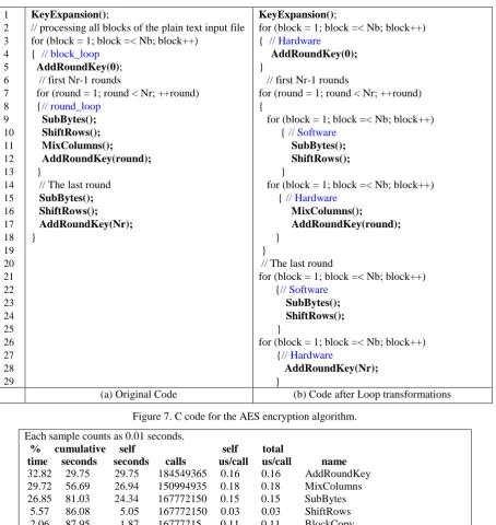
The structure of the AES encryption algorithm in Figure 5 can be modeled by the C source code as shown in Figure 7(a). The AES encryption program is represented by two FOR
1 2 3 4 5 6 7 8 9 10 11 12 13 14 15 16 17 18 19 20 21 22 23 24 25 26 27 28 29
KeyExpansion();
// processing all blocks of the plain text input file for (block = 1; block =< Nb; block++)
{ // block_loop
AddRoundKey(0); // first Nr-1 rounds
for (round = 1; round < Nr; ++round) {// round_loop
SubBytes(); ShiftRows(); MixColumns();
AddRoundKey(round);
}
// The last round SubBytes(); ShiftRows(); AddRoundKey(Nr);
}
KeyExpansion();
for (block = 1; block =< Nb; block++) { // Hardware
AddRoundKey(0);
}
// first Nr-1 rounds
for (round = 1; round < Nr; ++round) {
for (block = 1; block =< Nb; block++) { // Software
SubBytes(); ShiftRows();
}
for (block = 1; block =< Nb; block++) {// Hardware
MixColumns();
AddRoundKey(round);
} }
// The last round
for (block = 1; block =< Nb; block++) {// Software
SubBytes(); ShiftRows();
}
for (block = 1; block =< Nb; block++) {// Hardware
AddRoundKey(Nr);
}
(a) Original Code (b) Code after Loop transformations
Figure 7. C code for the AES encryption algorithm.
Each sample counts as 0.01 seconds.
% cumulative self self total
time seconds seconds calls us/call us/call name 32.82 29.75 29.75 184549365 0.16 0.16 AddRoundKey 29.72 56.69 26.94 150994935 0.18 0.18 MixColumns 26.85 81.03 24.34 167772150 0.15 0.15 SubBytes 5.57 86.08 5.05 167772150 0.03 0.03 ShiftRows 2.06 87.95 1.87 16777215 0.11 0.11 BlockCopy 1.86 89.64 1.69 16777215 0.10 5.23 Cipher 0.82 90.38 0.74 main
0.00 90.38 0.00 40 0.00 0.00 getSBoxValue 0.00 90.38 0.00 1 0.00 0.00 KeyExpansion
Figure 8. Profiling result by using GNU profiler.
round_loop as shown in Figure 7(a). There are five functions in this program. Where,
KeyExpansion() implements the function of
Key Expansion unit; SubBytes(), ShiftRows(),
MixColumns(), and AddRoundKey() implement steps of an encryption round. In order to
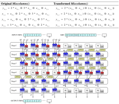
Table 1. Optimizing MixColumns() function
Original Mixcolumns() Transformed Mixcolumns()
c c c c
c x x x x
y0, 2* 0, 3* 1, 2, 3, y0,c 2*(x0,c x1,c) (x1,c (x2,c x3,c))
c c c
c
c x x x x
y1, 0, 2* 1, 3* 2, 3, y1,c 2*(x1,c x2,c) (x2,c (x0,c x3,c))
c c
c c
c x x x x
y2, 0, 1, 2* 2, 3* 3, y2,c 2*(x2,c x3,c) (x3,c (x0,c x1,c))
c c
c c
c x x x x
y3, 3* 0, 1, 2, 2* 3, y3,c 2*(x3,c x0,c) (x0,c (x1,c x2,c))
XOR LOR XOR PE x0 x1 Stage1 Stage2 Stage3 Stage4 XOR LOR Stage5 t0 y0 SLL XOR LOR Stage6 XOR LOR XOR PE x1 x2 XOR LOR t1 SLL XOR LOR XOR LOR XOR PE x2 x3 XOR LOR t2 SLL XOR LOR XOR LOR XOR PE x3 x0 XOR LOR t3 SLL XOR LOR PE LOR SRL MUL LOR LOR LOR XOR LOR AND PE LOR PE LOR SRL MUL LOR LOR LOR XOR LOR AND PE LOR PE LOR SRL MUL LOR LOR LOR XOR LOR AND PE LOR PE LOR SRL MUL LOR LOR LOR XOR LOR AND PE LOR
x3 x0 x1 x2
LOR LOR LOR LOR
t0 GRF(0) t1 GRF(0) t2 GRF(0) t3 GRF(0)
GRF(1) GRF(1)
GRF(1) GRF(1)
LOR LOR LOR LOR
LOR LOR LOR LOR
GRF(1) GRF(1) GRF(1) GRF(1)
GRF(2) GRF(2) GRF(2) GRF(2)
v0 v1 v2 v3
v0 v1 v2 v3
GRF(6) GRF(5)
GRF(4) GRF(3)
w0 w1 w2 w3
w0 w1 w2 w3
y0 y1 y2 y3
y1 y2 y3
OUTPUT FIFO
0 31
x0 x1 x2 x3
INPUT FIFO
0 31
0x07 0x01 0x1B K0
GRF
0 31
K1 K2 K3
Figure 9. RCA configuration for computing both MixColumns() and AddRoundKey().
is shown in Figure 8. As you can see, the
functions AddRoundKey(), MixColumns(), and
SubBytes() are the most time-consuming parts of the program. In order to improve the performance, these loops are transformed and the computation-intensive loops must be mapped onto the reconfigurable hardware for parallel processing. Firstly, because 128-bit blocks are encrypted independently, instead of processing block-by-block we can invert these loops to process round-by-round so that at each round all of blocks will be processed before changed to next round. In other words, while going into a certain round, all blocks will be processed instead of only block as in the
original code. As a result, the round_loop
covers the block_loop now. The loops continue
to be transformed and partitioned into some
small loops as shown in Figure 7(b). By rearranging, it is possible to reduce about 99% of the total configuration time due to decrease
context
swapping frequency
. Finally, HW/SWpartition decides to map AddRoudKey() and
MixColumns() onto the MUSRA. Because the
computation of SubBytes() relates to look-up
table, whereas, ShiftRows() performs matrix
transpose, therefore, it is more efficient to map these functions onto the a microprocessor.
Mapping AddRoundKey() onto MUSRA is
straightforward because it is simple to XOR each bytes from the state matrix with a corresponding round key byte. However, it is
more complex to map Mixcolumn() onto the
MUSRA. Some mathematical transformation must be implemented so that the computation of
execution model of the RCA. Table 1 shows
optimizing Mixcolumn() function.
Notice that “ ” is bitwise XOR operation
and “*” symbol is multiplication operation in
GF(28), thereby:
x x
x2*
*
3 and
) 1 0 * ) 01 0 & ) 7 ((( ) 1 ( *
2 x x x x x b (2)
Figure 9 shows a solution for mapping both
MixColumn() and AddRoundKey() onto the RCA of MUSRA with only one context. Each column of the state matrix is fed into the RCA via the Input FIFO, while constants (in Eq.(2)) and the corresponding round keys are pre-loaded into the GRF. There are 36 operations performed concurrently per cycle in a 6-stage pipeline. As a result, there are seven columns processed in parallel.
4.2.Scheduling
Context Parser Context
Memory
Input DMA
Output DMA
Data Memory
IN_FIFO
OUT_FIFO GRF AMBA/CGRA Interface
1
2
3
4 3
RCA
AMBA BUS
CPU
Instruction Memory
Data Memory IRQC
CDMAC
DDMAC
CGRA
Figure 10. System-level cycle-accurate
simulator for MUSRA.
In this paper, we developed a system-level cycle-accurate simulator for experimentally evaluating and validating the implementation of an application on the MUSRA. The simulator is based on the LEON3 processor and the other IP cores from the Gaisler’s library [15] as shown in Figure 10. The LEON3 processor functions
as the central processing unit (CPU) that takes charge of managing and scheduling all activities of the system. The external memory is used for communicating data between tasks on the CPU and tasks on the RCA. Cooperation between RCA, CPU and DMAs are synchronized by the interrupt mechanism. When the MUSRA finishes the assigned task, it generates an
interrupt via IRQC (Interrupt Request
Controller) unit to signal the CPU, and returns bus control to the CPU. In order to simulate, the C-software of the AES algorithm is compiled and loaded into the Instruction Memory of the simulator. Meanwhile, the plaintext file is copied into the Data Memory.
Figure 11 shows the timing diagram of scheduling tasks on the different resources of the MUSRA-based system. Execution and data-flow of the MUSRA are reconfigured dynamically under controlling of the CPU.
AddRoundKey() and the combination of
MixColum() and AddRoundKey() are mapped
onto the RCA and denoted as AddRoundKey() and
Mix_Add(), respectively, in Figure 11. The other
tasks including KeyExpansion() (i.e. Key Exp.)
and the combination of SubBytes() and ShiftRows()
(i.e. Sub_Shft()) are assigned to the CPU.
After resetting, the operation of the system is briefly described as follows:
● Context Memory Initialization (i.e. CM Init. process in Figure 11): CPU writes the necessary control parameters and then grant bus control to CDMAC in Context Memory (i.e. phase (1) in Figure 10). CDMAC will copy a context from the instruction memory to context
memory. At the same time, CPU executes Key
Exp. function.
● Context Parser Initialization (i.e. PAR init. process in Figure 11): CPU writes the configuration words to the context parser.
● RCA Configuration and Data Memory Initialization: After configured, parser reads one proper context from the context memory,
decode it and configure RCA (i.e. Conf. process
in Figure 11). Concurrently, CPU initializes DDMAC that will copy data from the external data memory to the internal data memory (i.e.
Copy to CM
RCA PARSER
DMA Boot
R
Processing Resource
Time (Cycles)
Encryption
Copy data to/from DM
Conf.
AddRounKey(0) Mix_Add(1) Mix_Add(1) CM
Init.
PAR Init.
DM
Init. Sub_Shf(1) Sub_Shf(2) Key
Exp.
Sub_Shf (Nr)
Conf.
AddRounKey (Nr) Conf.
Figure 11. Timing diagram of scheduling sub-tasks on resources of RPU.
RCA Execution: RCA performs a certain
task (e.g. AddRoundKey(), Mix_Add(),…) right
after it has been configured.
5. Experiment and Evaluation
This section presents the simulating of the AES algorithm on the MUSRA platform that is modeled at different abstraction levels. The performance of the AES algorithm running on the MUSRA is compared with that of the ADRES reconfigurable processor [6], Xilinx
Virtex-II (XC2V500) [11], and the TI C64+
DSP from Texas Instruments [3].
5.1.Simulation Environment
The environment for developing and verifying applications on the MUSRA has been built at the different abstract levels [10].
Firstly, the C-model is used for
hardware/software partitioning and generating configuration contexts. C-Model is a software platform includes a set of C source files (.c, .h) to define the parameters and the functional model of the building blocks of MUSRA (Figure 12). Besides, C-model also offers several APIs for reading/writing data from/to a text file (.txt) to initialize or store the contents of the memory model of the C-model. The configuration information for the MUSRA is generated by the configuration Tools. Based on the C-model, it is easy to build the testbench programs to verify applications on the
MUSRA architecture. The C-model has been developed in the Visual Studio IDE.
C-model of MUSRA
FIFO DMA RCA core
Context Parser MUSRA Parameters API processing file // User application
main () { //SW code here } {
//code of HW task is removed //extract and generate data for MUSRA //grant parameter to MUSRA }
{
//Read data that are returned by HW //SW code
}
C++ code of application Initializing Context Memory
Initializing Data Memory and GRF Fetching Context and Configuring RCA, DMAs
Run RCA core: (1) Write data to IN_FIFO (2) Processing (3) Write result to OUT_FIFO
Store data from OUT_FIFO to Memory OUT_DATA.txt
IN_DATA.txt CONSTANT.txt
Print data to file or screen Screen
CONTEXT.txt
HW/SW Partition
Configuration Tool HW tasks
Testbench Tools
Figure 12. C-model of MUSRA.
"context.txt" - these was created by the C-model of the MUSRA.
DUT: RCA8x8_DATAPATH DATA MEMORY
SUBSYSTEM MODEL
FIFO_WIRE_IN GRF
4*8 bits
FIFO_WIRE_IN (31 downto 0)
GRF model
PE_OUT(5)(0~3)
ADDRESS GENERATOR
32 bits
CLK GENERATOR
CONTEXT MEMORY SUBSYSTEM
MODEL
8 bits
7*8 bits
In_Data.txt Constant.txt
C
o
n
te
x
t.
tx
t
FIFO_WIRE_OUT
Figure 13. RTL model of the MUSRA.
Finally, the system-level cycle-accurate simulator (as shown in Figure 11) is used for hardware/software co-verifying and evaluating the performance of the whole algorithm. Both RTL model and the cycle-accurate simulator were developed by using the ModelSim EDA tool from Mentor Graphics.
5.2.Simulation Results and Evaluation
Figure 14 shows the simulation results for
the case of mapping Mix_Add() (i.e. DFG in
Figure 9) on the MUSRA. After the latency of seven cycles (from 100ns to 220ns), RCA can calculate and output a column of four bytes
(including pe_out(5)(0) to pe_out(5)(0)) of the
status matrix every clock cycle.
At the system level, the simulations are done for both encryption and decryption process on an input file of 300KB with key lengths of 128- and 256-bit. The simulation result shows that it take about 2.2 and 2.89 million cycles to perform the algorithm AES with 128- and 256-bit key lengths on the MUSRA, respectively.
Table 2 summarizes the simulation results of the AES encryption and decryption algorithm with MUSRA, TI C64+ DSP, and ADRES, Xilinx Virtex-II (XC2V500).
The TI C64+ DSP is one 64-bit digital signal processor targeted at the cryptography applications on embedded systems. The C-software of the AES algorithm that is optimized
for 64-bit architecture just requires
approximately 32 million instructions in total to complete the assigned task. The simulation shows that TI C64+ DSP can execute average 2.09 instructions per cycle, and therefore it takes about 15.2 million cycles to process its tasks.
The ADRES [6] is a 32-bit reconfigurable architecture that tightly couples a VLIW processing core with an array of 4×4 reconfigurable cells (RCs). The reconfigurable RCs act as instruction issue slots of the VLIW
core. The ADRES takes 3.6 million
instructions in total to complete its task with 6.31 instructions per cycle in average.
The Virtex-II (XC2V500) is a FPGA device from Xilinx. The authors in [11] proposed the SoC that includes a MicroBlaze processor and the programmable logic of the Xilinx Virtex-II for performing the AES algorithm. Their implementation shows that it requires about 250 cycles to encrypt or decrypt one state block.
To evaluate the performance of the MUSRA, the C-software of the AES algorithm, which was optimized for the MUSRA architecture, is first executed on only the LEON3 processor. As shown in Table 2, it has
to execute approximately 65.4 million
Figure 14. Simulation result with RTL model of MUSRA.
Table 2. Performance of the AES algorithm on different platforms (using 128-bit key length)
Platform Processing Elements Total
Instructions
Total Cycles
Instructions per Cycle
Cycles per Block
TI C64+ DSP[3] 1 CPU + Coprocessor 32M 15.2M 2.09 N/A
ADRES[6] 1 CPU + 4×4 RCs 23.2M 3.6M 6.31 N/A
Xilinx Virtex-II [11] 1 CPU + FPGA N/A N/A N/A 250
Our proposal
LEON3 1 CPU 65.4M 65.6M 1 3416
LEON3+MUSRA 1 CPU + 8×8 RCs 65.4M 2.2M 29.71 114
G
tasks that are executed simultaneously on both LEON3 and MUSRA. It is difficult to exploit task-level parallelism on the ADRES due to tightly coupling between the VLIW processor with the RCA.
6. Conclusions
In this paper, a detailed explanation for mapping the AES algorithm onto the MUSRA platform has been presented. Multi-level parallelism was exploited in order to improve the performance of the AES algorithm on the MUSRA. We first analyzed the source code of
the AES algorithm and proposed the
optimization solution to expose the
instruction-level and the loop-level parallelism.
Hardware/software partition and scheduling were also proposed to exploit the task-level parallelism. Our implementation has been simulated and verified by the cycle-accurate simulator of the MUSRA. Experimental results show that the performance of the AES algorithm on MUSRA is better than that of the
ADRES reconfigurable processor, Xilinx
Virtex-II, and the TI C64+ DSP. It is also easy to reconfigure the MUSRA to support both the encryption and decryption with all key lengths specified in the AES standard.
In the future work, some aspects such as hardware/software partitioning, DFG extracting, and scheduling, etc., will continue to be optimized according to the architecture of the MUSRA to achieve a better performance. The proposed implementation also will be validated with the MUSRA prototype on FPGA platform.
Acknowledgement
This work has been supported by Vietnam National University, Hanoi under Project No. QG.16.33.
References
November 26, 2001.
[2] Christophe Bobda, “Introduction to Reconfigurable Computing – Architectures, Algorithms, and Applications”, Springer, 2007. doi: 10.1007/978-1-4020-6100-4.
[3] J. Jurely and H. Hakkarainen, “TI’s new ’C6x DSP screams at 1.600 MIPS. Microprocessor Report”, 1997.
[4] V. Dao, A. Nguyen, V. Hoang and T. Tran, “An ASIC Implementation of Low Area AES Encryption Core for Wireless Networks”, in Proc. International Conference on Computing, Management and Telecommunications (ComManTel2015), pp. 99-112, December 2015. [5]
http://www.xilinx.com/products/silicon-devices/soc/zynq-7000.htm
[6] Garcia, A., Berekovic M., Aa T.V., “Mapping of the AES cryptographic algorithm on a Coarse-Grain reconfigurable array processor”, International Conference on Application-Specific Systems, Architectures and Processors (ASAP 2008).
[7] João M. P. Cardoso, Pedro C. Diniz: “Compilation Techniques for Reconfigurable Architectures”, Springer, 2009.
[8] A. Shoa and S. Shirani, “Run-Time Reconfigurable Systems for Digital Signal Processing Applications: A Survey”, Journal of VLSI Signal Processing, Vol. 39, pp.213–235, Springer, 2005.
[9] G. Theodoridis, D. Soudris and S. Vassiliadis, “A Survey of Coarse-Grain Reconfigurable Architectures and Cad Tools Basic Definitions, Critical Design Issues and Existing Coarse-grain Reconfigurable Systems”, Springer, 2008. [10]Hung K. Nguyen, Quang-Vinh Tran, and
Xuan-Tu Tran, “Data Locality Exploitation for Coarse-grained Reconfigurable Architecture in a Reconfigurable Network-on-Chip”, The 2014 International Conference on Integrated Circuits, Design, and Verification (ICDV 2014).
[11]Z. Alaoui Ismaili and A. Moussa, “Self-Partial and Dynamic Reconfiguration Implementation for AES using FPGA”, IJCSI International Journal of Computer Science Issues, Vol. 2, pp. 33-40, 2009. [12]Kathryn S. McKinley, Steve Carr, Chau-Wen Tseng, “Improving Data Locality with Loop Transformations”, ACM Transactions on Programming Languages and Systems (TOPLAS), Volume 18, Issue 4, July 1996, pp. 424 - 453. [13]S. Sohoni, and R. Min, et al. “A study of memory
system performance of multimedia applications”. SIGMETRICS Performance 2001, pp. 206–215. [14]M. Zhu, L. Liu, S. Yin, et al., "A Cycle-Accurate
Simulator for a Reconfigurable Multi-Media System," IEICE Transactions on Information and Systems, Vol. 93, pp. 3202-3210, 2010.
[15]https://gcc.gnu.org/.
[16]Gaisler Research, “GRLIB IP Core User’s Manual”,
Version 1.3.0-b4133, August 2013.
![Figure 5. The overall structure of AES algorithm [1].](https://thumb-us.123doks.com/thumbv2/123dok_us/8865235.1810269/6.595.76.278.321.526/figure-overall-structure-aes-algorithm.webp)