OPTOELECTRONIC INTERCONNECTS
by Kehan Zhu
A dissertation
submitted in partial fulfillment of the requirements for the degree of
Doctor of Philosophy in Electrical and Computer Engineering Boise State University
DEFENSE COMMITTEE AND FINAL READING APPROVALS
of the dissertation submitted by
Kehan Zu
Dissertation Title: Integrated Circuit Design for Hybrid Optoelectronic Interconnects
Date of Final Oral Examination: 4 December 2016
The following individuals read and discussed the dissertation submitted by student Kehan Zu, and they evaluated his presentation and response to questions during the final oral examination. They found that the student passed the final oral examination.
John Chiasson, Ph.D. Co-Chair, Supervisory Committee
Vishal Saxena, Ph.D. Co-Chair, Supervisory Committee
Hao Chen, Ph.D. Member, Supervisory Committee
Wan Kuang, Ph.D. Member, Supervisory Committee
Subhanshu Gupta, Ph.D. External Examiner
Looking back to when I arrived here in Boise, in 2012, I can remember those years since with gratitude: gratitude to so many here, who helped me. I had graduated with my Master’s Degree in China and had worked for four years before making the decision to come to Boise State University to study for my PhD. I am so thankful to have made it here. I wish I could name everyone who helped me, encouraged me, warmly welcomed me, but there are too many of you wonderful people to name right now. I must mention a few, however.
First, I would like to acknowledge my BSU advisor, Dr. Vishal Saxena, who introduced me to a wonderful research topic. His teaching skills, multi-disciplinary knowledge and unique insight inspired me throughout the process of my doctoral research.
I’d also like to thank the ECE department at BSU for funding my PhD pro-gram and MOSIS educational propro-gram for providing the two electrical chip tapeouts. Thanks to Sakkarapani Balagopal for assisting me during my first chip tape-out in November of 2013. Thanks to Virginia Molina for helping with the grating coupler alignment. And thanks to Dr. John Chiasson, Dr. Hao Chen and Dr. Wan Kuang, on my supervisory committee, for their support and encouragement during my PhD study.
I’m especially thankful to Hewlett-Packard Labs for providing the unique opportu-nity to work as a research associate in their Palo Alto facilities from May 2015 through May 2016. That was a great experience, contributing to a leading-edge project that
Fiorentino for your support there. Thanks, also, for all the members of the team; I learned a great deal from you. Nan Qi and Kunzhi Yu, thank you for sharing your knowledge of PCB design and chip testing.
I would also like to thank Ran Ding and Zhe Xuan. They were so helpful in discussions at the early stage of the MZM Verilog-A model development.
Thanks also to Don Dutcher and Ann Dutcher, residents of Boise. They have been so nice to me and willing to help me on anything during my stay in Boise. They are just like my parents in America.
Last, and definitely not least, I gratefully thank my parents back in Xiangtan City, Hunan Province, China, for their unconditional support.
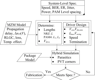
This dissertation focuses on high-speed circuit design for the integration of hybrid optoelectronic interconnects. It bridges the gap between electronic circuit design and optical device design by seamlessly incorporating the compact Verilog-A model for optical components into the SPICE-like simulation environment, such as the Cadence design tool.
Optical components fabricated in the IME 130nm SOI CMOS process are char-acterized. Corresponding compact Verilog-A models for Mach-Zehnder modulator (MZM) device are developed. With this approach, electro-optical co-design and hybrid simulation are made possible.
The developed optical models are used for analyzing the system-level specifications of an MZM based optoelectronic transceiver link. Link power budgets for NRZ, PAM-4 and PAM-8 signaling modulations are simulated at system-level. The optimal transmitter extinction ratio (ER) is derived based on the required receiver’s minimum optical modulation amplitude (OMA).
A limiting receiver is fabricated in the IBM 130 nm CMOS process. By side-by-side wire-bonding to a commercial high-speed InGaAs/InP PIN photodiode, we demonstrate that the hybrid optoelectronic limiting receiver can achieve the bit error rate (BER) of 10−12 with a -6.7 dBm sensitivity at 4 Gb/s.
A full-rate, 4-channel 29-1 length parallel PRBS is fabricated in the IBM 130 nm
ating at more than 10 Gb/s. Lessons learned from high-speed PCB design, dealing with signal integrity issue regarding to the PCB transmission line are summarized.
ACKNOWLEDGMENTS . . . v
ABSTRACT . . . vii
LIST OF TABLES . . . xiii
LIST OF FIGURES . . . xiv
LIST OF ABBREVIATIONS . . . xxii
1 Introduction . . . 1
1.1 Motivation . . . 3
1.2 Contributions . . . 4
1.3 Dissertation Organization . . . 4
2 MZM Device Characterization and Behavioral Modeling . . . 6
2.1 MZM Device Mechanism . . . 7
2.2 Modeling for MZM . . . 12
2.2.1 Grating Coulper . . . 12
2.2.2 Silicon Waveguide . . . 15
2.2.3 High-Speed Phase Modulator . . . 15
2.2.4 Low-Speed Phase Modulator . . . 19
2.2.4.1 Thermal Phase Modulator . . . 20
2.3 EO Co-Design Consideration . . . 21
2.3.1 Current-Mode Drive . . . 22
2.3.2 Voltage-Mode Drive . . . 27
2.3.3 Velocity Mismatch . . . 27
2.4 MZM Measurement and Behavioral Simulation . . . 31
2.5 Summary . . . 34
3 A Reconfigurable MZM Based Optical Link Budget Analysis . . . . 35
3.1 Derive OMA for Receiver . . . 36
3.2 Determine ER for Transmitter . . . 38
3.3 Correlation between Transmitter and Receiver . . . 45
3.4 Reconfigurable MZM Transmitter Simulation . . . 47
3.5 Summary . . . 48
4 A Hybrid Optoelectronic Limiting Receiver . . . 50
4.1 Receiver Architecture . . . 51
4.1.1 Photodiode and Trans-impedance Amplifier . . . 52
4.1.1.1 Gain and Bandwidth . . . 54
4.1.1.2 Noise and Sensitivity . . . 56
4.1.2 Limiting Amplifier . . . 59
4.1.2.1 Gain Stages with Active Feedback . . . 60
4.1.2.2 DC Offset Compensation . . . 62
4.1.2.3 Large-Signal in Limiting Region . . . 63
4.1.3 Output Buffer . . . 65
4.2 Experimental Results . . . 68
4.2.2 Bathtub and Sensitivity . . . 71
4.3 Summary . . . 73
5 A 10 GHz Phase Lock Loop Design . . . 78
5.1 PLL Architecture . . . 79
5.2 LC VCO Design . . . 80
5.3 Loop Stability Analysis . . . 83
5.4 Circuit Block Design . . . 86
5.4.1 Phase Frequency Detector . . . 86
5.4.2 Charge Pump and Passive Loop Filter . . . 87
5.4.3 Frequency Divider . . . 90
5.5 PLL Phase Noise Analysis . . . 92
5.5.1 Noise Sources and Noise Transfer Function . . . 93
5.5.2 Phase Noise Simulation . . . 94
5.6 Experimental Results . . . 96
5.7 Summary . . . 101
6 A 10 Gb/s Full-Rate 4-Channel 29 -1 Parallel PRBS . . . 102
6.1 PRBS Principles . . . 104
6.2 Transition Matrix Method and Correlation . . . 105
6.3 Circuits Design and Simulation . . . 108
6.3.1 Current Reference . . . 109
6.3.2 CML DFF . . . 110
6.3.3 Clock and Data Buffers . . . 112
6.3.4 PRBS Startup . . . 113
6.4 Experimental Results . . . 115
6.4.1 Packaging and Socket . . . 116
6.4.2 PCB Engineering . . . 117
6.5 Summary . . . 124
7 Conclusion . . . 125
REFERENCES . . . 128
APPENDIX A Verilog-A to Enable Optical Simulation . . . 135
APPENDIX B Determine the PRBS Feedback Tap . . . 139
APPENDIX C First Author Publications during 2013-2016 . . . 141
2.1 RLGC parameters at 10 GHz. . . 18
2.2 Parameter description used in Equation 2.9 and Equation 2.10, corre-sponding values used for curve fitting in Figure 2.10 are listed. . . 19
4.1 TIA design parameters . . . 54
4.2 Comparison of the optoelectronic RX fabricated in 130 nm (SOI) CMOS process. . . 74
5.1 Loop filter parameters when fV CO = 11 GHz, N = 128, b = 25.57, c = 9, P M = 65◦. . . 89
5.2 Simulated opppcres resistor and MIM capacitor characteristics at three corners in IBM8HP process. . . 89
5.3 Noise transfer functions from PLL o/p to each noise sources. . . 93
6.1 Comparison with recent PRBS generators published in JSSC. . . 103
6.2 QFN package electrical parasitic provided by the vendor. . . 116
6.3 Design parameters of single-ended and differential transmission lines made of RO4350B Rogers material. . . 120 6.4 Transient measurement for RF cable and three different transmission
lines with 500 mVP P PRBS-7 pattern at 10 and 15Gb/s, respectively. 121
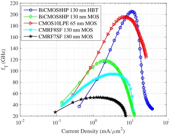
1.1 Simulated fT versus current density for four generations of IBM
pro-cesses. The width for HBT and MOS are 5µmand 15µm, respectively. Minimum length is used. . . 2
2.1 Illustration of a MZM device, HSPM cross-section, not drawn to scale. . 9 2.2 Optical power transmission characteristic of the MZM as a function
of the phase difference with and without considering the insertion loss introduced by the optical components. . . 10 2.3 Layout of a PAM4 MZM device. . . 11 2.4 Measured transmission spectrum characteristic of the MZM device
shown in Figure 2.3. . . 11 2.5 Fiber array alignment to grating couplers on the silicon photonic die
fabricated as a part of this research. . . 13 2.6 Loss profiles of IME TE 1550 nm grating coupler tested with 22◦
polished angle fiber array. . . 14 2.7 Decompose HSPM model into electronic model and photonic model. . . 17 2.8 The object properties of a Verilog-A HSPM cell. . . 17 2.9 Concatenate 1000 HSPM cells in Cadence schematic. . . 18 2.10 Simulated and measured results comparison of (a) the change of
rela-tive phase shift and (b) pn junction capacitance as a function of the reverse-biased voltage on a 5 mm long HSPM. . . 19
modulator (not drawn to scale). . . 20
2.12 DC characteristic of a 200 µm long thermal phase modulator. . . 21
2.13 Flowchart for the MZM-based transmitter design. . . 22
2.14 Schematic of the NRZ TX circuit to drive the MZM. . . 24
2.15 (a) CML dc transfer characteristic. (b) Vtail-input characteristic. . . 25
2.16 A segmented MZM device consists of fourteen lumped HSPM elements and PIN PM as dc phase device. . . 28
2.17 Illustration of the segmented MZM with lumped HSPM devices. Each segment has a dedicated push-pull driver. . . 29
2.18 Velocity mismatch simulation of NRZ and PAM-4 signaling at 32 G symbol rate (9.8 ps optical delay per segment). . . 30
2.19 Deterministic jitter of the ideal PAM-4 signal. . . 31
2.20 Eye pattern at 20 Gb/s with a 1 Vpp differential drive for a 5 mm MZM using a 1555 nm wavelength. (a) Compact model simulation result. (b) Measured result in [6]. . . 32
2.21 Prototype of a MZM device wire-bonded on PCB. Fiber array is aligned on top of the chip. . . 33
2.22 Eye pattern at 12.5 Gb/s with a 1.8 Vpp differential drive for a 1.1 mm segment MZM in Figure 2.3. (a) Compact model simulation result. (b) Measured result. . . 33
3.1 A conceptual MZM based hybrid silicon photoinic link block diagram. . 37
3.2 MZM based optical link specification parameters. . . 37
3.3 Inverter based optical front-end receiver. . . 38
FinFET CMOS process (in,rms = 4 µA, Vth = 20 mV, ZT IA = 58
dBΩ, ρ= 0.8 A/W). . . 39
3.5 Latch-based level shifter with example of potential reliability issue at the start of the signal toggling. Voltage at node 3 may jump to 2*VDDH or −VDDL so that will stress the gates of INV1 and INV2. . 40
3.6 A block diagram of the MZM segment driver. . . 41
3.7 Illustration of the reconfigurable MZM transmitter using segmented serpentine layout style for the proposed driver shown in Figure 3.6. . . 42
3.8 An example of the OE buffer from TSMC digital standard cell library. . 43
3.9 Optical power transfer function of the MZM in a 130nm SOI CMOS process with different lengths (an effective phase shift of 7.58◦/mm is extracted when operating at 32 Gb/s). . . 44
3.10 MZM ER and IL versus length. . . 45
3.11 OM AP D versus ER with varying input laser power. . . 46
3.12 The overload current seen from the TIA versus ER. . . 47
3.13 Simulated NRZ modulation format eye diagrams with 5 segments and 9 segments, respectively, operating at 32 Gb/s. . . 48
3.14 Simulated PAM4 modulation format eye diagrams with 5+9, 4+7, 3+5 segment combinations operating at 64 Gb/s. . . 49
4.1 The architecture of the proposed hybrid optoelectronic receiver. . . 52
4.2 Limiting receiver design specification partition. . . 53
4.3 The schematic of the the TIA with photodiode, triple-well NMOS is used for TIA core devices. . . 54
delay at nominal process corner, 40 C. . . 56 4.5 Histogram plot from nominal process Monte Carlo simulation of a 1.2
V nfet biased at maximumfT, 40◦C, in IBM 130 nm CMOS process. . 57
4.6 Post layout simulation eye diagram of TIA output at 4 Gb/s. . . 58 4.7 TIA input referred current noise spectrum from post layout simulation. 59 4.8 Bandwidth improvement factor and stage dc gain versus the number
of stages for an achievable gain-bandwidth product of 20 GHz (20×1
GHz). . . 61 4.9 Topology of the limiting amplifier. . . 62 4.10 Illustration of dc offset compensation. . . 64 4.11 Schematic of the folded cascode gain-boosted opamp used in the dc
offset compensation feedback loop. . . 65 4.12 A 2.5 GHz 150 mVP P sinusoidal signal gets amplified and gets more
NRZ-like waveform with edges sharpened, as it travels along the LA chain. . . 66 4.13 The schematic of the level shifted output buffer. . . 67 4.14 Post layout simulated eye diagram of the signal coming out from the
output buffer at 4 Gb/s. . . 68 4.15 (a) Chip microphotograph. (b) Chip-on-board bonding to the PCB.
(c) PCB setup. (d) Test setup in the Lab. . . 70 4.16 Block diagram of the test setup used for measuring the eye diagram
and BER of the designed receiver. . . 71
4 Gb/s with (a) 2 dBm and (c) 6dBm laser power, at 5 Gb/s with (b)
2.8 dBm and (d) 6 dBm laser power, wavelength is set at 1550 nm. . . . 72
4.18 (a)-(c) Electrical eye diagrams of a single-ended output of the limiting receiver measured with PRBS-31 from 4 Gb/s to 5 Gb/s. (d) Oscillo-scope mode at 5 Gb/s with PRBS-7 pattern. . . 75
4.19 Power consumption breakdown of the limiting receiver. . . 76
4.20 BER bathtub measurement of the limiting receiver with PRBS-31 operating from 4 Gb/s to 5 Gb/s. . . 76
4.21 Sensitivity plot of the limiting receiver with PRBS-31 operating from 4 Gb/s to 5 Gb/s, BER versus MZM OMA and average power. . . 77
5.1 Schematic of the proposed type-II third-order PLL architecture. . . 79
5.2 Schematic of the LC VCO. Control bits C < 2 : 0 > control the capacitor bank for discrete frequency coarse tuning, C0=66 fF. . . 81
5.3 Two different VCO layout examples. . . 82
5.4 Layout extracted simulation results of VCO characteristics. . . 83
5.5 PLL model with possible noise sources. . . 84
5.6 Plot of unity loop bandwidth over zero versus capacitor ratio in the loop filter for 65◦phase margin. . . 85
5.7 Schematic of the linear phase frequency detector. . . 87
5.8 State diagram of the linear phase frequency detector. . . 87
5.9 Schematic of charge pump. . . 88
5.10 Simulated MOS capacitor characteristics with vary gate voltages at three corners. . . 89
5.12 Schematic of CML divider-by-2. . . 91
5.13 Schematic of TSPC divider-by-2. . . 92
5.14 Plots of PLL noise transfer function for each noise source. . . 94
5.15 Phase noise of each noise sources introduced into the PLL. . . 95
5.16 PLL output noise due to individual noise sources. . . 96
5.17 A micro picture of the PLL. . . 97
5.18 Signal generator, signal analyzer and the prototype PCB. . . 98
5.19 VCO frequency versus capacitor control bits (66f F incremental) when the PLL is in the lock state. . . 99
5.20 PSD of (a) the reference clock at 83 M Hz and (b) a PLL/64 output signal at 166M Hz. . . 99
5.21 Phase noise of (a) the reference clock and (b) the PLL/64 signal. . . 100
5.22 Comparison of the measured and the simulated phase noises for PLL and free-running VCO. . . 101
6.1 System block diagram of the MZM based PAM-4 transmitter using the 4-channel parallel PRBS. . . 103
6.2 Ann-stage PRBS generator with possiblenandkcombinations (adapted from [74]). . . 104
6.3 Single-ended version block diagram of the full-rate 4-channel 29 −1 parallel PRBS. . . 107
6.4 Auto-correlation and cross-correlation of the 4-channel PRBS genera-tor (signal amplitude rescaled to -1 and 1). . . 108
cascode current mirror and BJT current mirror with beta helper and
emitter degeneration. . . 110
6.6 Schematic of the BJT DFF employed in Figure 6.3. . . 111
6.7 Schematic of the XOR-merged DFF employed in Figure 6.3. . . 111
6.8 Schematics of (left) clock buffer employed in Figure 6.3 and (right) bias condition for DFF clock inputs. . . 113
6.9 Schematic of output buffer. . . 113
6.10 PRBS start-up process by enabling “set” signal. . . 114
6.11 Simulated eye diagrams of data pattern at 40 G Baud rate for NRZ, PAM-4/8/16. . . 115
6.12 Micro photograph of half of the fabricated die. . . 116
6.13 Picture of the prototype FR4 PCB. . . 117
6.14 Eye diagrams of PRBS output with the prototype FR4 PCB. . . 118
6.15 Block diagram of the FFE to process the signal. . . 118
6.16 Transmission line sample board made of RO4350B material. Total length of the transmission line including SMA footprints is 1.368 inch. 119 6.17 Cross-section of single-ended microstrip, GCPW and differential GCPW transmission lines. . . 120
6.18 Measured S-parameters of the sample transmission lines in Figure 6.16. 121 6.19 TDR Simulated characteristic impedance with 25 ps rise time for a 10 M Hz to 20 GHz GCPW measured S-parameters . . . 122
6.20 Picture of the prototype Rogers PCB. . . 123
6.21 Eye diagrams of PRBS output with prototype Rogers PCB. . . 123
wire bonding (Bond wires drawn not to scale). . . 124
– ER Extinction Ratio
– FEC Feedforward Error Correction
– LA Limiting Amplifier
– LFSR Linear Feedback Shift Register
– MRM Micro Ring Modulator
– MZM Mach-Zehnder Modulator
– NRZ Non-Return-to-Zero
– OMA Optical Modulation Amplitude
– PAM Pulse Amplitude Modulation
– PLL Phase-Locked Loops
– PPG Pulse Pattern Generator
– PRBS Pseudo-Random Bit Sequence
– PVT Process, Voltage and Temperature
– TIA Trans-Impedance Amplifier
CHAPTER 1
INTRODUCTION
High-speed, low-power, small form factor interconnects are increasingly being demanded in today’s large-scale computing and switching system applications. For example, contemporary data centers can use 4-lane 25 Gb/s optical transceivers to achieve 100 Gb/s data transfer for different distances depending on the cable options. Ethernet and optical transport network (OTN) protocols have put 400G physical layer technology development on the agenda in several emerging industry standards, such as IEEE 802.3bs [1], ITU-T G.709 [2], MSA [3] and OIF [4], to upgrade from the 100G standard. Advanced modulation scheme such as the pulse amplitude modulation 4-level signaling (PAM-4) is adopted in the newer standard to achieve higher throughput in next-generation designs.
Electrical I/Os have reached a bottleneck in efficiently raising the speed of the data transfer up to more than 28 Gb/s per lane data communication. This is true even for an ultra-short reach, due to the speed limitations of the switching devices and the requirements of complex circuits and systems used for compensating the electrical channel loss and dispersion. Taking the actual bias condition and parasitics into consideration, the maximum achievable operating frequency of a reliable system is usually less than 1/10th to 1/20th of the device’s cutoff frequency fT. As shown
four generations of IBM processes are compared. As demonstrated in the plot, it is challenging to achieve>50 Gb/s/lane data transfer even using the IBM 130 nm SiGe BiCMOS process.
10-2 10-1 100 101 102
Current Density (mA/µm2)
20 40 60 80 100 120 140 160 180 200 220
f T
(GHz)
BiCMOS8HP 130 nm HBT BiCMOS8HP 130 nm MOS CMOS10LPE 65 nm MOS CMRF8SF 130 nm MOS CMRF7SF 180 nm MOS
Figure 1.1: SimulatedfT versus current density for four generations of IBM
processes. The width for HBT and MOS are 5 µmand 15µm, respectively.
Minimum length is used.
Gb/s/lane [5]. While the Mach-Zehnder Modulator (MZM) fabricated in a silicon photonic platform also in 130 nm SOI CMOS being driven by external test equipment can achieve up to 40 Gb/s [6]. Comparable high-speed electrical devices (MOS or HBT) are not available for integration on the same die in the commercial silicon photonic process platform, therefore designers have to rely on an advanced CMOS or BiCMOS process to design faster electrical circuitry, and then interface them with the photonic chip. Packaging challenges involved with bonding options for the electrical circuits die and silicon photonic die are critical to the overall signal integrity, as well as optical packaging for high volume production.
1.1
Motivation
descrip-tion language developed for behavioral modeling of analog circuits, is a good candidate for addressing this essential need [8]. There has been a general lack of such compact models for integrating silicon photonic devices with CMOS electronics. Lacking such models hinders EO co-design simulation and link budget analysis.
1.2
Contributions
This dissertation focuses on the design, analysis and hardware implementation of high-speed integrated circuits for optical interconnects. Specifically it addresses:
• How to bridge the gap between electrical circuit design and optical device design by creating compact optical device models using Verilog-A.
• Using systematic optical link power budget analysis, which can optimize the system-level specification for NRZ and PAM signaling format. This will be used to further guide the circuit-level design and energy-efficient optical system development.
• The design of high-speed circuit blocks for optical receivers and transmitters.
• A high frequency PCB design for maintaining signal integrity.
1.3
Dissertation Organization
compact behavioral modeling. Chapter 3 presents a MZM based link power budget analysis, and proposes a NRZ/PAM-4 reconfigurable optical transmitter based on voltage mode drivers with a segmented MZM device. Chapter 4 showcases a hybrid optoelectronic limiting receiver design by using the IBM 130 nm CMOS process and an InGaAs/InP PIN photodiode device. Chapter 5 and Chapter 6 detail a high-speed type-II third-order charge-pump PLL design and a full-rate, 4-channel 29−1 length
CHAPTER 2
MZM DEVICE CHARACTERIZATION AND
BEHAVIORAL MODELING
This chapter focuses on modeling of one type of electrooptic modulators, which is called Mach-Zehnder modulator (MZM) [6]. MZM is by far the most reliable indirect optical modulator in silicon photonic platform, although its footprint is large comparing to Micro-Ring modulator (MRM) [13]. Thus it requires relatively more power for modulator drivers. MZM device working mechanism will be explained in the first place followed by Verilog-A model developing for behavioral simulation. Driving options will be discussed based on lumped element modulator and traveling-wave modulator. The performance of NRZ and PAM-4 signaling method will be analyzed.
2.1
MZM Device Mechanism
distance away from the core device, to make sure there is no collision between the alignment and bondwire or the chip package. With the continuous-wave light source being split evenly into the two HSPM arms, when an electrical field forced by the reverse-biased voltage applied on each of the HSPM arms inducing a change in the carrier density, which, in turn induces a phase shift as the optical wave propagates in the arms. Depending on the relative E-field polarity applied on the HSPM arms, the two paths of lights interfere either constructively or destructively when they combine together at the output. The phase modulation is converted into intensity modulation at the combiner. Without considering the insertion loss of all optical components, the optical power transfer function (Topt) of the MZM can be derived as shown in
Equation 2.1 [14, 16]. Here Pin and Pout are the input laser power and MZM output
power, respectively. Here,φ1 andφ2are the absolute phases of the two arms (HSPM+
PIN PM). However, in reality every optical components will introduce insertion loss. For accurate modeling, all these non ideal effects need to be considered into the model. An accurate Topt expression is given in Equation 2.2 [17]. In this model,k is
the mismatch factor between the two arms which will deviate from 0.5 in practice. The two branches of optical power before entering the combiner are represented by
P1 and P2and represented by Equation 2.3 and 2.4 in dB scale, respectively. The
two most significant insertion losses are introduced by the grating coupler (ILGC)
and the HSPM (ILHSP M), respectively. Losses introduced by other optical elements
such as the Y-junctions (ILY−junc.), silicon waveguides (ILW G) and the low-speed
phase modulator also need to be included in the MZM model. What’s more, the insertion loss for phase modulators can be partitioned into static and dynamic parts.
Topt derived from models with and without considering insertion loss versus phase
different extinction ratio (ER) and average power which will impact the optical link analysis. Further, the dc phase operating point φdc should be set at the quadrature
bias point (90◦) to achieve symmetric modulation. This can be achieved by either using an extra length (about 100 µm) of waveguide or PIN phase modulator for one of the arms. In order to save power consumption, the asymmetry length waveguide and PIN phase modulator can be used together.
Thermal or p-i-nPM
Buried Oixde Substrate n n n++ p p p++ A A` Grating coupler P N A A` P N High-SpeedPM Un-doped waveguide
mim. gap required
Contact Contact
Figure 2.1: Illustration of a MZM device, HSPM cross-section, not drawn to scale.
Topt =
Pout Pin 2
= 1 +cos(φ1−φ2)
2 (2.1)
Topt=
P1k+P2(1−k) + 2
p
P1P2k(1−k)cos(φ1−φ2) Pin10
ILY−junc.+ILW G+ILGC 10
(2.2)
P2|dBm =Pin|dBm−ILGC −ILW G+ 10log10(1−k)−ILHSP M −ILLSP M (2.4)
60 70 80 90 100 110 120
φ1 - φ2 (°) 0
0.1 0.2 0.3 0.4 0.5 0.6 0.7 0.8
To
p
t
w/ insertion loss w/o insertion loss
Figure 2.2: Optical power transmission characteristic of the MZM as a
function of the phase difference with and without considering the insertion loss introduced by the optical components.
The MZM figure of merit, VπLπ in the units ofV-cm, is defined as the product of
the driver voltage height and the MZM length to cause a phase shift of π. This can be expressed in Equation 2.5. In which, ∆φM ZM is the actual phase shift due to the
driver voltage of Vdrv applied on a MZM device length of LM ZM.
VπLπ =
π
∆φM ZM
VdrvLM ZM (2.5)
Figure 2.3 demonstrates a layout of the PAM-4 traveling-wave MZM device. A 200
MZM transmission spectrum for symmetric MZM has similar characteristic to the asymmetric MZM in [18, 6, 19, 20], but has less voltage dependency. This is plotted in Figure 2.4. The free spectrum range (FSR) wavelength is about 6 nm.
Thermo heater
Grating coupler 1.9 mm
1.1 mm
Figure 2.3: Layout of a PAM4 MZM device.
Figure 2.4: Measured transmission spectrum characteristic of the MZM
2.2
Modeling for MZM
Verilog-A language is chosen for the model development for its advantage to do co-simulation with transistor-level circuitry in Cadence design tool platform. However, because Verilog-A doesn’t support complex numbers, the power intensity and phase are processed separately. In order to display the units for optical power (OptPower) and optical phase (OptPhase) in the unit of Watts and radians, respectively, their natures should be added explicitly as a Verilog-A discipline [21]. The optical discipline is given in Appendix A.1. With optical power and phase discipline and nature defined, an optical source block can be made as a general cell for converting the voltage to the optical power and optical phase units. The corresponding Verilog-A code is given in Appendix A.2. The MZM model shown in Figure 2.1 can be partitioned into four sub-blocks in silicon photonic process platform, they are grating coupler, un-doped waveguide used for optical routing and Y-junction, HSPM and PIN PM. Each optical components will be presented in the following.
2.2.1 Grating Coulper
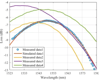
Grating couplers bring the optical signal into or out of the optical chip, typically externally interfacing to a fiber array as shown in Figure 2.5. The other interface of the grating coupler is in the plane of the wafer which connects to a 500 nm wide rib (fully etched) waveguide to the rest of the optical devices. There are two types of grating couplers which are single-polarization grating coupler (SPGC) and polarization-splitting grating coulpler (PSGC). As a rule of thumb, for IME TE SPGC aligned with the 22◦lid polish angle fiber array, the aligned fiber array is about 35µm
The loss profile in decibel scale can be expressed in Equation 2.6 with the parameters of peak loss (Losspeak), peak lambda (λpeak) and -3 dB wavelength (λ−3dB). Figure
2.6 shows four sets of SPGC measured data along with a Verilog-A model simulation result. The simulated result matches well with the measured result. The typical peak loss is measured about 4.5-6.5 dB per SPGC at different wavelengths depending on the different fiber array tilt angle and the actual height to die.
Loss=−Losspeak−
λ−λpeak
λ−3dB/ 2
√ 3
!2
(2.6)
Figure 2.5: Fiber array alignment to grating couplers on the silicon
Figure 2.6: Loss profiles of IME TE 1550 nm grating coupler tested with
2.2.2 Silicon Waveguide
Si waveguide in SOI technology has been made possible due to the high contrast between silicon and silicon dioxide. As optical signal routing, the waveguide intro-duces negligible insertion loss, but it does introduce phase shift and propagation delay which can’t be ignored in MZM design. Verilog-A compact model can capture the length and temperature dependent phase shift as shown in Equation 2.7, as well as insertion loss being customized for single-mode, multi-mode, different radius bends and tapers. In Equation 2.7,nSiis the Silicon’s effective refractive index and thef loor
function helps to remove the integer multiples of 2π. It also includes thermo-optic coefficient of the refractive index (ndT), which is about 1.86×10⁻⁴/◦C [22]. The
propagation delay is the waveguide length over the group velocity (vg) which can be
expressed in Equation 2.8. In which c and ng are the velocity of light in vacuum
and group index of silicon, respectively. For the purpose of simplicity and without losing accuracy, the refractive index and group index can be approximated to constant values for narrow range wavelength operation.
∆φ = 2π
(nSi−ndT ·(T −T0))L
λ −f loor
(nSi−ndT ·(T −T0))L λ
(2.7)
td=
L vg
= Lng
c (2.8)
2.2.3 High-Speed Phase Modulator
section of T-line or a distributed RLGC network in which the electrical propagation delay is designed to match the optical propagation delay. The latter is used here in which Rtl is a frequency-dependent metal skin resistance. It changes from 2.5
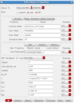
Ω/mm at very low frequencies up to 10 Ω/mm at 40 GHz. However, it is kept as a constant (e.g. 5 Ω/mm at 10 GHz ) in the model for simplicity and without losing accuracy at the same time. Moreover, the value shown in the component description format (CDF) parameter can be overwritten for other frequencies by editing the object properties of the symbol in Cadence, e.g., shown in Figure 2.8. Ltl andCtl are
the inductance and capacitance between the metal traces, respectively, which are also frequency-dependent [15]. The p-n diode can be modeled as parasitic resistance Rpn
and depletion capacitanceCpn. Cpncharacteristic varies with the applied reverse-bias
voltage as shown in Figure 2.10 [6]. The RLGC parameters used for the modeling at 10 GHz are listed in Table 2.1. A rough estimation of the microwave velocity (p 1
Ltl(Ctl+Cpn)) and optical group velocity (
3×10⁸m/s
ng ) are approximately 8.5×10
7m/s
and 7.5×10⁷m/s, respectively. We can observe that the two velocities are roughly
matched. Velocity mismatch effect will be analyzed in detail in later section. The distributed elements can be concatenated to form the MZM arm, the output phase of each stage reflects the voltage-dependent phase-change induced by the current stage, added to the phase of the next stage. The segment length of each cell should be set
< 101 n 3×10⁸m/s
g×5×fN yquist. e.g., for operating at 10 Gb/s, the segment length of the cell should
be at least less than 300 µm. Using small cell length will result in a large number of segments in cascade for a long MZM arm. However, there is a convenient way to do series connection as illustrated in Figure 2.9 for a thousand 3 µm cells to form a 3
L
tlR
tlC
tlElectronic Model
Optical Model
P
outФ
outΔФ
(V,L)
P
Loss(V,L)
P
inФin
V
td(L)
td(L)
Figure 2.7: Decompose HSPM model into electronic model and photonic model.
Figure 2.9: Concatenate 1000 HSPM cells in Cadence schematic.
Table 2.1: RLGC parameters at 10 GHz.
Rtl Ltl Rpn Ctl
5 Ω/mm 450 pH/mm 15 Ω·mm 123 f F/mm
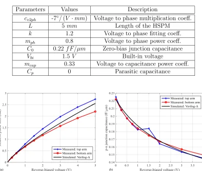
For the optical model, physical model equations for the voltage dependent dynamic phase shift and depletion junction capacitance are given in Equation 2.9 and Equation 2.10, respectively [8, 23]. The description of the parameters are detailed in Table 2.2. Simulated results using Verilog-A based on the physical models for relative phase shift and depletion junction capacitance for a 5 mm long HSPM are well matched with the measured results given in [6]. They are plotted in Figure 2.10(a) and (b), respectively. The HSPM has static insertion loss and dynamic insertion loss due to the doped waveguide and the applied modulation voltage. The static insertion loss is about 0.63 dB/mm which will contribute significant amount of loss when the device length is long. The scale of the dynamic insertion loss is 1/10 smaller of static insertion loss and will be decreased with increasing the applied voltage.
4φ=cV2P h·L·
π
180 ·(k·VR)
mph (2.9)
Cd=C0
1 + VR
Vbi
−mcap
Table 2.2: Parameter description used in Equation 2.9 and Equation 2.10, corresponding values used for curve fitting in Figure 2.10 are listed.
Parameters Values Description
cv2ph -7◦/(V ·mm) Voltage to phase multiplication coeff.
L 5 mm Length of the HSPM
k 1.2 Voltage to phase fitting coeff.
mph 0.8 Voltage to phase power coeff.
C0 0.22 f F/µm Zero-bias junction capacitance
Vbi 1.5 V Built-in voltage
mcap 0.33 Voltage to capacitance power coeff.
Cp 0 Parasitic capacitance
(a) (b)
Figure 2.10: Simulated and measured results comparison of (a) the change of relative phase shift and (b) pn junction capacitance as a function of the reverse-biased voltage on a 5 mm long HSPM.
2.2.4 Low-Speed Phase Modulator
less current to induce larger phase shift range is desirable for low power design.
Buried Oixde Substrate
p p++
p p Si
p++
Contact Contact
500 nm 800 nm
8 µm
Buried Oixde Substrate
STI p++
STI Si
p++
Contact Contact
500 nm 800 nm
8 µm
(a) Cross-section of thermal phase modulator. (b) Cross-section of p-i-n phase modulator.
Figure 2.11: Cross section of (a) thermal phase modulator and (b) p-i-n phase modulator (not drawn to scale).
2.2.4.1 Thermal Phase Modulator
The thermal phase modulator (TPM) is a doped Si waveguide as shown in Figure 2.11 (a). It relies on resistive heating to induce phase shift of a length of Si waveguide. The additional phase can be increased with input current as expressed in Equation 2.11. In whichηis the tuning efficiency in the units ofradians/mW. The measured dc characteristic of a 200µm long p-doped TPM which features a cross-section denoted in Figure 2.11 (a) is plotted in Figure 2.12. It can be observed that its resistance is not a monotonic relationship with respect to the power. The corresponding η is about 0.11 radians/mW. Using TPM for quadrature phase bias is not a low-power solution as it requires more current to achieve the phase shift when compared to the PIN PM.
Figure 2.12: DC characteristic of a 200µm long thermal phase modulator.
2.2.4.2 PIN Phase Modulator
The p-i-n phase modulator, as shown in Figure 2.11 (b), is used in forward-biased condition at carrier injection mode to create the change of refractive index. They are usually used to provide low-speed optical phase modulation, for instance control the quadrature dc phase bias point in MZM device. Like HSPM, it also has static insertion loss and dynamic insertion loss.
2.3
EO Co-Design Consideration
length thus is a preferred option for on-chip driver design, although mismatches in differential drive will introduce chirping effects. However, signal chirping techniques can be useful in long-haul optical transmission [24] which won’t be discussed here. A flowchart for the CMOS photonic design methodology is shown in Figure 3.2.
Figure 2.13: Flowchart for the MZM-based transmitter design.
2.3.1 Current-Mode Drive
As the operating frequency increases, the electrodes of the long MZM device should be treated as transmission line when the arm length has a physical dimension comparable to 1/10 of the signal wavelength. The wavelength (λ) can be calculated with Equation 2.12, in which,f andεef f are the operating frequency and the effective
λ = 3×10
8m/s
√
εef f ×f
(2.12)
Since MZM electrodes can be designed as on-chip transmission line according to the back-end of the process line metallization specification, current-mode driver is a natural fit to drive the traveling-wave MZM device at high-speed data rates. It is also required to provide enough voltage swing [25][26]. As an example, IBM 130 nm CMOS process which features a 1.2 V core device and 2.5 V I/O device, which maximum operating voltage is 1.6 V and 2.7 V, is employed for implementing the CML driver with 1.2 V single-ended swing as the schematic shown in Figure 2.14. For speed consideration, the differential pair (diff-pair) should use 1.2 V core devices. For reliability issue, 2.5 V I/O devices (M3a, M3b) have to be cascoded on 1.2 V devices as shown in Figure 2.14, at the sacrifice of speed. Transistor sizing, bias scheme, and parasitic introduced by the pad and bond wire are all critical design considerations for high-speed circuit design.
In order to efficiently use the bias current to obtain the desired voltage swing, the input pair (ML1,2 and MR1,2 in Figure 2.14) of the CML driver are operating
VDD14 Vcas Vbn Vbn Cb Rb Vb Optical Input VDD25 Rt RL M1a M1b Ms1 Ms2 M2a M2b M3a M3b RL Rt Optical Output 1.3~2.5V 24 mA Vdsat:200 mV Bond wire Bond wire model
P2 P1 V1p V1n Grating Coupler CML CML driver 11.4 mA 48µ/120n 100µ/120n 220µ/240n 70 50 200 µm
Radius = 12.5 µm
2.5 mm
Figure 2.14: Schematic of the NRZ TX circuit to drive the MZM.
The fall-time of the output is contributed by discharging the load capacitor during which the transistor transitions from sub-threshold region to saturation region (It will enter triode region until Vg > Vd+VT H when the amplitude is large), with the
discharge current reaching close to the tail current. Here, output slew-rate limitation is alleviated by using a large tail current. The slope in the region II can be increased by reducing the overdrive voltage of the input pair [27], this will also help to satisfy Equation 2.13 to maintain the tail current source in saturation, as is illustrated in Figure 2.15 (b).
Vpmin=Vcm−Vgs,MR,L|I
-1 -0.5 0 0.5 1 0.2 0.25 0.3 0.35 0.4
Vinp - Vinm (V)
V ta il ( V )
-1 -0.5 0 0.5 1 -1
-0.5 0 0.5 1
Vinp - Vinm (V)
V o u tp V o u tm ( V )
Figure 2.15: (a) CML dc transfer characteristic. (b) Vtail-input
character-istic.
Open-drain CML with single termination of 50 Ω at the far-end of the TWMZM is chosen for power saving purpose if the far-end can be perfectly matched. Indeed, this method can only be used for frequencies up to a few gigahertz since the matching at the far-end can hardly be made perfect [28]. Active back termination can be used to save power[29, 30]. A 2.5 mm long bondwire is adopted to introduce enough parasitic inductance for series peaking. However, the series peaking only works for open drain CML [31]. A headroom of 250 mV is chosen to satisfy theVdsatofM s. The size ofMs
desired 24 mA current capability, it would result in a relatively large size for the input pair and the cascoded devices M3. This is detrimental to high-speed performance. However, the size of M3 can’t be too small due to the ESD considerations. Thus, there is a trade-off between TX speed and ESD tolerance. Explicit capacitor is needed for the nodeVcas to minimize the signal feed-through due to the parasitic capacitance
of Cdg,M3.
Since the MZM driver consumes large current (24mA), the resulting diff-pair size is large, thus exhibiting large input capacitance. A predriver stage is therefore necessary [28] to drive the output stage with the required swing and suitably fast transitions. This requires the supply voltage of the predriver to be 1.4 V. Since the gate capacitance ofMR2 is about 33 fF and suppose theVoutp1node has 15 fF parasitic
capacitance, including the drain capacitance of MR1, it requires the load resistance RL to be smaller than 95 Ω to keep the rise-time less than 0.125 UI (unit interval).
Consequently, a 70 Ω load resistance with 11.4 mA tail current is chosen for the predriver. It also needs a minimum 0.4 V amplitude with a common-mode voltage of 1 V for the predriver diff-pair to be efficiently switched on and off. The size of the prominent n-channel MOSFETs and the resistor values are annotated in Figure 2.14.
It is worth noting that, in order to pass the lowest frequency component at certain data rate with certain length of the PRBS pattern, the on-chip ac coupling components Cb and Rb need to be chosen large enough [32]. DC coupling or use
2.3.2 Voltage-Mode Drive
Voltage-mode driver is suitable to drive lumped-element load. Circuit design tech-niques for voltage-mode driver are required to provide enough voltage swing as well as high-speed data rates [33][34]. For a lumped-element MZM device, inverter based drivers are the better option because it doesn’t consume static current dissipation and precludes the need of termination resistor for impedance matching. Shorter length MZM devices feature high VπLπ are highly desired for inverter based driver[35]. A
long MZM which consists of multiple HSPM segments arranged in serpentine style as shown in Figure 2.16. Each segment is 500 µm long that can be treated as a lumped-element. It can be configured as either NRZ or PAM-4 modulation by controlling the drivers. For this application, flip-chip or CuPillar bonding options feature extremely small parasitic inductance are necessary for the inverter based driver integration. Another main challenge for multiple segments lumped-element MZM transmitter design is precision delay cells between every two consecutive segments for velocity matching are required [36].
2.3.3 Velocity Mismatch
Pads location for LSB drivers
Pads Location for MSB drivers The length of the waveguide can be tuned to meet the delay cell design spec.
The difference of the large and small waveguide turns will be compensated by the turns for routing the next segment.
Large turn Small turn
Figure 2.16: A segmented MZM device consists of fourteen lumped HSPM elements and PIN PM as dc phase device.
schematic is illustrated in Figure 2.17. By varying the time delay of the delay cell with an offset time, defined by tos, with respect to the optical propagation delay. In
this example, the optical propagation delay is set to 9.8 ps. And the MZM device is modulated with 32 Gb/s electrical signal. As evident in the NRZ and PAM-4 eye diagrams, which are plotted in Fig. 2.18, by varyingtosfrom 0.5 ps to 2 ps, large delay
intrinsic deterministic jitter comparing to NRZ signaling. This can be observed from Figure 2.19. With a 10 ps 10%-90% rise and fall time 10 Gb/s bit rate, PAM-4 signal has 5.66 ps deterministic jitter due to the cross point of certain level transitions. In certain practical applications, forward-error-correction (FEC) with DSP techniques are required for PAM-4 signaling modulation due to more jitter and less SNR than NRZ signaling modulation [37].
vo ut h< 1> vout l< 1> vou thb < 1> vou tl b< 1> drvr drvr vou th < 2> vout l< 2> vou thb < 2> vou tl b< 2> delay drvr drvr vou th < 3> vout l< 3> vout hb < 3> vout lb < 3> delay drvr drvr vout h< *> vo ut l< *> vou thb < *> vou tl b< *> delay drvr drvr In Inb
Figure 2.17: Illustration of the segmented MZM with lumped HSPM
PAM-4 deterministic jitter
Figure 2.19: Deterministic jitter of the ideal PAM-4 signal.
2.4
MZM Measurement and Behavioral Simulation
Figure 2.20: Eye pattern at 20 Gb/s with a 1 Vpp differential drive for a 5 mm MZM using a 1555 nm wavelength. (a) Compact model simulation result. (b) Measured result in [6].
Figure 2.21: Prototype of a MZM device wire-bonded on PCB. Fiber array is aligned on top of the chip.
(a) Simulated (b) Measured
252.9 µW
Jitter p-p: 22 ps Avg Power: 203 µW Bit Rate: 12.5 Gb/s ER=2.19 dB
152.6 µW
2.5
Summary
A traveling-wave MZM device is fabricated and characterized. A library that consists of optical components behavioral models is created which enables the co-simulation of a silicon photonic MZM device and the CMOS transistors in Cadence Spectre. Current-mode and voltage-mode driver schemes with respect to multi-segment lumped-element and traveling-wave MZM devices are discussed. Velocity mismatch effect is emphasized with compact model behavioral simulation. The power consumption of voltage-mode driving scheme may comparable or even exceed the power consumption of current-mode driving scheme as the data rate getting higher and number of the lumped elements getting larger due to the CV2f relationship.
CHAPTER 3
A RECONFIGURABLE MZM BASED OPTICAL LINK
BUDGET ANALYSIS
Hybrid integration of CMOS chip with silicon photonic devices has emerged as a promising cost-effective solution to meet the ever increasing data transfer bandwidth requirement in the computing system. MZM device is by far the most reliable indirect optical modulator in silicon photonic platform, though its footprint is large and thus requires relatively more power for the drivers. Escalating the amplitude modulation scheme from NRZ (PAM-2) to PAM-4, even to increase the data rate to PAM-8 requires an analytic model to estimate the trade-off among the electrical-to-optical (EO) channel loss over the sacrificed signal-to-noise ratio, the circuit design complex-ity, the chip area and the power consumption. It is imperative to find a methodology to evaluate the link topology at the system-level and guide the transistor-level design of the transceiver circuits.
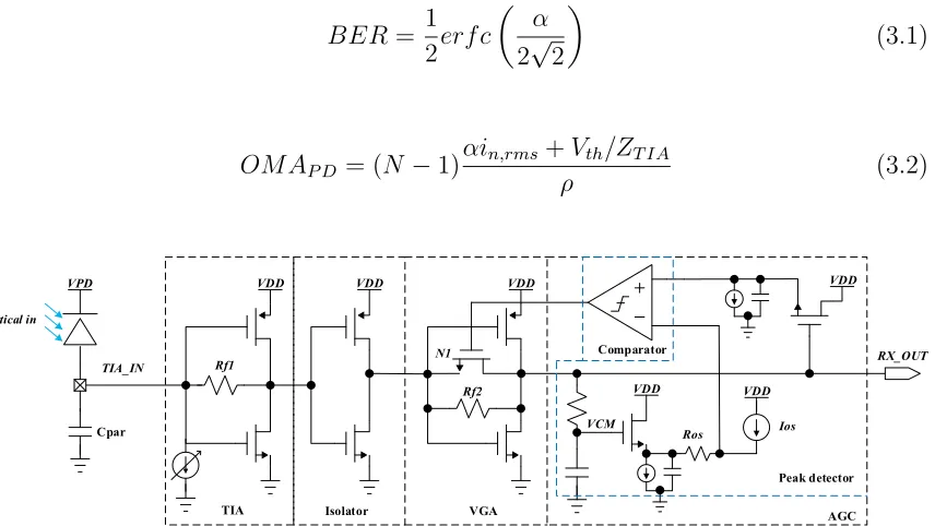
modulation with different extinction ratios (ER) can be achieved with the one design solution. Figure 3.1 illustrates a conceptual MZM-based silicon photonic link block diagram. The Germanium homo-junction photodetector (PD) is used at the receiver (RX) side features a small parasitic capacitor and thus can realize more than 25 GHz bandwidth with less than 2 V bias voltage, which has the best case responsivity (ρ) of 0.9 A/W. The ER[37] of the MZM at the transmitter (TX) side is determined by the MZM device insertion loss and modulation efficiency. The TX has to meet the minimum OMA requirement being derived at the RX side, considering the signal attenuation due to the PD coupling loss. However, the larger the received power at the PD, the more input current can be seen at the input of the transimpedance amplifier (TIA). Excessive amount of current will overload the TIA thus degrading its sensitivity. Therefore, an optimized optical link requires a suitable ER at the TX side to achieve the target BER performance with the least power consumption. Figure 3.2 lists the most important design parameters of interest for both transmitter and receiver. The electrical and optical parameters can be simulated and extracted from the process design kit (PDK) provided by the foundries which are essential for the detailed link analysis.
3.1
Derive OMA for Receiver
Ge PD TIA ER OMA Power CW laser SiPh MZM MZM driver CDR
Single mode fiber RF path
Figure 3.1: A conceptual MZM based hybrid silicon photoinic link block diagram. TIA RX Spec. PD MZM Laser TX Spec. Driver
Pave φdc
IL ER
VπLπ
BER
OMAMZM
Length Vswing
Speed
ρ
BW
OMAPD Vth
in,rms
ZTIA BW
ioverload
SNR Loss including
all the GCs
OMAMZM > min. OMAPD
λ
RIN Power
Figure 3.2: MZM based optical link specification parameters.
operating points between TIA and VGA, and provides small gain. The VGA makes the overall gain tunable to cover the cases of the input signal at different amplitude. This is achieved by using AGC to control the VGA stage.
The bit error rate (BER) performance is determined by the signal-to-noise ratio (SNR). It can be expressed with the complementary error function as given in Equa-tion 3.1 [40]. The SNR is represented by scaling factor α. The target α with other electrical parameters of the TIA set the OMA requirement seen by the PD as given in Equation 3.2. In which, N stands for N-level of PAM. in,rms is the TIA’s input
referred rms current noise. In this context, 4 µA in,rms is used as a design example.
Vth is the decision threshold after the TIA. ZT IA is the TIA’s transimpedance gain.
OM Amin is plotted in Figure 3.4. As shown in Figure 3.4, in order to achieve a BER
of 10−12, the approximate minimum OM AP D has to be larger than -10 dBm, -5 dBm
and -1.5 dBm for PAM-2, PAM-4 and PAM-8, respectively.
BER= 1 2erf c
α
2√2
(3.1)
OM AP D = (N −1)
αin,rms+Vth/ZT IA
ρ (3.2) VDD VDD RX_OUT TIA_IN VDD VDD VDD VDD VCM Ios Ros
TIA Isolator VGA AGC
Peak detector Comparator VPD Cpar Rf1 Rf2 N1 Optical in
Figure 3.3: Inverter based optical front-end receiver.
3.2
Determine ER for Transmitter
-11 -10 -9 -8 -7 -6 -5 -4 -3 -2 -1 0 OMA
PD (dBm)
10-15 10-14 10-13 10-12 10-11 10-10 10-9
BER
PAM-2 PAM-4 PAM-8
Figure 3.4: PAM-2/4/8 receiver sensitivity based on a 32 Gb/s TIA in
16nm FinFET CMOS process (in,rms = 4 µA, Vth= 20 mV, ZT IA = 58 dBΩ, ρ
= 0.8 A/W).
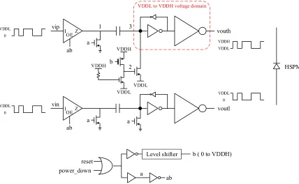
respective voltage domain when either one of the rst or pd signal is high. This is realized with an output enabled (OE) buffer. When the OE=1, the input can pass to Z. when OE=0, Z is in high impedance state so that a small pull down NMOS can pull the node to voltage low. The pull down NMOS is preferred to be sized small due to the high-speed operation. The VDDL to VDDH voltage domain pull down needs a level shifter circuit and a thick gate PMOS with an always-on weak pull down NMOS. When the reset or power down is high, b=0, node 2 is pre-charged to VDDH, so that node 3 is pull down to VDDL. When reset or power down is low, b=VDDH, node 2 is pulled to VDDL, so that node 3 is unaffected. The power down signal can cut off the signal path for a specific MZM segment even if the signal along the chain is presented.
1 3
C
INV1
INV2
1 3
0 VDDL
0 -VDDL 0
VDDL
VDDL 2*VDDH
-VDDL VDDH VDDH
2*VDDH
Reliability issue
Figure 3.5: Latch-based level shifter with example of potential reliability issue at the start of the signal toggling. Voltage at node 3 may jump to
2*VDDH or −VDDL so that will stress the gates of INV1 and INV2.
vip vouth ab voutl reset power_down Level shifter a
b ( 0 to VDDH) a a a b VDDH VDDL VDDL VDDH
VDDL to VDDH voltage domain
HSPM ab OEZ vin ab OEZ 1 2 3 0 VDDL 0 VDDL VDDL VDDH 0 VDDL I I
Figure 3.6: A block diagram of the MZM segment driver.
different ER can be achieved with disable or enable driving certain segments for the MZM device. The rms current for segment driver operating at 32 Gb/s can be 14 mA and 4.6 mA for VDDH (1.8 V) and VDDL (0.9 V), respectively. This added flexibilty can save power consumption by disabling drivers which are not necessary when the ER requirement is not high. It can also be configured as NRZ modulation if the patterns for serializer1 and serializer2 are kept the same.
ER, which correlates the OMA with the average power, is an important specifica-tion for optical modulators. The optical power transfer funcspecifica-tion (Topt) of the MZM
device is given in Equation 3.3 and is plotted in Figure 3.9 with different lengths. In this plot, the MZM is driven by a push-pull driver with 1.8 VP P swing on both of
the MZM arms. The dc phase difference (φdc) being introduced by the PIN phase
Pad location for LSB drivers
Pad location for MSB drivers
p-i-n phase modulator High-speed phase modulator Silicon waveguide
Figure 3.7: Illustration of the reconfigurable MZM transmitter using
segmented serpentine layout style for the proposed driver shown in Figure 3.6.
quadrature operation point for the best symmetric linear modulation. However, this assumption is started without considering the mismatches between the two arms due to process variation. φ1 and φ2 are the absolute phases of MZM’s two arms. k, which
deviates from 0.5, is the mismatch factor of the Y-junction and between the two arms. A total static insertion loss is expressed in Equation 3.4. The two branches of optical power before entering the combiner is represented by Equation 3.5 and Equation 3.6, respectively. A dB scale is used in the above equations. The two most significant insertion losses,ILGC and ILHSP M,sat, are introduced by the grating coupler and the
high-speed phase modulators (HSPM), respectively. A nominalILGC of 5 dB is used
OE
I
Z
Figure 3.8: An example of the OE buffer from TSMC digital standard
cell library.
and -0.08 dB/mm, respectively, when it is reverse-biased at 1.8 V. The longer the HSPM, the more static insertion loss will be introduced. The larger the reverse-bias voltage is, the less the dynamic loss of HSPM is. The static and dynamic insertion loss, ILP IN,static and ILP IN,dyn, for a 250 µm PIN PM are 0.22 dB and 1.7 dB/π,
respectively. Moreover, losses introduced by other optical elements including the Y-junctions used for splitting and combing the lights, optical routing like the straight and turned silicon waveguides and the PIN phase modulators, are considered in the MZM model. Thus, the ER can be accurately derived from the plottedTopt in Figure
Topt=
P1k+P2(1−k) + 2
p
P1P2k(1−k)cos(φ1−φ2) Plaser10
ILY−junc.+ILW G+ILGC 10
(3.3)
ILstatic=ILGC +ILW G+ILHSP M,static +ILP IN,static (3.4)
P1 =Plaser−ILstatic+ 10log10k−ILHSP M,dyn(φ1)−ILP IN,dynφdc (3.5)
P2 =Plaser−ILstatic+ 10log10(1−k)−ILHSP M,dyn(φ2) (3.6)
30 40 50 60 70 80 90 100 110 120 130 140 150
φ
1 - φ2 (°)
0 0.01 0.02 0.03 0.04 0.05
T o
p
t
L = 1mm L = 2mm L = 3mm L = 4mm L = 5mm L = 6mm L = 7mm
0.5 1 1.5 2 2.5 3 3.5 4 4.5 5 5.5 6 6.5 7 7.5
MZM Length (mm) 1 2 3 4 5 6 7 8 9 10 11 12 13 14 15 16 17 18 ER (dB) 9.5 10 10.5 11 11.5 12 12.5 13 13.5 14 14.5 15 IL (dB)
ER @ dc ER @ 32 Gb/s Optical IL
Figure 3.10: MZM ER and IL versus length.
3.3
Correlation between Transmitter and Receiver
The OMA after the coupling at the RX PD side needs to be guaranteed to meet the BER requirement for PAM-N signaling. This is plotted in Figure 3.11 with the laser power ranging from 10 to 19 dBm (numbers in red are denoted at the side of each curve). The dash-dotted horizontal lines are the minimum required OMA at the PD for PAM-N signaling derived from the parameters used in Figure 3.4. 5 dB insertion loss is assumed per grating coupler. It can be observed that there is an optimal ER for this specific MZM device, which is around 8 dB. In order to meet the OM Amin for PAM-4 and PAM-8 RX sensitivity requirement, laser power needs
ER but doesn’t necessarily help the OMA . This is because longer MZM device can introduce excessive loss.
10 11 12 13 14 15 16 17 18 19
PAM-4 PAM-8
PAM-2
Laser (dBm)
Figure 3.11: OM AP D versus ER with varying input laser power.
Laser (dBm)
Figure 3.12: The overload current seen from the TIA versus ER.
3.4
Reconfigurable MZM Transmitter Simulation
NRZ modulation format can be realized by completely powering down either all the 5 LSB segments or the 9 MSB segments. The simulated results are shown in Figure 3.13. Since NRZ modulation requires less ER specification, segments within LSB or MSB can be further powered down to save power consumption. With 10 dBm (10 mW) laser power and a fixed current setting for p-i-n phase modulator. The obtained ERs are about 2.94 dB and 5.55 dB, respectively. The driver power consumption is 290 mW and 522 mW, respectively.
shown in Figure 3.14. In order to meet the receiver’s sensitivity requirement, PAM-4 signaling need more laser power. Here as a example, given 13 dBm (19.95 mW) laser power and a fixed current setting for p-i-n phase modulator. The driver power consumption for achieving 9.38 dB, 7.12 dB, 4.92 dB extinction ratio is 812 mW, 638 mW and 464 mW, respectively. Different ER specifications for PAM-4 modulation format can be realized to meet different application scenarios. The middle eye height is smaller than the height of the top and bottom eyes for the 3+5 segments combination. This can be improved by tuning the dc phase point by changing the current setting for the p-i-n phase modulator.
5 segments 9 segments
ER 2.94 dB ER 5.55 dB
Figure 3.13: Simulated NRZ modulation format eye diagrams with 5
segments and 9 segments, respectively, operating at 32 Gb/s.
3.5
Summary
5+9 segments 4+7 segments 3+5 segments
ER 9.38 dB ER 7.12 dB ER 4.92 dB
Figure 3.14: Simulated PAM4 modulation format eye diagrams with 5+9, 4+7, 3+5 segment combinations operating at 64 Gb/s.
CHAPTER 4
A HYBRID OPTOELECTRONIC LIMITING RECEIVER
consideration and speed limitations of the transistors in available silicon photonic process [5, 46, 38, 47].
Design analysis of the fabricated limiting receiver is elaborated in section 4.1. System-level analysis and discussion with measurement results are given in section 4.2. Finally, key design considerations learned from this case study are summarized.
4.1
Receiver Architecture
In this work, a limiting receiver was designed in IBM 130 nm CMOS process. Similar to prior work such as [46, 43], without having CDR or DeMUX circuitry, the signal is taken out by using an output buffer. As illustrated in Figure 4.1, the signal path of the CMOS limiting receiver consists of a front-end trans-impedance amplifier (TIA) followed by limiting amplifier (LA) stages, with a high gain feedback opamp for dc offset compensation (DCOC). The final outputs will be level shifted by a output buffer (OB), which utilizes a 3.3 V power supply. A pair of off-chip capacitor (Cex)
is used to achieve the desired low-frequency cut-off for this DCOC loop. The CMOS chip also includes a bandgap reference (designed using 3.3 V transistors) and bias generator. A top illuminated InGaAs/InP PIN photodiode (PD) is side-by-side wire bonded to the TIA input on the CMOS die.
The system specification of the limiting receiver is illustrated in Figure 4.2. The overall bandwidth (BWtot) of gain stages in cascade in the linear region can be first
order estimated by using BW12 tot =
1
BW2
1
+BW1 2 2
Cex TIA
InGaAs/InP photodiode VPD
LA Stages OB
Opamp SMF
CMOS Chip Boundary Bandgap & Bias Generator
VDDL VDDH
VDDL
Bondpad with bondwire
Linear region Limiting region
Figure 4.1: The architecture of the proposed hybrid optoelectronic re-ceiver.
to meet 2/3 of the data rate (B) for optimal inter-symbol interference (ISI), noise and power trade-off [28]. Using the first order equation in the linear region mentioned before as an example, it can be derived that the bandwidth of TIA and LA can be set at about 0.9×B and 1×B, or 0.7×B and 2×B, respectively. In this work, the performance of the limiting receiver is studied with a TIA bandwidth less than 0.5×B and a LA bandwidth about 2×B in the limiting region.
4.1.1 Photodiode and Trans-impedance Amplifier
BW
Responsivity (ρ) Dark current
Linear region Limiting region
PD TIA LA OB
Signal integrity ESD
Electro-migration TX Spec.
ER
Laser Pave Wavelength
Couple loss Limiting RX Spec. BER
OMA (Sensitivity) Pave (Overload current)
Gain
Power BW
Gain BW
Noise Power
Figure 4.2: Limiting receiver design specification partition.
a shunt feedback common source stage and a second stage with a biased n-channel transistor (nfet) which act as an active inductor load for bandwidth extension. The second stage also provides additional gain and adjusts the dc operating point for the next block by adjusting the bias voltage (Vb),Vb must be set belowVDDL+Vthto keep
M3 in saturation. The input current level will be raised when the incoming optical
intensity is increased, this can result in improper dc operating point for the next stage, which is CML type in the LA stages. This undesired current is called overload current which can be canceled by turning on the overload control signal (ol−en).
tia_out
V
bR
F2M
1M
2M
3R
BCgs
R
LVDDL
V
PDR
F1ol_en
L
sL
gL
pOptical in
Input pad
PD pad
Figure 4.3: The schematic of the the TIA with photodiode, triple-well NMOS is used for TIA core devices.
Table 4.1: TIA design parameters
PDK displayed resistance (Ω) Total width of nfets
RF1,2 RL RB M1,2 M3
384 768 4.6 K 20.4 µ 4.8 µ
4.1.1.1 Gain and Bandwidth
The first stage TIA gain frequency response is expressed in Equation 4.1 without taking the bondwire effect into account. The low-frequency trans-impedance gain is approximately RF as long as gmRF, gmRL 1. The dominant pole is due to
the input capacitance including the PD junction capacitance, PD pad, TIA input device and pad capacitances. The corresponding input resistance is expressed in Equation 4.2. The second pole is resulted from the TIA’s first stage output resistance (RL k gm1M1) and the capacitance associated at that node, which will be much smaller
domain.
RT(f) =
RL(1−gmRF)
1 +gmRL
1
1 + pf
1 1 +
f p2
(4.1)
Rin=Zin(s)|s=0=
RL+RF
1 +gmM1RL
(4.2)
With the design parameters listed in Table 4.1, the post layout simulation results for gain frequency response of the 2-stage TIA is plotted in Figure 4.4. The layout parasitic is critical, as an example here, it reduces the TIA’s bandwidth by more than half when compared to the schematic simulation result. Even though thefT,max mean
value of the nfet is 117.8 GHz, from the schematic Monte Carlo simulation as plotted in Figure 4.5. The achievable gain-bandwidth product using the nfet in practical design will be much less thanfT,max, especially without using on-chip inductors. This
is due to the actual bias condition and parasitic effects introduced at the input and output nodes of the nfet.
G
ro
up
d
el
ay
(
ps
)
TI
A
g
ai
n
(d
B
Ω
)
Frequency (GHz )
Figure 4.4: Post layout simulation results for TIA frequency response and
group delay at nominal process corner, 40◦C.
this simulated group delay variation has 330 ps, which is 1.32× UI for 4 Gb/s. The effect of group delay distortion on the TIA output eye diagram is not obvious due to the jitter is overwhelmed by the source jitter. Moreover, the signal will enter limiting region in the following LA stages, thus making the group delay specification less critical at this stage.
4.1.1.2 Noise and Sensitivity
The first stage in the front-end circuit is key to the noise performance. The input-referred current noise density at the middle band frequency is derived in Equation 4.3. There,γ is a process dependent thermal noise coefficient of the nfet. The thermal noise due to the feedback resistor (RF) is directly reflected at the input. It’s preferable
to increase RF andgm ofM1 (equivalent to gain) to reduce the noise floor. However,
90 100 110 120 130 140 150 f
T,max (GHz)
0 20 40 60 80 100 120 140
No. of Samples
Number = 1000 Mean = 117.82 GHz Std Dev = 8.88 GHz Biased at 2.78 mA/µm2
Figure 4.5: Histogram plot from nominal process Monte Carlo simulation
of a 1.2 V nfet biased at maximum fT, 40◦C, in IBM 130 nm CMOS
process.
referred to the input will start to increase from the TIA bandwidth onwards. This can be observed from the post layout simulation result as plotted in Figure 4.7. For integrated noise, it is necessary to look at the whole spectrum up to about twice the TIA bandwidth[48]. The estimated input referred rms current noise (in,rms) is less
than 1.2 µA.
I2n,in ≈ 4kT
RF
+ 4kT (1−gmRF)2
1
RL
+γgm
(4.3)