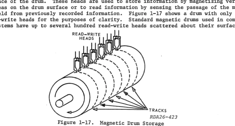
Technical. Training
STUDENT TEXT
E'3ABR30534E 000'
KDA3032
ELECTRONIC COMPUTER AND SWITCHING SYSTEMS SPECIALIST
Cql1PUTER UNITS AND COM-TRAN1.0.
JUNE 1981
USAF
TECIINICA~
TRAINING ·SCHOOL
3,390th Technical Training, Group
. Keesler
AirF orce
Base,Missis~ippi
- - - -... --~ .. '" Designed Fo~ATC CO:l1rse Use --~~I~ ..
CON TEN T S
TITLE
Ghapter I - Computer Units and Programming ••••••••••••••••••••••••••••••.•.•.•••••• Computer Units and Data Flow ••••••••••.•••••••.••••.••••••••..•••••••••••••••• Data Flow ••.•••.••••••••••••.••••••••••...••••••••.•••••••••••••••••••••.. Data Flow Summary . . . . Review Questions 1-1 ••.••••••••••••••••••••••••••••••••.•••.•••••••••••••••.•• Memory Units •..••••••.•••••••.••••••••••••.••••••••••••••••.•••••.•••... , ..•• Mode of Access ••••••••..•••••••.••••••••• ; •••••••.••••••••...••.••••...•• -t" Access Time ••••••••.••••••••••••••.••.••••.•••..••••••• ' ••••••••••••••••••• Capacity •••••..•••••••••••••••..••.•••••••.•••.••.•••••••••••••••••••• ' •..• Permanence ••.•••..•••••••••.••••••••••.••.•••••••••••••••••.•••••.•...•••. Volatility ••••.••••••••••••••..••••••••....••.•••...••••.•••.••••••••••••. Storage Devices •••••••••••••••••••.•••.•••••••••••••.••.•.••••••••.••••••••••• Magnetic Storage Sys terns •••••.••••••••••.•••••••••.•••..••••••••.•••••.••••••• Hysteresis Loop ••..•••..••••.•••••.•••••••••..•••.••••.•....•..••.•••••.•. F err i te Core Memory ••••••...•••••..•••••••••••••.••••..••.•..••.•••••••••• Magnetic Drum Memory •••.••••••••••••.••••••••••••...•.•.••••••..••.•.•.•.• Magnetic Tape Memory •.•••.•••••••••••••.•••.••••.•••..•.•...•...•..•. Review Questions 1-2 •••••••••.•.•••.•••••.••.••••••..••••... ~ ••...••••••••.• Terminal ,Equipment ••.•••.••••..•.•.•••.• ' .••••.•••••.•••••.•....••....•••.••••• Card Reader ..•.•••.••••.•••••.••.• ~ •.•.•••.••••...•••.•.•••..•••••••••.• Card Punch ••••••••.••.••.•••..••.•••.••••.•••.••••••••••....•••..•••.••••. Line Printer •.•.•.•••••••...•••..••••.••••.••••••.•••.••••.•••.••••.•••.•• Tape Drive Unit ••••..•.••.•...•..•..••.•.••••••••..•••••.••••.••••••.•••.• F1exowriter . . . ; •.••••• Display Equipment ••.•••••••.•••.••.•••••••••••••••••••.••••••••••••••••..• Review Questions 1-3 •••••••••••••.•••••••••.•..••••..•.••.•••..••••••..••...•• Computer Operation and Familiarization ••••••.•.••••..•••••••••..•••..•••.•.••• Individualism of the COM-TRAN TEN Computer System •.•••... ' .•...••.•...••. Operating the Computer •••••••••••••••• : ..•.••.•.••...••• , ••.•..••••••.••..•.... Controls and Switches ••..•••....•..•••••••••.•••••••••.••••••••••••••••• ' •• Computer Registers and Display Panel •.•••••••••••••••..•.•••.•••.•••••. ' ••• Hexadecimal Review ••.••.•....••.•...•••.•••....••..••••..••••..••••.•.•••. Manual Input' Procedure ...••..•••....•••.••••.•...••.•••..•.••••••••.•.•• ," Manual Output Procedure •.••••..••••..••....••••..••....••••••••••••••••••• Review Ques tions 1-4 .•.•••••••••••.•••••••••••.••••••••••••••••••..•.••••••••• Progrannning ••••..••••••• ' •••.•••••..•••••••••••.••••.••.•••••.••••....•.••••••. Type of Instruction •••••••••.••...•••••.••••...•••.••..•••••.••••••.•••••• Ins truc tion Repertoire •.••••••••••••••.••••...•••.•.•..••.•••••••.•••.•••• Instruction Format •••••.•••.••••••••••••.•.••••••.•••••....•...•.•••... , Addressing Upper Memory .••••.•.•••..•••...•••••. , •••••..•••••.•••••..•.••. Indexing .•.••..•••••••••••.••••••••••...•••..••. ; •...••.••••.•••..•••••••• Number Representation ••••••••.•••.•••••.•••••••••.•••••••••••..•••••...••. Instructions •...•••...•••••.•.•..••••..••••.•.•...•.••.••••.••.•.••••••• Review Questions 1-5 •..••..•..•.•••••••••••••••.•••••••••••.••••.•••.••.•.•••. Review Questions 1-6 •••...••...••••••..•••••.••••.•••••.•••••.•.•••••...•• Review Questions 1-7 •••.•.•••..•••.•••••..•.•••••••••.•.•••••.••••....•....••. Review Questions 1-8 •••••••••...•••...•.•••••••.•••••••••••••••.••..•••••.•••. Review Ques tions 1-9 ..•••••••••.••.••.••••••••..•••..•••••••••.•.•••••••.••••. Procedures for Writing Programs ••••.••..•••••••.•.•••.••••••.••••...•••.•..••. Programming Problem ••••••••••..••.•••••••••••.•.••.•.••••••••••••••••••••••••• Alphabetical Sunnnary of Instructions ••••••..•••.•.••••.•..••••.•.•..•••...•.•• Numerical Sunnnary of Instructions ••••••.••••••.••••.••••••••••••••••••..•••••• Computer Terms Glossary •.•.•••••..••••.••.••.••.•••••.••.•••.•.••••.•.•..•.••• Supersedes KDA-3032, June 1977
Chapter II - Computer Units Logic Analysis •.•••.•••••••••••••••••••••••••••••••••• Special Components •••••••••••••••••••••••••••••••••••••••••••••••••••••••••••• Phantom OR-Gate •••.••••••••••••••••••••••••••••••••••••••••••••••••••••••• NOR-Gate Latch ••••••••••••••••••••••. ·0 • • • • • • • • • • • • • • • • • • • • • • • • • • • • • • • • • • • •
D-Type Flip-Flop; •••••••••••••••••••••••••• " ••.••••••••••••••••••••••••••• Single Shot (SN74l2l) ••••••••••••••••••••••••.•••••••••••••••••••••.•••••• Positive AND-Driver· •••••••••••••••••••••••••••••.••••••••••••••••••••••••• Special Component Sutmnary •••••••••••••••••••••••••••••.••••••••••••.••••..•••• Review Ques tions 2-1 ..••••.•• , •.•••••••.•••••••••••.•.•••••••..••••••••••••••• Compu ter Uni ts ••••••••••••••••••••••••••• ' •••••• '.' ••••••••••••••••••••••.•••••• Key to Logic Diagrams •••..••••••.••••••••••••••.•..•••••••.••••••••• ; ••••• Review Ques tions 2- 2 .•.••.•.••••••••.•••••••••••••••.••••••••••••••••••.••.••• Clock .••••••••••••••.••..••.••••..••.•••••••••.•.••••••••••••.••••••••.•.••• Review Questions 2-3 ••••••.•••••••••••••••••••••••• " .••••••••••.•••••••••••.••• D-Register ••.••••••••••• , •••• , •••••••••••• " ., .• , ••••• , ••.•• " •••••• , , •• , • Review Questions 2-4 ••••••• ,., ••••••• , •••••• ,., ••• , •• "." •.• ,., ••••• , •. , •••.• Input Register ••••••••••••••••••..••••••••••••••••••..•••••..•••..•••••.•• Review Questions 2-5 ••••••••••••••.••••.••••••••••• ; •••••••••••••••••••• A • • • • .
-B-Regis ter ••.•••..••••••••••••••••••••••••••••••••••••••••• ' .•••.••.•.•.••• Review Questions 2-6 •••.•••.••.•••••••••••••••••••. ' ••••.••.•• ' ••.••••..•••••••• Memory Module. ~' ••• '.' .••.•.••••••••••••••••••••••• ': •.••••••••••••••••••••.. Review Ques tions 2~ 7 •••.••..••••••.••••.••••.•••••••••••••••••••••••••••...• M-Regis ter •••••.•••••••••••••••.•. " ••.••••.•••••••••••••••••..•••..•••••. Review Questions 2-8 •••••••••••.••••••••••••••••••••••••••••••••••.•.••••••••• X-Register ••••••••••••••••••••.••••••••••••••••••.•••••••••.••••••••••..•• Review Questions 2-9 .••••••••••••••••••••••••••• ; ••••••••••••••••••••••••••• ,. P-Register •••••••••••••••••••••••••••••••••••.•.••• , .••.•••.•••••.••••. 0 • • • • •
Review Ques tions2-l0 •••••••••••••••••••••••••••••• 0 • • • • • • • 0 • • • • • • • • 0 • • • • • • • • •
A-Register (Accumulator) ... , ••••••••• 0 • • • • • • • • • • • • • • • • • • • • • • • • •
Review Ques tions 2-11 •••••••••••••••••••••••••••.•••••••••••••••••.•••••••••.• ALU Module •••••••••.•••• 0 • ~ • • • • • • • 0 · • • • ; • • • • • • • • • • • • • • • • • • • • • • • • • • • • • • • • • • •
Review Ques tions 2-12 •••• 0 • • • • • • • • • • • • • • • • • • • • • • • • • " • • • • • • • • • • • • • • • • • • • • • • • • • •
Q-Register •••••••••••••••••••• , •••••••••.••.•.•.••••••••••.•••••.•••••...••• Review Ques tions 2-13 •••••••••••••••••.•••••••••••••••••••..••••••.•. ' .••••••••• C-Regis ter •. ' •••••••.•••.••.•••••••••••••••••••.••••••••••••••• ~ ••••••••••.. Review Questions 2-14 •..••••.••••••••• , ••••••••••••••••.••••.••••••••••••••••• S-Register ••.•••••••••••••.••••••••••.•••••••••••••••• 0 • • • • • • • • • • • • • • • • • • •
Review Ques tions 2-15., •••••••••• ~ . . . . Program Instruction Logic Analysis •••••••••.•••••••••••••••.•••••••..•..••••••
Logic Timing Supplement •.•.•••..•••..••.•••••••.•.•••.•••••.•••••••••••••.. Acquisition Phase and DPA Pulses ••••• ~ •••••••.• : •••.•..•••.•.•.•••..••..•••• Review Questions 2-16 •••••••••• , ••••••••••••••. ,: •••••••.• ; •• : ••••.•••••....••••• Execution Phase ••.•••••••••.••••••••••••.•• ' ••••••••••••••••.•••••• ' ••••••••• Review Ques tions 2-17 ••••••••••••••••• · •••••••••••••••••••••• ; ••••.••••• ; ••••••
Chapter III -. Computer System Maintenance ... ' ••.••• ' •..••••••••••••• , .•.•••.••••••• '.' Computer Diagnos tic Programs ••••••••••••••••••••.••••.•••••••.•••••••••••••..• Purpose of Diagnostic Programs . . . . Basic Requirements ••••••••••••••••••••••••••.••••••••••.••...••••••••.•••• Review Ques tions 3-1 •••••••••.•••••••••••••.••••••••••••• · •••• , ••••.••••..••••••. Computer System TroubleshQoting •••••••• ; . . . .
Troublesnooting Techniques ••••••••••••••••••.••••••••• , ' .• , ••.•••••••..•••. Troubleshooting Example One ••••• · •••• , ••••••••••.•••••••••.•••••••••••••••• Review Questions 3~2 ••••••••••••••••••••••••••••••••••••••••.• ' ••••••...•.•• , •• Troubleshooting Example Two .•• o· ••••••••••• , •••• , , • , ••• , , , • , •.••• ,,' •••••• , ••
i i PAGE 125 125 125 126 128 129 130 l32 134 137 137 138 138 144 144 148 148 150 150 152 153 154 155 158 158 160 160 162 162 164 164 166 166 167 168 170 170 172 172 173 173 176 178 226 230 230
230\
232 233 235 235PAGE
Review Questions 3-3...
264
Chapter Review...
266
Signal Name Glossary...
269
CHAPTER 1
COMPUTER UNITS AND PROGRAMMING
In past blocks you learned numbering systems and computer circuits. These are all put together to look at the computer as a whole. You will not be separating the com-puter into the circuits, but into functional parts. You will learn how to operate the COM-TRAN TEN trainer and how to make the computer do what you want. You will learn to
program the COM-TRAN TEN. A computer can only do what it is told. Now start with the
basic computer block diagram.
COMPUTER UNITS AND DATA FLOW
Figure 1-1 is a block diagram of a basic computer. It is made up of 5 blocks. Each
block has a distinct function. All digital computers are made of these five basic blocks. Different computers can use different combinations of computer circuits to do
each 'of. these five functions. Refer to figure 1-1.
• INPUT - The Input Unit of a computer accepts information in various forms and con-verts it to a form which can be used by other units of the computer.
• OUTPUT - The Output Unit accepts information from the computer and sends it to' the output devices. These outputs can be in a form readable by man or in a form for the computer to use later.
• MEMORY - The Memory Unit stores information until it is needed by the computer. Memory locations are addressed so the machine can find the right information when it needs it, much like you would use a house address to find the right house. The most commonly used memory is magnetic core. It is a fast memory and will retain-any information that it has in case of a power failure.
INPUT DEVICES
--.
INPUTder Reader Card Reader
Teletypewriter Paper Tape Rea Magnetic Tape Magnetic Drum Display Input Optical Reader
Keyboards
Disk
OUTPUT DEVICES
Card Punch Line Printer Teletypewri ter Paper Punch Magnetic Tape Magnetic Drum CRT Displays Plotter Disk
.-,...
OUTPUTFigure 1-1
MEMORY
I--CONTROL
..
ARITHMETIC
• ARITHMETIC - Arithmetic Unit performs all arithmetic and logical operations. Arithmetic units usually do nothing more than add and shift. To multiply, it does a series of adds and shifts •
• CONTROL - The Control Unit generates all the signals at the proper time tO'do what needs to be done. It controls all the other computer units.
Data Flow
Before tracing the flow of data among'the five units of a computer, it is necessary, to understand the definition of the following terms:
1. Computer Word
2. Machine Cycle
3. Program Time
r(&S',
4. Operate Time
- A group of binary bits, handled by the computer as a single unit. Commonly referred to as the content of a memory .--±eea·t;i.-On-,
- The length of time which is required to acquire an instruc-tion from memory, decode the instrucinstruc-tion and execute it. '
- (Acquisition Time) The portion of a machine cycle when the
instruction is read from memory, de~oded, and prepared for
execution.
- (Execution Time) The portion of a machine cycle when the
instruction is actually performed.
5. Instruction Word - A computer word having two partw; instruction code (Op-Code)
and data address (Operand). The Op-Code tells the machine
what to do and the Operand tells, the machine where and with what data to do i.t.
6. Data Word
7. Program
- A computer word containing information or arithmetic value to be used in computations.
- A series of instruction words in logical order to solve a given problem.
With an understanding of these terms we can now discuss computer operation and data
flow. Computer words, both instructiori words and data words, are entered into the
com-puter's Input unit by some external device. The Input unit puts these words into
binary or some other' numbering system format that is recognizable by the computer. The
Input unit then transfers these computer words to the Memory unit for storage. The instruction words would be stored in logical order to form a program that would 'control the operations to be performed.
The Memory unit, now containing all instructions and data, can be used to output arithmetic and logical operations to the Arithmetic unit and receive the results of those operations from the Arithmetic unit. Those results can then be sent to the Output unit where they are put into a, format recognized by the external output device.
Of course, all operations of the machine and the sequence of all data transfers are controlled by the Control unit. The instruction words are transferred to the Control unit from the Memory. unit. The Control unit decodes these instructions into commands. The Control unit, operating under a timed sequence, causes a series of events to execute any command that it decodes.
Data Flow Summary
Information comes into the computer through the Input unit. This Input is controlled
by the Control unit. The information is put into Memory. The Control unit works with
the Memory unit and the Arithmetic unit to solve whatever problem you have told it to do.
When the computer gets the answer, it will put it in Memory. Then, the Control unit will
control the output of the answer through the Output unit. All of this is controlled by you up to a point. You tell the computer where to get information and what to do with it. You will learn how to do this later in the block.
REVIEW QUESTIONS 1-1
BASIC DIGITAL COMPUTER BLOCK DIAGRAM
Objective
Given a block diagram of a basic computer and a list of units and functions, label the units, match the functions to the units and trace data flow between the units.
A
D
RDA26-419
Figure 1-2
1. Analyze the basic computer block diagram (figure 1-2) and- list the name of each
unit to correspond with the label in the appropriate block.
a. b.
c. d.
e.
2. Using the following list, match the basic computer unit with its applicable
functional descriptions.
a. Input b. Output c. Memory
d. Control e. Arithmetic
______ Stores information until it is needed.
______ Performs all arithmetic operations.
Generates signals needed to do the work.
_______ Performs logical operations.
_______ Accepts information from the computer and sends it to an output device.
______ Works with all other parts of the computer.
3. Draw all the necessary lines to properly connect the units below.
Arithmetic
4. Give the function of each of the following: RDA26-420
Input-
Output-
Control-
Arithmetic-
Memory-MEMORY UNITS
The difference between a memory unit and a memory (or storage) device is an impor-tant distinction. Any device which is capable of holding binary information for a period of time may be correctly called a storage device. A memory unit, on the other hand, is a complete unit composed of many storage devices and the associated circuitry which con-trols and operates the unit. A memory unit may be used as the memory element (central memory) of a computer system or as an auxiliary storage unit for either the input
ele-ment or output eleele-ment (or both eleele-ments). The most common memory devices used are
magnetic cores, magnetic tapes, magnetic disk, magnetic drum, punched cards, and punched tape.
Only the central memory is used for all operations going on inside the computer. If
additional data, or even a specialized program, is required, then access is made to large blocks of data in an auxiliary memory are transferred to main memory in a single
opera-tion. If main memory fills up its available storage space with intermediate results or
output data, then a large block of data may be sent to auxiliary memory from the main
memory. Such transfers between the central memory and an auxiliary memory are called
I/O operations.
I/O operations are started by the computer through program contrul. After starting the transfer operation, some computers continue with their original task while the I/O
operation continues. I/O transfers may be from the input element to the memory element,
from the memory element to the output element. or from the central memory to an auxiliary memory which serves both the input and ootpot elements.
To understand the reasons why some storage units are used as central memory and other storage units are used as auxiliary. you must be able to define and use the following terms as they apply to memories: mode of access. access time. capacity. permanence. volatility. and computer word.
Mode of Access
Any memory unit that stores more than one item of information must have some system to identify and select a particular item for use by some other part of the computer. Normally. each separate item of data is stored in a separate "location" in the memory unit. and each location has a specific address. It is common prac.tice to number storage locations serially in octal notation. The method used to gain access to a specific loca-tion in a storage unit (central or auxiliary) is referred to as ';mode of access." There
are two major modes of access: random and sequential.
RANDOM ACCESS. A random access memory system is one in which any location in the
storage unit is equally easy to use; it takes the same amount of time to address any specific location in memory and use the data stored there. Any addressing scheme which is independent of previous addresses or that can address locations out of sequence is usually a random access system. Random access memories provide fast access to any par-ticular item of information stored in them. and they normally have a fixed access time.
SEQUENTIAL ACCESS. A sequential access memory system is one in which access to
memory locations occurs in series. The system must check all addresses between the present memory location and the desired location before the desired location can be used. In a sequential address system. the access time will vary depending on how many
loca-tions must be "passed through" before the needed location is found. Sequential access
memories are further broken down into two groups: cyclic and progressive.
Sequential Cyclic. The sequential cyclic mode is a mode of access in which each lOCation occurs in series and is available at a given fixed interval. Sequential cyclic memories normally have some rotating storage device so that the sequence of addresses and time until the needed location reappears is permanent.
Sequential Progressive. The sequential progressive mode is a mode of access in which each location occurs in series. but the system may move from location to location by the shortest route. A sequential progressive system does not move constantly in one direc-tion as does the sequential cyclic mode; rather. it may "search" in either direcdirec-tion to locate the desired memory location. The time required to find a given address in a sequential progressive system varies depending on the distance from the starting point to .the needed address.
Access Time
'gCAt
Access time is measured from the time information is requested to the time that
information becomes available. It is the time which determines the speed of the memory
system. In most applicatio~s. it is desirable to have as short an access time as
pos-sible. The central memory of a computer will always have a short access time; however. any auxiliary memories used in the system may have a relatively longer access time if they provide some other desirable feature.
access time is given in maximum, minimum, and average times. For example, in a sequen-tial cyclic mode, if the desired' location is close to the starting point, the access time will be very short; if the desired location was passed just before the request was made,
then the system must wait almost a complete cycle before the information"is available. The average access time for a sequential system is the mean time between the-minimum and maximum access times.
Capacity
The capacity of storage may be given in terms of binary bits, characters, or com-puter words that can be stored. Storage devices of small capacity, such as flip-flop registers, are usually rated according to their bit capacity. When describing the storage capacity of large devices, such as magnetic tapes or drums, the "word" capacity rather than "bit" capacity is usually given. In such cases the number of bits in a word must be stated if a useful comparison is to be made between different storage units.
Access time and capacity are the two most important characteristics of any memory system. They are determined by the type of storage device used. No one memory unit, in current production, combines the desired capability of large capacity and short access time. In fact, it will be found that most large capacity storage units have a long access time; most low capacity units have a fast access time. Therefore, a combination of stor-age units is usually used in a computer system.
Permanence
Permanence is the characteristic which determines whether the data in a memory unit may be erased. A magnetic memory is erasable since any selected "word" can be changed or altered without physically changing the memory unit or any of its parts. Some storage devices, however, are not erasable; that is, the stored data cannot be changed without physically replacing the storage device. For example, to alter the information stored in punched cards, new cards must be punched and used as replacements for the old cards.
Volatility
If information is lost when power is removed from a storage unit, the memory system is said to be volatile. A flip-flop register is volatile; a punch card "deck" is non-volatile. If a computer system uses a volatile storage system, positive steps must be
taken to preserve the stored information if it is not available elsewhere in .the system. Therefore, valuable information is normally stored in a non-volatile unit and put into
volatile storage only when it is to be operated on. In this way, critical data is
pre-served in the event there is .a power fault. Ferrite cores are non-volatile.
Since both data (information) words and instruction words are stored in memory and are not distinguishable in form from one another, some means is needed to separate instructions 'from data.'- This can be done by restricting instructions (the program) to the area of memory or by allowing access to memory on 'a sharing basis. In a time-sharing system, memory words accessed by specific timing pulses are automatically assumed to be instructions. The time in which an instruction is transferred to the control element from memory' is called the acquisition time. Acquisition time is then followed
immediately by execution time in which the instruction is obeyed. If a memory word is
accessed during execution time, it is automatically assumed to be data. A sequence of acquisition-execution time is called a machine cycle.
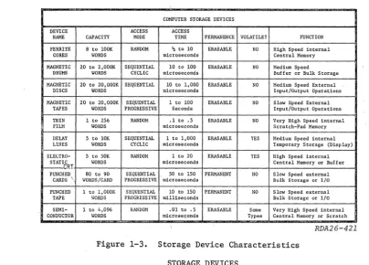
COMPUTER STORAGE DEVICES DEVICE ACCESS ACCESS
NAME CAPACITY MODE TIME PERMANENCE VOLATILE? FUNCTION FERRITE 8 to lOOK RANDOM l; to 10 ERASABLI\ NO High Speed internal
CORES WORDS microseconds Central Memory MAGNETIC 20 to 2,OOOK SEQUENTIAL 10 to 100 ERASABLE NO Medium Speed
ORUMS WORDS CYCLIC microseconds Buffer or Bulk Storage MAGNETIC 20 to 20, OOOK SEQUENTIAL 10 to 1, 000 ERASABLE NO Medium Speed External
DISCS WORDS microseconds Input/Output Operations MAGNETIC 20 to 20, aOOK SEQUENTIAL 1 to 100 ERASABLE NO S low Speed External
TAPES WORDS PROGRESSIVE Seconds Input/Output Operations THIN 1 to 256 RANDOM .1 to .5 ERASABLE NO Very Higb Speed inte.rnal
FILM IIORDS microseconds Scratch-Pad Memory DELAY 5 to 10K SEQUENTIAL 1 to 1,000 ERASABLE YES Medium Speed internal LINES IIORDS CYCLIC microseconds Temporary Storage (Display) ELEGTRO- 5 to SDK RANDOM 1 to 20 ERASABLE YES High Speed internal
STATIC WORDS microseconds Central Memory or Buffer
I---CRT
Slow Speed external PUNCHED 80 to 90 SEQUENTIAL 50 to 150 PERMANENT NO
CARDS \ WORDS/CARD PROGRESSIVE microseconds Bulk Storage or I/O
PUNCHED 1 to l,OOOK SEQUENTIAL 10 to 150 PERMANENT NO Slow Speed external TAPE WORDS PROGRESS IVE milliseconds Bulk Storage or I/O SEMI- 1 to 4,096 RANDOM .01 to .5 ERASABLE Some Very High Speed internal CONDUCTOR WORDS microseconds Types Central Memory or Scratch
RDA26-421
Figure 1-3. Storage Device Characteristics
STORAGE DEVICES
There are many storage devices available for use in computer systems. Some hElVe
been popular in the past and are now almost forgotten; others have been--and will
con-tinue to be--used in almost every computer system made. Some new storage devices have
been invented but have not yet found theic way into operational computer systems. Figure 1-3 provides information on the characteristics of many of the storage devices used in USAF computer systems.
MAGNETIC STORAGE SYSTEHS
Ferromagnetic materials make many excellent binary storage devices for use in com-puters. The "polarity" (N-S direction) of a magnetic field can represent a one or zero. This fact, coupled with the close relationship between electric current and magnetism,
is the reason ferromagnetic materials are used so often as compute~storage devices. In
fact, magnetic storage systems are the most common way of storing large amounts of com-puter data.
Magnetic storage systems may use tiny cores (doughnuts) of magnetic material, long strips (tapes) of magnetic material, rotating drums coated with magnetic materials, or
rotating discs coated with magnetic materials. In many cases, the actual area needed
to store one binary bit is as small as the head of a pin. This means that quite a lot of
information can be stored in a small area. For example: a 5-i~ch cube of magnetic cores
can store 150,000 bits of computer data; a standard 2,400-foot reel of 1/2 inch wide computer tape can hold over 2 million bits of computer data.
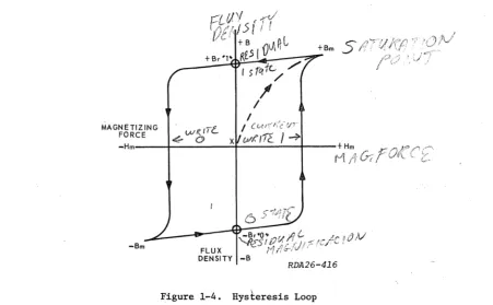
Hysteresis Loop
All magnetic storage systems utilize a physical phenomenon known as residual
mag-netism. Resi~ual magnetism means that a piece of ferromagnetic material will keep a giver
[image:11.549.65.469.63.352.2]bit of binary data as a magnetic field. This phenomenon can be shown on a graph of magnetic flux density (B) versus magnetizing force (H). This graph is called a B-H curve and, for ferromagnetic materials, becomes a hysteresis loop. A thorough and com-plete understanding of the hysteresis loop, or curve, will help you to maintain ferrite core memories, tape storage units, magnetic drums, and magnetic discs. In addition, knowledge of the hysteresis loop will assist your career progression when you are faced with SKTs. (Skill Knowledge Tests).
Figure 1-4 plots the values of flux density (strength and direction of magnetiza-tion) "B" versus magnetizing force "H" applied to a magnetic material. We can start our examination of the curve by locating point "X" in the center of the loop. This point represents the material in a neutral or unmagnetized condition. If a magnetizing force with a value of +Hm is then applied to the material, its flux density and direction will
be forced to point +Bm. Fortunately, with most magnetic materials, any increase in the
magnetizing force above +Hm will not increase the flux density above +Bm. When the
material is at point +Bm, it is said to be saturated; its flux density in one direction is maximum and cannot increase. This fact will cause the hysteresis curve to become a
loop. If the magnetizing force (+Hm) is now removed, the flux density of the material
will drop only slightly to point +Br (residual magnetism). This slight drop, instead of
the large drop common to most metals, is due to the high retentivity of ferromagnetic materials. Point +Br now represents a stable flux density and direction that can be called a binary one or zero, according to its application.
/
J'
I
,,-MAGNETIZING , (u.,-("./: tjT
W(ITe..
FORCE .ef.- 0 xiJWt'I1l.. /-;.
-Hm'---+---~----+_--~Hm •. I"__:
-J::-OI(CC'
nj1V{! . '
<r--RDA26-416
Figure 1-4. Hysteresis Loop
If we now desire to store the opposite binary number in the magnetic material, it is necessary to apply a magnetizing force of -Hm (equal in magnitude to +Hm but opposite in
direction). The application of force -Hm will cause the flux density to swiftly de9Tease
to zero and then move on to a maximum negative value, point -Bm. Again, if a force
greater than -Hm is applied, the flux density cannot become greater than -Bm. The
material has now become saturated with a magnetic flux density equal to +Bm but in the opposite direction. Once the force has been removed, the material will stabilize with
[image:12.541.52.503.308.587.2]its residual magnetism at point -Br. If point +Br was assigned to a value of binary one, then point -Br would be a binary zero.
The application of a force of +Hm to the magnetic material at the -Br point will cause it to switch to the +Bm point. Notice that this completes the hysteresis loop and completely bypasses point x. The only way to return the magnetic material to its unmag-neti.zed condition is to apply an AC sine wave decreasing to 0 volts. An examination of the hysteresis loop will reveal that, in normal operation, ferromagnetic material will remain at either point +Br (one state) or -Br (zero state). The application of magne-tizing force is required to make magnetic material change states (switch from one state to another).
In some applications of magnetic storage materials, the material will be moved rapidly under a small coil; this movement of magnetic ,fields past a coil will induce a current flow in the coil. The direction of current flow will indicate the direction of magnetization of the material, and the magnetic field will not be changed in any way. The data stored as two different directions of magnetic fields may be "read" over and over again. This type of nondestructive readout is often used for magnetic drums, mag-netic tapes, and magmag-netic discs. Of course, if it is desired to change the stored infor-mation, the use of the coil must be changed. To write on drums, tapes, or discs, the coil is connected to a current source; current flow through the coil produces a magnetizing force that can be used to store data in magnetic material.
One other form of magnetic storage device is a small core of ferromagnetic material that has several small wires passing through it. A single bit of information may be stored in or read from a single core. These cores are quite small, perhaps 15 to 50 thousandths of an inch in outer diameter. To produce a useful computer memory device, several thousand cores and their wires are placed in a frame (plane) about 6 inches square by 1/2 inch thick. These planes can be stacked together to make a memory array that will hold anywhere from 150,000 to 2 million bits of,computer data.
Ferrite Core Memory
A ferrite core memory ca~not be move~ past a coil to sense the state of the cores;
therefore, other electronic systems must be used to read out data from ferrite core arrays. Unfortunately, most of these systems involve destructive readout of the data stored in the cores. Destructive readout of ferrite cores takes advantage of the fact that the collapse of a magnetic field that surrounds a wire will induce current flow into the wire. Core memories are physically small and simp1e--compared to the motors and other mechanical parts needed with drums, tapes, and discs--but they have complicated electronic circuits needed to control the writing into, reading from, and restoring of
data into the cores. Not all "core" memories consist of individual cores·that are .
threaded by wires and assembled into planes. Some memory systems use ferrite plates with a series of holes through which the wires needed to read and write data pass. The plate is so constructed that each of the areas around the holes acts as a single core. The ferrite plate has characteristics similar to a plane of ferrite cores.
COINCIDENT CURRENT ADDRESSING. In order to use a ferrite core, the computer must be
able to write information into any given core and also to read information from any given core. The techniques used for writing into or reading from a selected core or group of cores (a computer word) are called address selection techniques. The address selection technique that this SG explains is one of a number of techniques that are available to manufacturers of ferrite core memories. The technique explained is the "coincident current technique" and is the most cOlllIllon1y used system of getting data into or from a magrietic core.
The basic concept of the coincident current selection technique is that two wires
states. This magnetizing force is in the form of current passing through a pair of wires. (Current flow through a wire sets up a magnetic field around the wire, which is directly proportional in strength to the current flow through the wire.) A combined current which
produces a magnetizing force of
±Hm
on the hysteresis curve is called a full-selectcur-rent. Each wire carries a "half-select" current; that is, a current with a magnitude of
H/2. If, and only if, a core receives the effect of a "full-select" current will it
com-pletely change states. This means that a wire carrying a half-select current can be threaded through many cores, but the only core affected by this half-select current will be the one core that is receiving an additional half-select current from another .wire that is also threaded through many unaffected cores.
After the ferrite core is completely saturated in one direction and the magnetizing currents removed, the retained flux will be almost that of saturation, and the direction of magnetization can be considered the one state. If and when the half-select currents are reversed to magnetize the core in the opposite direction, then the core will be con-sidered to be in the zero state. In the coincident current addressing technique, each half-select drive current applied to the wires is of such a value that each current alone does not provide enough magnetizing force to "switch" the core or cause it to reverse flux direction. However, with both half-select drive currents applied, there is
suffi-cient magnetizing force to cause t~e core to switch and retain, through its residual
magnetism, the new condition after the drive currents are removed.
Assume that the cores are designed to switch when approximately 0.350 ampere drive-current (±Hm) is felt by the core. Each drive line carries approximately 0.250 ampere. Either of the drive lines alone does not carry a sufficient current (magnetizing forcer-to switch the core. However, a combination of the two drive currents (0.25 ampere
+
0.25 ampere) will exceed the required switching value and cause the core to switch,providing that it is not already in the desired state.
+B
+Bm
-I
,,/"7
}/
/
/
MAGNETIZING /
FORCE X /
-Hm---+---~~~--~~~~--~t_---+Hm
-H!2 -H!2 +H!2! +H!2
-
/
-Br'·O ....-Bm FLUX
DENSITY -B
RDA26-417
Figure 1-5. Detailed Hysteresis Loop
The operation of the coincident current addressing technique can best be explained by
a more detailed study of the hysteresis loop of a ferrite core. (Refer to figure l-5.)
In the initial application of selection drive currents to the core, consider the core to be demagnetized (point "x"). As positive half-select drive currents are applied, mag-netization will take place. One half-select current will not be enough to saturate the core and place it at point +Bm; however, an additional half-select current will saturate
the core and place it at point +Bm. As the drive currents fall from maximum positive to
zero, the core's retentivity will allow only a slight drop in its flux density. When the drive currents fall to zero, the flux will remain stable at point +Br. At this time the core is in the one state.
If the core is stable at point +Br and a negative pulse of current is then applied
to both half-select drive lines simultaneously, the core will switch to point -Bm. As
the drive currents decay, the core flux density will come to rest at point -Br, and the core will remain in the zero state. The important thing to notice is that if the core is in a residual state (fEr) and only a single half-select drive current (H/2}.is applied and removed, the state of the core will not be changed. The square shape of the hysteresis loop shows that a certain current or magnetizing force must be applied to a ferrite core to cause it to change states. If less than a minimum force is felt by the ferrite core, it will remain in its pfeviously established stable state.
FLUX DI RECTION
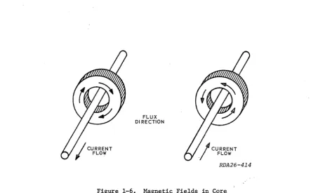
Figure 1-6. Magnetic Fields in Core
X AND Y SELECTION LINES. To understand how drive current flowing in wires threaded
through a ferrite core can produce one and zero states in the core, refer to figure 1-6. This illustration shows that current flow into the page would produce cores with a counterclockwise magnetic field. Current flow out of the page (toward you) would pro-duce cores with a clockwise magnetic field. These fields are in agreement with the ','left hand rule" which was mentioned briefly when you studied the basics of magnetism in the electronic principles course. One direction of the core's magnetic field is assigned
~he value of binary one and the opposite direction of magnetic field is assigned the value
[image:15.543.42.495.264.538.2]RDA26-415
Figure 1-7. Core Address Lines
Most of the ferrite cores used to store computer data do not have a single wire
applying magnetizing force to the cores. Instead they use two wires, each carrying a
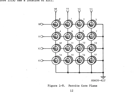
half-select drive current. For convenience, these address selection lines are usually called the X (horizontal) and Y (vertical) address lines. Figure 1-7 shows a single core threaded by X and Y address selection lines. Of course, each X line and each Y line passes through several other cores. Figure 1-8 shows a typical ferrite core plane with its X and Y selection lines.
The ferrite core plane in figure 1-8 contains 16 cores number 0 through 17 (octal). Each core is threaded by two address selection drive lines; each wire will carry a half-select current. Only the core that receives a magnetizing force from two wires (coinci-dent X and Y currents) will be selected. Each core has its own unique pair of X and Y lines that will make it become a selected core. It is standard practice to label cores by ,their X-Y address. For example, core 11(8) would be identified as address X2Yl; core 11(8) has a location of X2Yl.
yg Y1 Y2 Y3
X 1 >----H~ TA--H&i VJ-+il.H YJ--Hd-J V}--"
X2 >--+-I'lM-l In--HIi<+-I Vj~-tH-I V,HHI<-H
X 3 > - - t - f j r l - i VJ--H~ YJ-+fIrH Y}--HlH-!
RDA26-412
Figure 1-8. Ferrite Core Plane
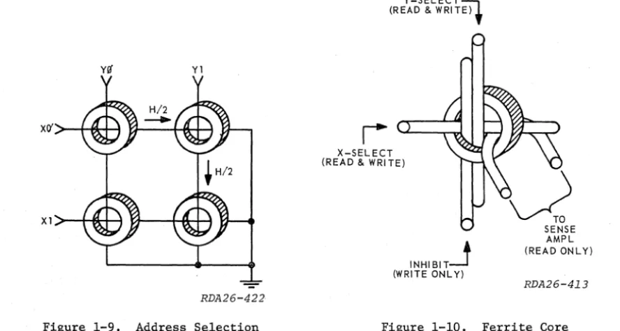
[image:16.546.42.494.394.693.2]Figure 1-9 shows four cores arranged in a very simple plane. Each core is threaded
with two lines, X and Y. Assume that all cores are in the zero state and we want to
write a one into core X0Yl. If a full select current with a value of +Hm is applied to
the x0 line, then both cores X0Y0 and X0Yl will be switched to the one state. If a full-select current of value +Hm is applied to the Yl line, then both cores X0Yl and XlYl will be affected. This is not quite what we want to do.
yff Yl
RDA26-422
Figure 1-9. Address Selection
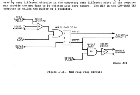
I
Y-SELECT-;;\l (READ & WRITE).
X-SELECT (READ & WRITE)
INHIBIT-1 (WRITE ONL Y)
SENSE AMPL (READ ONLY)
[image:17.547.44.488.170.407.2]RDA26-413
Figure 1-10. Ferrite Core
If, however, half-select currents of +H/2 are applied to the x0 and Yl lines at the same time, then only core X0Yl will receive the effect of a full-select current (+Hm). Each of the other cores along the x0 and Yl lines will receive only a half-select cur-rent. Therefore, only core X0Yl will be switched to the one state, and the other three cores in the plane will remain in the zero state. Two cores (X0Y0 and XlYl) receive half-select current, which is not enough to cause them to switch, and one core (XlY0) receives no current at all. Anyone of the four cores in this sample plane may be selected by pulsing the correct combination of X and Y lines with simultaneous half-select currents.
INHIBIT WINDING. Notice that the selection of a Gore that was in the zero state by
positive half-select currents caused it to switch to the one state. The application of negative half-select currents to a core can be used to switch it from the one to the zero state. However, sometimes we need to select a core but leave the state of that core un-changed. This need to select, but not change, usually is the result of wanting to "write a zero." "Writing a zero" requires that we add another wire to the simple core plane, an inhibit winding. The inhibit winding will carry currenc that opposes one of the positive half-select currents and prevents the address selec.ted core from switching to the one state. Since only one core from a plane can be selected at anyone time, a Single inhibit winding can be threaded through all the cores on a plane and· energized
only when it is necessary to"write a zero" into the selected core. In figure 1-10
SENSE WINDING. If information is stored in a ferrite core, we need some way of sensing or removing that information. This is usually done by adding yet another wire to
the simple core plane, a sense winding (see figure 1-10). The sense winding is used to
observe the current produced when a magnetic core is changed from the one to the zero state. The use of a sense winding requires that we apply negative half-select currents to the core in an attempt to put it in the zero state. If the core was in the one state and it is switched to the zero state, then the sense winding will receive the current produced by the collapse of the core's magnetic field. If the core was already in the zero state when the negative half-select currents were applied, there will be no change in the core's magnetic field and no current flow in the sense winding. Unfortunately, this sensing technique removes the stored "one" from the ferrite core; we are using what
is called destructive readout. Again, since only one core on the plane can be selected
at one time, only one sense windiug per plane is required. This single sense winding can be looped through all the cores in a plane in such a way that the "noise" produced by the half-select current present in the plane will not affect the sense winding output.
Ferrite cores are very sensitive to temperature changes, operating ideally at room
temperature (700 to 800 ). The hysteresis loop changes shape as a function of
tempera-ture. The "B" dimension of the loop decreases as temperature decreases. Because of the curtailed dimension of the loop along the "B" axis, the voltage generated on the sense line would not be sufficient to represent a one. Decrease in temperature also widens the dimension of the loop along the "H" or horizontal axis. This increased loop dimen-sion reduces the possibility of core switching by the full select current, since the large magnetizing force would be required. Eventually, the width of the "H" dimension may be large enough to make it impossible to drive the core to its new state. Tempera-ture increases cause the "H" dimension at the loop to become narrow, and flux density
along axis "B" increases. As the
"H"
dimension becomes shorter the core is switched by'smaller currents. The core no longer discriminates, and it switches at signals below the full select current. In short, at low temperatures, the core switches less readily, and at high temperatures it is inclined to switch on any
pulse.-CORE MEMORY PLANE. Figure 1-11 illustrates a complete coincident current core memory
plane with all its address selection wires and windings. Any core in this plane may be selected and a one or zero written into the core. Or, the state of any core may be sensed by applying the correct half-select currents to one of the X address selection
lines and one of the Y address selection lines simultaneously. It may be seen that
half-select write pulses (+H/2) on both a half-selected X line and Y line will write a one in a
single selected core. For instance, if the
x0
and Y3 address lines are pulsed with apositive half-select current, only the core at X0Y3 will receive the effect of a full write current. When a negative half-select read current is applied to a pair of X and Y selection lines, an output may be sensed by the sense windings when the selected core switches from the one to the zero state.
Read Operation. Because core memory systems use a destructive readout, it should be clear that in the operation of a coincident current core memory the read operation will occur first. The read operation makes use of the sense line threaded through all the cores of a plane to determine if the selected core was in the one state. If a negative half-select read pulse (-H/2) is applied to an X address line and a negative half-select current read pulse (-H/2) is applied to a Y address line simultaneously, the core that receives the effect of a full-select read current will be put to the zero state. If this core was in the one state, it will reverse its direction of magnetization and create a large change in flux density. This change in flux density surrounding a sense wire will cause current to flow in the sense line, resulting in a detected output by the
sense amplifier. Therefore, it is only the selected core which is capable of producing
a binary output. When a certain core is selected, the output of the sense amplifier will
represent the state of only the selected core. If at the time of application of the
half-select read current there is no output from the sense amplifier, this indicates that the core was, and still is, in the zero state; if an output is sensed, then the core was in the one state, now the core is in the zero state.
Write Operation. After the selected core has been put to the zero state by the read operation, the write operation can then either put a one into the core or leave it in the zero state. A separate inhibit line is threaded through all the cores on the plane so that a current pulse in the line will oppose one of the address lines. There is also a driver for the inhibit winding which can be gated on or off, depending on whether a zero or one is to be written into the selected core of the plane. The value of the current" , through the inhibit winding is the same as a half-select current used in the X and Y address lines.
YO Y1 Y2 Y3
RDA26-410
Figure 1-11. Core Memory Plane
Since the total write currents applied to the selected core by the X and Y address selection lines and the pulse from the inhibit driver oppose each other, ,if all these currents are applied at the same time, the total current through the selected core will only be equal to a half-select current, which is not enough to switch a core to the one state. A one or zero may therefore be written into the selected core by first clearing the core during the read operation and then turning the inhibit driver on when a zero is needed and turning it off when a one is needed, while applying half-select pulses to the X and Y address lines. Notice that this inhibit technique for writing ones and zeros into a core requires that the core be cleared to zeros before the write opera-tion begins.
CORE MEMORY ARRAY. A complete coincident current, ferrite core memory consists of a
number of planes stacked together in a rectangular array. (See figure 1-12.) The X
address selection lines and the Y selection lines of each plane are connected in series.
This means that a pulse fed to the
x0
winding of the first plane must travel through theX0
winding of the second plane, and so on, until it passes through thex0
winding of thelast plane in the array. Figure 1-12 illustrates an array with four core planes in
which each plane contains 16 cores. In this array a half-select pulse (read or write)
would have to travel through 16 cores, four cores on each plane.
Y3
f.LANE 1
xg~--~~~~~~
PLAN E 4 ~-... -=-t-=-,
RDA26-411
Figure 12. Core Memory Array
Each plane has its own sense winding (not shown in figure 1-12); however, the sense
windings are not connected together in any way. Instead, a sense amplifier is connected
to the sense winding from each plane to indicate if a one or zero was stored in the selected core of that plane. Each plane also has an inhibit winding that is not shown in figure 1-12. The inhibit winding is used during a write operation when it is necessary to "write a zero" into the selected cor-e of that plane.
When using this type of array, there will be as many core planes in the array as there are bits in the computer word. Each plane will have its own sense line for read-ing the bits of the word and its own inhibit line to control the writread-ing of ones and zeros into the bits of the word. The number of cores in anyone plane will determine the numberof'computer words that the array can store. The array' shown.in figure 1-12 can hold 16 four-bit computer words.
CORE MEMORY TIMING. The same timing sequence is used whether the computer is to
read information from the core memory or write information into the core memory. The
total time taken by the complete timing sequence is called the "memory cycle," and it is
one of the principal speed determining factors for a ferrite core memory. Each memory
cycle consists of two portions, the first of which is called the read portion and the second of which is called the write portion. Figure 1-13 shows the sequence for all the pulses that could occur during a memory cycle. Whether we want to read from or write
into memory will control which pulses are generated and used. It. should be noted that
the 8 microsecond memory cycle time is only an example and will vary from system to system.
The ·READ PULSE will be used to control the timing of the negative half-select pulses applied to the X and Y address selection lines. The READ SAMPLE PULSE will be used to turn on the sense amplifiers of each plane at the time when the flux change in the selec-ted core of the plane will be at its greatest (if the core was in the one state). The
INHIBIT PULSE is fed to the inhibit drivers for eachplane-; i.t will control the timing
of 1:he inhibit drivers if. we _intend to "write a zerott into the selected core on that plane. The WRITE PULSE will be used to control the timing of the positive half-select pulses applied to the X and Y address selection lines.
"'I~""'---MEMORY
CYCLE 8MICROSECONDS---".~I
I+-
I
4 USECI
4 USEC----J
READ PORTION • • WRITE PORTION _.
I
----I
r.--
1 MICROSECONDI
READPUL~~
_ _ _ _~
READ SAMPLE PULSE
INHIBIT PULSE
WRITE PULSE
u
L..--~I
I
'----R--D--I1I~26 -40 3
Figure 1-13. Memory Cycle Timing
Read Memory Cycle. Assume that at the beginning of the read memory cycle, core
loca-tion X0Y3 has been selected by external circuits to be read from. The read portion of
the memory cycle in figure 1-13 will generate both the read pulse and the read sample
pulse. The read pulse will cause the x0 and Y3 address selection lines to be pulsed
with negative half-select read currents. This will cause the selected core in all four planes to be set to the zero state. If a large signal is received by the sense ampli-fier connected to a given plane at this time, the selected core in that plane contained a one; if a small signal is received, the selected core in that plane contained a zero. (A small current flow in the sense winding would be caused by noise or circuit unbalance and can be disregarded.) The read sample pulse "strobes" the sense amplifiers at the
time when current flow in the sense windings should be at a maximum. If planes 1 and 3
produce ones and planes 2 and 4 do not, the computer word that was previously stored was
(MSD) 0101 (LSD). This word will be fed out to external circuits and also be written
back into the memory array. The output of each sense amplifier is used to set a stor-age device to the one state during the read portion of a memory cycle (providing a sense amplifier output is present), and the contents of these storage devices is then used to
control the inhibit drivers during the write portion of a read memory cycle. In our
example, only the inhibit drivers connected to planes 2 and 4 will be enabled by signals from their respective storage devices and conduct during the write portion. The selec-ted cores in these planes will remain in the zero state while the selecselec-ted cores in planes 1 and 3 will be set to the one state by positive half-select address selection pulses applied to all four planes as a result of the write pulse. Thus, after the write
portion of the read memory cycle, the selected cores will again contain 0101, just as
they did before the memory cycle began. In addition, the computer word 0101 will still
be in the external storage devices and available for use by the computer.
Write Memory Cycle. Let us now change the data that is stored in location X0Y3 to
(MSD) 1101 (LSD). Again external circuits are used to select address lines x0 and Y3,