N A N O I D E A
Open Access
Preparation of a Periodic Polystyrene
Nanosphere Array Using the Dip-Drop
Method with Post-deposition Etching and
Its Application of Improving Light
Extraction Efficiency of InGaN/GaN LEDs
Po-Hsun Lei
1*, Chyi-Da Yang
2, Yong-Sian Yang
1and Jian-Hong Lin
1Abstract
In this study, we synthesized a periodic polystyrene nanosphere (PS NS) array using the dip-drop method with post-deposition etching to improve the light extraction efficiency (LEE) of InGaN/GaN light-emitting diodes (LEDs). The dip-drop method has advantages such as simple procedure, inexpensive equipment, room temperature deposition, and easy implementation in LEDs. The arrangement of PS NSs on an indium-tin-oxide (ITO)-coated glass substrate depends on the average dip-drop speed and the concentration of the PS NS suspension. The periodic PS NS array can modulate the in-plane wave vector of emission light from a semiconductor to free space and thus increase the escape probability. The calculated and experimental results indicated that the light output intensity of the InGaN/GaN LEDs can be improved by using the periodic PS NS array as a window layer; this array comprises PS NSs with a diameter of 100 nm separated with periods of 100 and 100 nm in thexandydirections. Because of the improved LEE, the InGaN/GaN LEDs with the optimal PS NS array window layers exhibited a 38% increase in light output intensity compared with the conventional InGaN/GaN LEDs under 20-mA driving current.
Keywords:Polystyrene nanospheres, Dip-drop method, Post-deposition etching, InGaN/GaN LEDs
Background
Recently, photonic crystals (PCs) have been widely investi-gated to improve the efficiency of optoelectronic devices such as light-emitting diodes (LEDs) [1], solar cells [2], and photodetectors [3]. PCs are structures in which a periodic variation in the refractive index occurs at the scale of the wavelength of light in one or more directions [4, 5]. The structure of PCs with a sufficiently large refractive index contrast can yield a photonic bandgap in which the fre-quency range of propagating light is forbidden. The light extraction efficiency (LEE) of LEDs can be improved by using the PCs through two methods. One approach is to design the PC structure with a bandgap to match the trapped waveguide modes within the LED. The waveguide
light within the bandgap of the PC is blocked in the lateral direction in the structure and guided to the only external emission channel for the light to exit the device. However, this approach is difficult to realize because of the signifi-cant material processing problem of creating a planar structure with a sufficiently large refractive index contrast to open a full optical bandgap. Another approach is to utilize the periodic refractive index of the PC to diffract the waveguide mode above a certain cutoff frequency into externally propagating modes: k‖m=k‖+ nkpc, wherek‖m
andk‖are the modified and original in-plane wave vectors, respectively; n is an integer; andkpcis the reciprocal wave
vector depending on the PC lattice constant. When the periodicity is chosen correctly, the modified in-plane wave vector falls within the escape corn, resulting in extraction to air at an angle dependent on the specific lattice constant within this range. Several methods exist to define the peri-odic PC structures on indium-tin-oxide (ITO) or p-GaN, * Correspondence:[email protected]
1Institute of Electro-Optical and Materials Science, National Formosa
University, 64 Wen-Hwa Rd, Hu-Wei 623, Yun-Lin, Taiwan Full list of author information is available at the end of the article
including electron beam lithography [6–9], laser holo-graphic lithography [10], focused ion beam technology [11], nanoimprint lithography [12], and self-assembled colloidal polystyrene nanosphere (PS NS) coating [13,14]. The self-assembled PS NS coating method has advantages such as a large area arrangement with a gradually changing fill factor, simple process, sophisticated equipment, and etching damage.
Gallium nitride-based LEDs with wavelengths from ultraviolet to blue/green have attracted considerable research attention [15, 16]. GaN-based LEDs with high brightness can be used in applications such as large-size full-color displays, short-haul optical communication, traffic signal lights, and backlights for color liquid crystal displays [17–19]. The brightness of GaN-based LEDs depends on the external quantum efficiency (EQE), which is the product of internal quantum efficiency and LEE. Because of the inherently high refractive index contrast between free space and the semiconductor material, the calculated critical angle for the generated light to escape from the p-GaN layer into the air is approximately 23°. The small critical angle indicated that few photons can be extracted from the device due to the total internal reflec-tion (TIR). Thus, the LEE of GaN-based LEDs is very low, leading to a low EQE for GaN-based LEDs. Several studies [20–23] have employed textured or patterned sapphire as a back reflector to increase the number of escape photons. The LEE for GaN-based LEDs with textured or patterned sapphire can be improved by the high probability of pho-tons reflected from sapphire. However, the mechanically and chemically strong nature of sapphire renders roughen-ing and patternroughen-ing a challengroughen-ing task. In addition, achiev-ing the small dimensions of scatterachiev-ing objects through photolithography is difficult because of the short wave-length of nitride-based LEDs. Studies [24–26] have re-ported that a textured GaN surface can be used to increase the critical angle to enhance the LEE. However, surface texturing of GaN-based LEDs is impeded by the thin p-GaN and the sensitivity of p-GaN to plasma damage and electrical deterioration. In addition to the textured GaN surface, some studies [27,28] have attempted to roughen the mesa sidewalls through photochemical etching or cre-ate oblique mesa sidewalls through a reflowed photoresist and adjust the CF4flow during dry etching to increase the
LEE. However, the surface of the rough mesa sidewalls was nonuniform, and the improved LEE for oblique mesa side-walls was restricted within the sidewall region [29].
In this study, we investigated the conditions for compact and periodic PS NS array on an ITO surface using the dip-drop method with post-deposition etching and per-formed parametric analysis to optimize the LEE of InGaN/ GaN LEDs with the periodic PS NS array. The deposition parameters of the compact PS NS array are the dip-drop speed and the concentration of the PS NS suspension. The
calculated results indicate that the LEE of InGaN/GaN LED is related to the PS NS diameter and period of PS NSs. The InGaN/GaN LEDs with and without an optimal periodic PS NS array on ITO are compared.
Experimental
Dip-Drop Method
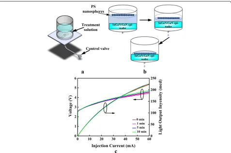
The equipment required to obtain a periodic PS NS array on InGaN/GaN LED through the dip-drop method is very simple and easy to prepare. It comprises a glass container with a hole at the bottom (main container) and a tuning control valve connected to the hole, as shown in Fig. 1 (a). Different volumes of deionized (DI)
Fabrication of InGaN/GaN blue LEDs with a Periodic PS NS Array on an ITO Layer
The epi-wafers of InGaN/GaN blue LEDs were grown on a c-face (0001) sapphire substrate by using a metal-organic chemical vapor deposition system. The device structure consists of a GaN buffer layer grown at a low temperature, a highly Si-doped n-type GaN layer, an InGaN/GaN multiple quantum wells (MQWs) active region, and an Mg-doped p-type GaN layer. The ITO was deposited on the p-type GaN layer as a transparent con-ductive layer to spread the injection current. The wafer was then patterned using the standard photolithographic process to define square mesas as the emitting regions by partially etching the exposed ITO/p-GaN/InGaN/GaN MQWs/n-GaN. A Ti/Pt/Au alloy was used as the ohmic contact metal on the p- and n-GaN contact regions, and the wafer was then alloyed in an N2atmosphere for 5 min
at 450 °C. The size of the emission window for the InGaN/GaN LEDs with ITO was 300 × 300μm2. The fin-ished wafer was placed in the PS NSs suspension to deposit the compact PS NS array on ITO layer.
Results and Discussion
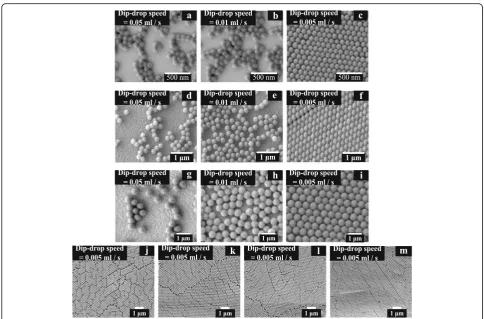
Fig.2a–ishow scanning electron microscopy (SEM) im-ages of the PS NSs with diameters of 100, 200, and
500 nm, on the ITO coated glass substrate, with average dip-drop speeds of 0.05, 0.01, and 0.005 mL/s. The con-centrations of the PS NS suspensions were 4.1 × 10¹¹ spheres/cm−3 for the 100-nm PS NSs, 5.1 × 10¹⁰ spheres/cm−3 for the 200-nm PS NS, and 3.2 × 10⁹ spheres/cm−3for the 500-nm PS NS. The PS NSs exhib-ited a widely dispersed distribution on ITO-coated glass substrate under a high average dip-drop speed, but they formed a compact array as the average dip-drop speed was decreased, as shown in Fig. 2. The arrangement of the PS NSs depends on the shape of the liquid surface, which is related to the lateral capillary force [30]. The lateral capillary force can be classified as a floating force or an immersion force. Floating force is caused by the particle weight and Archimedes force, whereas immersion force results from capillary action [31]. Dur-ing the dip-drop process, the floatDur-ing force dominated because of the effect of gravity. The floating force can be attractive or repulsive between two PS NSs depending on the shape of the surface between the air and aqueous solution. High average dip-drop speed causes a dramatic perturbation in PS NS suspension near the tuning con-trol valve, and the perturbation results in a convex sur-face between the air and aqueous solution, leading to a repulsive floating force between two PS NSs. The PS
a
b
c
[image:3.595.60.538.86.402.2]NSs were separated by the repulsive floating force dur-ing the dip-drop process, resultdur-ing in a disordered PS NS arrangement on the ITO-coated glass substrate, as observed in Fig. 2a, d, g. When the average dip-drop speed was decreased to 0.01 mL/s, the perturbation near the tuning control valve was alleviated, as shown in Fig.2b,e,h. This weak perturbation caused a low repul-sive floating force and yielded a smaller space between two PS NSs than that at the dip-drop speed of 0.05 mL/ s. As the average dip-drop speed was decreased to 0.005 mL/s, the shape of the surface between the air and the aqueous solution became concave, generating an at-tractive floating force between the two PS NSs during the dip-drop process. The attractive floating force can result in a compact PS NS array on the ITO-coated glass substrate, as shown in Fig. 2c, f, i. In addition, PS NSs with diameters of 200 and 500 nm exhibited a more compact arrangement on the ITO-coated glass substrate compared with 100-nm-diameter PS NSs under a similar average dip-drop speed because a concave shape surface between the air and aqueous solution was easily formed
for PS NSs with large diameters. When the average dip-drop speed was further reduced to < 0.005 mL/s, the PS NS array fabricated using the dip-drop method be-came impractical for LEDs because of the low through-put. To find the distribution of the compact PS NSs array on the 0.5 × 0.5-mm2 ITO-coated glass substrate, Fig. 2j–m shows the SEM images of 200-nm-diameter PS NSs under the average dip-drop speeds of 0.005 mL/ s at the regions of upper-right, upper-left, lower-right, and lower-left of ITO-coated glass substrate. These im-ages represent a uniform distributing and compact PS NSs array over the ITO-coated glass substrate, suggest-ing that InGaN/GaN LED with a uniform and compact PS NSs array window layer can be proposed by using dip-drop method.
The concentration of the PS NS suspension also af-fects the PS NS arrangement and layer number of the PS NS array. PS NS suspensions with high concentra-tions result in compact PS NS arrays with monolayer or multilayers, whereas suspensions with low concentration might generate loose or compact PS NS arrays with
a b c
d e f
g h i
j k l m
Fig. 2SEM images of PS NSs with diameter of 100, 200, and 500 nm at the average dip-drop speed ofa,d,g0.05 mL/s;b,e,h0.01 mL/s; andc, f,i0.005 mL/s, and the SEM images of PS NSs with 200 nm and average dip-drop speeds of 0.005 mL/s at the regions ofjupper-right,k upper-left,llower-right, andmlower-left of 0.5 × 0.5 mm2ITO-coated glass substrate . The concentrations of DI water-diluted PS NS suspension were
4.1 × 10¹¹spheres/cm−3for the 100-nm PS NSs, 5.1 × 10¹⁰spheres/cm−3for the 200-nm PS NSs, and 3.2 × 10⁹spheres/cm−3for the 500-nm
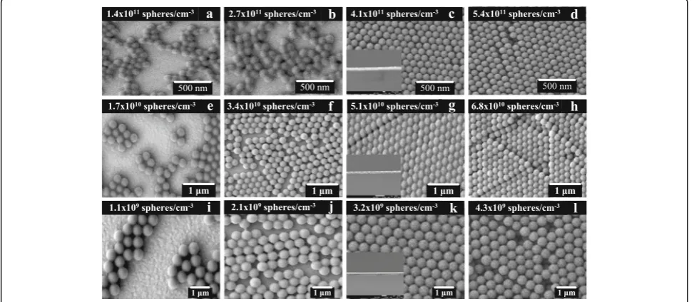
[image:4.595.55.540.85.404.2]monolayers. Multilayer PS NS arrays have shortcomings such as low transmittance, difficult definition for the PS NS period, and low reliability, making them unsuitable for LED applications. The optimal concentration of the PS NS suspension must be determined to obtain com-pact monolayer PS NS array. In this study, the concen-tration of a PS NS suspension was defined as the ratio of the number of PS NSs and the volume of the suspen-sion. Figure3 shows the SEM images of PS NSs on the ITO-coated glass substrate for various PS NS suspension concentrations: (a) 1.4 × 10¹¹, (b) 2.7 × 10¹¹, (c) 4.1 × 10¹¹, and (d) 5.4 × 10¹¹sphere/cm−3for 100-nm PS NSs; (e) 1.7 × 10¹⁰, (f ) 3.4 × 10¹⁰, (g) 5.1 × 10¹⁰, and (h) 6.8 × 10¹⁰ sphere/cm−3for 200-nm PS NSs; and (i) 1.1 × 10⁹, (j) 2.1 × 10⁹, (k) 3.2 × 10⁹, and (l) 4.3 × 10⁹sphere/cm−3 for 500-nm PS NSs with an average dip-drop speed of 0.005 mL/s. When the concentration of the PS NS sus-pension was < 4.1 × 10¹¹sphere/cm−3for 100-nm PS NSs, < 5.1 × 10¹⁰sphere/cm−3for 200-nm PS NSs, and < 3.2 × 10⁹ sphere/cm−3for 500-nm PS NSs, some areas of the ITO-coated glass substrate were free of PS NSs, as shown in Fig. 3a, b, e, f, i, j. When the concentration was in-creased to 4.1 × 10¹¹ sphere/cm−3 for 100-nm PS NSs, 5.1 × 10¹⁰sphere/cm−3for 200-nm PS NSs, and 3.2 × 10⁹ sphere/cm−3for 500-nm PS NSs, a compact PS NS array of monolayers covered the ITO-coated glass substrate, as shown in Fig.3c,g,k. The insets of Fig.3c,g,kshow the cross-section SEM images of PS NSs on the ITO-coated glass substrate under the PS NS suspension concentra-tions of 4.1 × 10¹¹sphere/cm−3for 100-nm PS NSs, 5.1 ×
1010 sphere/cm−3 for 200-nm PS NSs, and 3.2 × 10⁹ sphere/cm−3for 500-nm PS NSs. A compact PS NS mono-layer can be formed on the ITO-coated glass substrate under above concentrations of PS NS suspensions and dip-drop speed. The PS NSs in the high-concentration PS
NS suspension were denser than those in the
low-concentration PS NS suspension. During the dip-drop process, the attractive floating force formed a compact PS NS array of monolayers and a dispersed PS NS array on the ITO-coated glass substrate under the high- and low-concentration PS NS suspensions, respectively, because insufficient PS NSs were available to cover the ITO-coated glass substrate under the low-concentration PS NS suspen-sion. When the concentration of the PS NS suspension was further increased to 5.4 × 10¹¹sphere/cm−3for 100-nm PS NSs, 6.8 × 10¹⁰sphere/cm−3for 200-nm PS NSs, and 4.3 × 10⁹sphere/cm−3for 500-nm PS NSs, the ITO-coated glass substrate was covered by a compact PS NS array of multi-layers because excessively, many PS NSs participated in the deposition. The excess PS NSs reached the surface of the compact PS NS array of the monolayer and then stuck to it to form the compact PS NS array of multilayers.
The light escape cone of an InGaN/GaN LED is limited because of the high refractive index contrast between GaN and air, resulting in a low LEE. Letkbe the wave vector of the escape cone; then,
k¼kNþkL ð1Þ
wherekN and kL are the wave vectors normal to device
a b c d
e f g h
i j k l
Fig. 3SEM images of PS NSs with PS NS suspension concentrations ofa1.4 × 1011,b2.7 × 1011,c4.1 × 1011, andd5.4 × 1011sphere/cm−3for
100-nm PS NSs;e1.7 × 1010,f3.4 × 1010,g5.1 × 1010, andh6.8 × 1010sphere/cm−3for 200-nm PS NSs; andi1.1 × 109,j2.1 × 109,k3.2 × 109, and
l4.3 × 109sphere/cm−3for 500-nm PS NSs at an average dip-drop speed of 0.005 mL/s. The insets ofc,g,andkrepresent the cross-section SEM
images of PS NSs with PS NS suspension concentrations of 4.1 × 10¹¹sphere/cm−3for 100-nm PS NSs, 5.1 × 10¹⁰sphere/cm−3for 200-nm PS NSs,
[image:5.595.56.543.463.675.2]and in-plane, respectively. With the periodic PS NS array window layer on InGaN/GaN LED, if the refractive index periodicity of a periodic PS NS array diffracts the wave-guided modes above a certain cutoff frequency into exter-nally propagating modes, the in-plane wave vector changes tokWG+ nkPS, wherekWGis the wave vector of the wave-guided light parallel to the device, andkPSis the reciprocal wave vector of the periodic PS NS array, given by
kPS¼ð2π=xλÞ^axþð2π=yλÞ^ay ð2Þ
where xλand yλare periods in thex andy directions of PS NS array. For a periodic PS NS array, the original in-plane wave vector,kL, changes tok`L and k`and can be expressed as
k0
L¼kLþnkPS ð3Þ
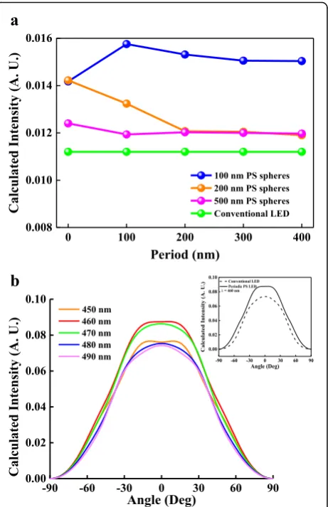
where n is an integer. The light escape cone can be im-proved by changing the periods in thexandydirections to modulate kPS; thus, the LEE of InGaN/GaN LED can be enhanced by reducingk´L. However, the optimal periods in the x and y directions relative to the cutoff frequency to satisfy the emission wavelength of InGaN/GaN blue LED are difficult to obtain through experimental processes. To simplify the investigation, Rsoft software (Cybernet Ltd.), fullwave Sim Add-on Module with three-dimensional FDTD method, and Rsoft LED Utility were used to calcu-late the extracted light intensity from p-GaN to free space for InGaN/GaN blue LEDs without and with the PS NS array window layers with various periods in thexandy di-rections. Figure4apresents the calculated light intensity as a function of the period for LEDs with PS NS array win-dow layers with 100-, 200-, and 500-nm-diameter PS NSs and conventional InGaN/GaN LEDs. The calculated light intensities for the LEDs with the PS NS window layers (blue, yellow, and red curves) were higher than that for the conventional LEDs as shown in Fig. 4a. In addition, the LED with periodic PS NS arrays of the diameter and the periods inxandydirections of 100, 100, and 100 nm has the highest calculated light intensity and shows an en-hanced factor of 1.4 as compared to the LED without PS NS array. This was because the light escape cone for InGaN/GaN LEDs with periodic monolayer PS NS arrays can be improved by adjustingkPS, thereby enhancing the LEE of InGaN/GaN LEDs with periodic PS NS array win-dow layers. To obtain the maximum light intensity for InGaN/GaN LEDs, the optimal diameter and the periods inxandydirections for the PS NS array were calculated as 100, 100, and 100 nm. Furthermore, to comprehend the enhanced LEE of InGaN/GaN LEDs with optimal periodic PS NS array related to the diffraction mode, the extracted light intensity from p-GaN to free space for InGaN/GaN blue LED without and with the optimal PS NS array win-dow layers under different emission wavelength and angle
was calculated. Figure4bshows the calculated light inten-sity as a function of varied angle under the different emis-sion wavelength, and the inset of Fig. 4b displays the angular spectra of InGaN/GaN blue LED with the optimal periodic PS NS array window layer and without PS NS array window layer under emission wavelength of 460 nm. The InGaN/GaN LED with optimal periodic PS NS array emitted at wavelength of 460 nm performs the highest and widest spectrum as compared to those with optimal periodic PS NS array emitted at 450, 470, 480, and 490 nm and InGaN/GaN LED without PS NS array be-cause it satisfies the guide mode diffracted into air by the optimal periodic PS NS array.
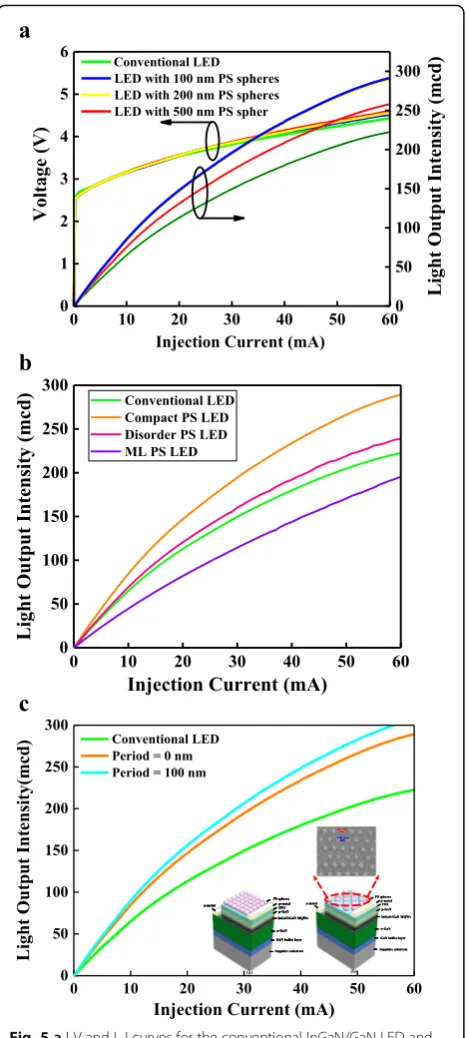
Figure5ashows the I-V and L-I curves of the InGaN/ GaN LEDs without and with the window layer formed by a compact monolayer PS NS array of 100-, 200-, and 500-nm-diameter PS NSs. Under the injection current of
a
b
[image:6.595.308.539.87.444.2]20 mA, the forward voltages for InGaN/GaN LEDs with-out and with the compact PS NS array were 3.54, 3.55, 3.55, and 3.55 V. The similar forward voltages for InGaN/GaN LEDs with and without PS NS array win-dow layers were attributed to them having the same epi-taxial structure. Additionally, the forward resistance for InGaN/GaN LEDs without PS NS array window layers was slightly lower than those with PS NS array window layers, because the ITO transparent conduction layer was degraded by the oxygen plasma during the hydro-philic process. The light output intensities for InGaN/ GaN LEDs without and with the 100-, 200-, and 500-nm PS NS array window layers were 112.9, 146.8, 148.0, and 131.1 mcd, respectively, as shown in Fig. 5a. The light output intensities of InGaN/GaN LEDs without and with the PS NS array window layer showed trends similar to the calculated results in Fig. 4. The photons emitted from the InGaN/GaN active region underwent TIR at the ITO/air interface because they were outside the light escape cone. However, the InGaN/GaN LEDs with PS NS array window layers changed the in-plane vector (kL`), resulting in an enhanced LEE; therefore, the light
output intensity of InGaN/GaN LEDs with PS NS array window layers can be increased. In addition, the incident angle of the emission light at the interface between the PS NS array and air was affected by the PS NSs because of the nonplanar interface as well as the textural struc-ture. Consequently, the periodic PS NS array window layer enhanced the LEE of the InGaN/GaN LEDs. Figure 5b shows the L-I curves of the conventional InGaN/GaN LED and those InGaN/GaN LEDs with compact, disorder, and multilayer PS array window layers. The light output intensity of InGaN/GaN LED with disorder PS layer shows a slightly higher than con-ventional InGaN/GaN LED because the photons can be partially out-coupled at the interface of air/ITO by the disorder PS window layer. In addition, the light output intensity of InGaN/GaN LED with multilayer PS array window layer is lower than conventional InGaN/GaN LED because of the low transmittance (< 80%) for the multilayer PS array. Figure5cpresents the L-I curves of the conventional InGaN/GaN LEDs and those with com-pact and periodic PS NS array window layers. The diam-eter and the periods inxandydirections for periodic PS NS arrays were 100, 100, and 100 nm, respectively, satis-fying the optimality condition calculated from Fig. 4. The periodic PS NS array can be obtained by etching the compact PS NS array of 200-nm PS NSs, and the inset of Fig.5cshows the schematic structures of InGaN/GaN LEDs with compact and periodic PS array and SEM image of etched 100-nm PS NS array with periods of 100 and 100 nm in the x and y directions. The InGaN/ GaN LED with the window layer of periodic 100-nm PS NS array with periods in the x and y directions of 100
a
b
c
[image:7.595.58.292.86.606.2]and 100 nm exhibited the highest light output intensity, as shown in Fig.5c, which was in agreement with the calcu-lated results in Fig.4. The InGaN/GaN LEDs with the op-timal periodic PS NS array window layers yielded a 38% increase in light output intensity compared with those without PS NS arrays because of the improved LEE. In addition, insets of Fig.5cand Fig.2findicate that the PS NSs show a well adherent on ITO and a less etching dam-age during the post-deposition etching process.
Table1lists the average forward voltages and light out-put intensities at the injection current of 20 mA for the se-lected chips from different position of InGaN/GaN wafers with optimal PS NS array window layers made of three different runs under the same condition. A uniform and reliable arrangement of PS NSs on the InGaN/GaN wafers was extremely noteworthy because this is the main factor affecting the performance of InGaN/GaN LEDs. The period and size of the PS NSs on the InGaN/GaN wafers were relatively similar; the device-to-device standard devi-ation of measured enhancement of emission intensity was about 1.4%, and the variations were approximately 1.9% for the forward voltage and 2.9% for the light output in-tensity under the same driving current.
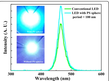
Figure 6 shows the electroluminescence spectra as a function of wavelength for the conventional InGaN/GaN LEDs and the InGaN/GaN LEDs with the optimal periodic PS NS array window layers under the driving current of 20 mA. The light output intensity at 465.5 nm and full width at half maximum of the emission spectrum for the InGaN/GaN LEDs with the optimal periodic PS NS array window layers were stronger and narrower than those of the conventional InGaN/GaN LEDs. The guided light that is emitted from the InGaN/GaN active region underwent TIR and could not phase match to the radiation modes
when the amplitude of the in-plane wave vector in the semiconductor was higher than that in the air [9,32]. The periodic PS NS array window layers could modulate the amplitude of the in-plane wave vector in the semicon-ductor to less than that in air, and therefore, the light was emitted from the semiconductor with the periodic PS NS array because the phase of the guided modes matched the radiation modes, resulting in a high light output intensity and a narrow emission spectrum. The insets of Fig.6show the micrographs of light emission for the conventional InGaN/GaN LEDs and the InGaN/GaN LEDs with the optimal periodic PS NS array window layers. The light output intensity for the InGaN/GaN LEDs with the opti-mal periodic PS NS array window layers was higher than that of the conventional InGaN/GaN LEDs because of the improved LEE.
Conclusion
[image:8.595.307.539.86.259.2]PS NS array window layers can improve the LEE of InGaN/GaN LEDs. A compact monolayer PS NS array was obtained by adjusting the average dip-drop speed and PS suspension concentration. The optimal average dip-drop speed and PS NS suspension concentration to obtain a compact monolayer PS NS array were 0.005 mL/s and 4.1 × 10¹¹ sphere/cm−3, respectively, for 100-nm PS NSs; 0.005 mL/s and 5.1 × 10¹⁰sphere/cm−3, respectively, for 200-nm PS NSs; and 0.005 mL/s and 3.2 × 10⁹ sphere/cm−3, respectively, for 500-nm PS NSs. The calculated and experimental results indicated that the periodic PS NS array window layer with PS NS diameter of 100 nm and periods of 100 nm in thexand y directions effectively enhanced the LEE of the InGaN/ GaN LEDs. The InGaN/GaN LEDs with the optimal periodic PS NS array window layer yielded a 38% in-crease in light output intensity compared with that of
Table 1The average turn-on voltage and light output intensity for selected chips from different position of InGaN/GaN LED wafers with the optimal PS NS arrangement (PS NS diameter of 100 nm and period of 100 nm) on an ITO window layer under a 20-mA driving current
Chip no. Turn-on voltage (V) at 20 mA
Light output intensity (mcd) at 20 mA
1 3.65 155.9
2 3.65 154.3
3 3.66 153.1
4 3.65 151.8
5 3.72 156.4
6 3.71 154.2
7 3.67 152.4
8 3.68 154.7
9 3.67 153.3
10 3.68 156.1
[image:8.595.56.291.569.731.2]the conventional InGaN/GaN LED under a 20-mA driv-ing current because of the high LEE.
Abbreviations
EQE:External quantum efficiency; FDTD: Finite-difference time-domain; ITO: Indium-tin-oxide; I-V: current-voltage; LED: Light-emitting diode; LEE: Light extraction efficiency; L-I: Light output intensity-current; PCs: Photonic crystals; PS NS: Polystyrene nanosphere; SEM: Scanning electron microscopy; TIR: Total internal reflection
Funding
The authors gratefully acknowledge the financial support of the Ministry of Science and Technology, ROC (103-2221-E-150-033-MY2).
Availability of Data and Materials
The datasets supporting the conclusions of this manuscript are included within the manuscript.
Authors’Contributions
PHL carried out the experimental design and data analysis. CDY simulated the compact and periodic PC NS array by using FDTD. YSY carried out the experimental process and measurement. JHL carried out the LED simulation. All authors read and approved the final manuscript.
Competing Interests
The authors declare that they have no competing interests.
Publisher’s Note
Springer Nature remains neutral with regard to jurisdictional claims in published maps and institutional affiliations.
Author details
1Institute of Electro-Optical and Materials Science, National Formosa
University, 64 Wen-Hwa Rd, Hu-Wei 623, Yun-Lin, Taiwan.2Department of Microelectronic Engineering, National Kaohsiung Marine University, Kaohsiung 811, Taiwan.
Received: 6 February 2018 Accepted: 6 June 2018
References
1. Zhmakin AI (2011) Enhancement of light extraction from light emitting diodes. Phys Rpt 498:189–241
2. Chen HC, Lin CC, Wang HW, Tsai MA, Tseng PC, Tsai YL, Han HW, Li ZY, Chang YA, Kuo HC, Yu P, Lin SH (2011) Efficiency enhancement in single-junction InGaP solar cells by using self-assembled nanospheres. Photon Technol Letts 23:691–693
3. Chen BL, Zhou QG, Mcintosh DC, Yuan JR, Chen YJ, Sun WL, Campbell JC, Holmes AI (2012) Natural lithography nano-sphere texturing as antireflective layer on InP-based pin photodiodes. electron Letts 48:1340–1341 4. Joannopoulos JD, Meade RD, Win JN (1995) Photonic crystals. Princeton
University Press, New Jersey
5. Adawi AM, Kullock R, Turner JL, Vasilev C, Lidzey DG, Tahraoui A, Fry PW, Gibson D, Smith E, Foden C, Roberts M, Qureshi F, Athanassopoulou N (2006) Improving the light extraction efficiency of polymeric light emitting diodes using two-dimensional photonic crystals. Organic Electron 7:222–228 6. Wierer JJ, Krames MR, Epler JE, Gardner NF, Craford MG, Wendt JR, Simmons
JA, Sigalas MM (2004) InGaN/GaN quantum-well heterostructure light-emitting diodes employing photonic crystal structure. Appl. Phys. Letts. 84:3885–3887 7. McFroddy K, David A, Matioli E, Iza M, Nakamura S, DenBaars S, Speck JS,
Weisbuch C, Hu EL (2008) Directional emission control and increased light extraction in GaN photonic crystal light emitting diodes. Appl. Phys. Letts. 93:103502
8. Wang SC, Cheng YW, Yin YF, Su LY, Hung YJ, Huang JJ (2011) Interactions of diffraction modes contributed from surface photonic crystals and nanoholes in a GaN-based light-emitting diodes. J Lightwave Technol 29: 3372–3376
9. Chou Y, Li HW, Yin YF, Wang YT, Lin YC, Lin DW, Wu YR, Kuo HC, Huang JJ (2014) Polarization ratio enhancement of a-plane GaN light emitting diodes by asymmetric two-dimensional photonic crystal. J Appl Phys 115:193107
10. Shin YC, Kim DH, Chae DJ, Yang JW, Shim JI, Park JM, Ho KM, Constant K, Ryu HY, Kim TG (2010) Effects of nanometer-scale photonic crystal structures on the light extraction from GaN light-emitting diodes. IEEE J Quantum Electron 46:1375–1380
11. Wu GM, Yen CC, Tsai BH, Chien HW (2011) Preparation and characterization of GaN photonic crystal arrays by focused ion beam technology. Surf Coat Technol 206:801–805
12. Kim SH, Lee KD, Kim JY, Kwon MK, Park SJ (2007) Fabrication of photonic crystal structures on light emitting diodes by nanoimprint lithography. Nanotechnol 18:055306
13. Zhang Q, Li KH, Choi HW (2012) Polarized emission from InGaN light-emitting diodes with self-assembled nanosphere coatings. IEEE Photon Technol Lett 24:1642–1645
14. Ee YK, Arif RA, Tansu N, Kumnorkaew P, Gilchrist JF (2007) Enhancement of light extraction efficiency of InGaN quantum wells light emitting diodes using SiO2/polystyrene microlens arrays. Appl Phys Letts 91:221107
15. Schubert EF (2003) Light-emitting diodes. Cambridge University Press, Cambridge
16. Nakamura S, Fasol G (1997) The blue laser diode. Springer, New York 17. Koike M, Shibata N, Kato H, Takahashi Y (2002) Development of high
efficiency GaN-based multiquantum-well light-emitting diodes and their application. IEEE J Sel Topics Quantum Electron 8:271–277
18. Schubert EF, Kim JK (2005) Solid-state light sources getting smart. Science 308:1247–1278
19. Narukawa Y, Niki I, Izuno K, Yamada M, Murazaki Y, Mukai T (2002) Phosphor-conversion white light emitting diode using InGaN near-ultraviolet chip. J Appl Phys 41:L371–L373
20. Torma PT, Svensk O, Ali M, Suihkonen S, Sopanen M, Odnoblyudov MA, Bougrov VE (2009) Maskless roughening of sapphire substrates for enhanced light extraction of nitride based blue LEDs. Solid State Electron 53:166–169
21. Lee JH, Oh JT, Choi SB, Kim YC, Cho HI, Lee JH (2008) Enhancement of InGaN-based vertical LED with concavely patterned surface using patterned sapphire substrate. IEEE Photon Technol Lett 20:345–347
22. Kissinger S, Jeong SM, Yun SH, Lee SJ, Kim DW, Lee IH, Lee CR (2010) Enhancement in emission angle of the blue LED chip fabrication on lens patterned sapphire (0001). Solid State Electron 54:509–515
23. Wang CC, Ku H, Liu CC, Chong KK, Hung CI, Wang YH, Houng MP (2007) Enhancement of the light output performance for GaN-based light-emitting diodes by bottom pillar structure. Appl Phys Lett 91:121109–1–121109–3 24. Huang HW, Kao CC, Chu JT, Liang WD, Kuo HC, Wang SC, Yu CC (2006)
Improvement of InGaN/GaN light emitting diode performance with a nano-roughened p-GaN surface by excimer laser-irradiation. Mater Chem Phys 99: 414–417
25. Huh C, Lee KS, Kang EJ, Park SJ (2003) Improved light-output and electrical performance of InGaN-based light-emitting diode by microroughening of the p-GaN surface. J Appl Phys 93:9283–9385
26. Hou CH, Tseng SZ, Chan CH, Chen TJ, Chien HT, Hsiao FL, Chiu HK, Lee CC, Tsai YL, Chen CC (2009) Output power enhancement of light-emitting diodes via two-dimensional hole arrays generated by a monolayer of microspheres. Appl Phys Lett 95:133105–1–133105–3
27. Lin CF, Yang ZJ, Zheng JH, Dai JJ (2005) Enhanced light output in nitride-based light-emitting diodes by roughening the mesa sidewall. IEEE Photon Technol Lett 7:2038–2040
28. Lee SJ, Lee J, Kim S, Jeon H (2007) Fabrication of reflective GaN mesa sidewalls for the application to high extraction efficiency LEDs. Phys Stat Solidi (c) 7:2625–2628
29. Ee YK, Kumnorkaew P, Arif RA, Tong H, Zhao HP, Gilchrist JF, Tansu N (2009) Optimization of light extraction efficiency of III-nitride LEDs with self-assembled colloidal-based microlenses. IEEE J Sel Top Quantum Electron 15:1218–1225 30. Denkov ND, Velev OD, Kralchevsky PA, Ivanov IB, Yoshimura H, Nagayama K
(1992) Mechanism of formation of two-dimensional crystals from latex particles on substrates. Langmuir 8:3183–3190
31. Kralchevsky PA, Nagayama K (1994) Capillary forces between colloidal particles. Langmuir 10:23–36