http://dx.doi.org/10.4236/eng.2014.61001
The Implementation of the Surface Charging Effects in
Three-Dimensional Simulations of SiO
2
Etching
Profile Evolution
Branislav Radjenović, Marija Radmilović-Radjenović
Institute of Physics, University of Belgrade, Zemun, Serbia Email: [email protected]
Received August 2,2013; revised September 2, 2013; accepted September 9, 2013
Copyright © 2014 Branislav Radjenović, Marija Radmilović-Radjenović. This is an open access article distributed under the Creative Commons Attribution License, which permits unrestricted use, distribution, and reproduction in any medium, provided the original work is properly cited. In accordance of the Creative Commons Attribution License all Copyrights © 2014 are reserved for SCIRP and the owner of the intellectual property Branislav Radjenović, Marija Radmilović-Radjenović. All Copyright © 2014 are guarded by law and by SCIRP as a guardian.
ABSTRACT
Refined control of etched profile in microelectronic devices during plasma etching process is one of the most im-portant tasks of front-end and back-end microelectronic devices manufacturing technologies. A comprehensive simulation of etching profile evolution requires knowledge of the etching rates at all the points of the profile sur-face during the etching process. Electrons do not contribute directly to the material removal, but they are the source, together with positive ions, of the profile charging that has many negative consequences on the final out-come of the process especially in the case of insulating material etching. The ability to simulate feature charging was added to the 3D level set profile evolution simulator described earlier. The ion and electron fluxes were computed along the feature using Monte Carlo method. The surface potential profiles and electric field for the entire feature were generated by solving Laplace equation using finite elements method. Calculations were per-formed in the case of simplified model of Ar+/CF4 non-equilibrium plasma etching of SiO2.
KEYWORDS
Plasma Etching; Level Set Method; Profile Charging; Finite Elements Method
1. Introduction
The profile surface evolution itself in plasma etching, deposition and lithography development is a significant challenge for numerical methods for interface tracking itself. Level set methods for evolving interfaces [1,2] are specially designed for profiles which can develop sharp corners, change topology and undergo orders of magni- tude changes in speed. Additionally, etching submicron features in insulating materials such as SiO2 or materials masked with insulators, e.g., photoresist-masked polysi- licon, are accompanied by feature charging effects caused by the differences in electron and ion angular distributions [3,4]. In general, the motion of ions incident at the wafer surface on the electrode is more directional than that of electrons. The difference causes the electron shading effect at the etched feature, thus generating posi- tive potential at the deep trench bottom. This charging
effect induces many serious plasma process induced damage problems such as bowing, trenching, reactive ion etching lag, and notching [5]. The reduction in the device size and multilayer structures requires a high-aspect ratio in the SiO2 etching. As the aspect ratio increases, the charging effect becomes more profound. The negative charge that might develop on the sidewalls can bend the trajectories of the ions passing close to them. This bend- ing effect may contribute to micro trenching. In addition, etching rate reduction with time and notching of polysi- licon sidewalls during the over etching step have been attributed in part to feature charging effects.
movement via level set method, particle fluxes calcula- tions using Monte-Carlo method and the electric field (generated by the profile charge) calculations on the ba-sis of the finite elements method.
2. Simulation Procedure
2.1. Level Set Method
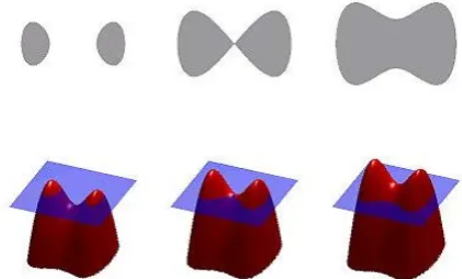
[image:2.595.66.277.579.706.2]The basic idea behind the level set method is to represent the surface in question at a certain time t as the zero level set (with respect to the space variables) of a certain func-tion ϕ (t, x), the so called level set function shown in
Figure 1. The initial surface is given by {x|ϕ(0,x) = 0}. The evolution of the surface in time is caused by the sur-face processes in the case of the etching. The velocity of the point on the surface normal to the surface will be denoted by R(t, x), and is called velocity function. The velocity function generally depends on the time and space variables and we assume that it is defined on the whole simulation domain. At a later time t > 0, the sur-face is as well the zero level set of the function ϕ(t, x). Namely, it can be defined as a set of points {x|ϕ(t, x) = 0}. This leads to the level set equation in Hamilton-Ja- cobi form [6]:
( )
(
,)
0H t x t
ϕ ϕ
∂ + ∇ =
∂ (1)
in the unknown function ϕ (t, x), where Hamiltonian function is given by H = R (t, x)|∇φ(t, x)| and where ϕ(0, x) = 0 determines the initial surface. Several approaches for solving level set equations exist which increase accu- racy while decreasing computational effort. The most important are narrow band level set method, widely used in etching process modeling tools, and recently devel- oped sparse-filed method [3]. The sparse-field method use an approximation to the level set function that makes it feasible to recompute the neighborhood of the zero level set at each time step. As a result, the number of computations increases with the size of the surface, ra- ther than with the resolution of the grid.
Figure 1. Examples of various level set function depending on the initial surface.
We say that Hamiltonian function H is convex if the following condition is fulfilled:
2 0, i j x x H φ φ ∂ ≥
∂ ∂ (2)
where φxi is a partial derivative of φ(t,x)with respect of
xi. The non-convex Hamiltonians are characteristic for
plasma etching and deposition simulations. During these processes the etching (deposition) rate, that defines the surface velocity function R(t,x), depends on the geome- tric characteristics of the profile surface itself, or more precisely, on the angle of the incidence of the incoming particles. In the cases under study here we shall consider an etching beam coming down in the vertical direction. These conditions are characteristic for ion milling tech- nology, but angular dependence of the etching rates ap- pears, more or less, in all etching processes. The simplest finite difference scheme that can be applied in these cas- es is the Lax-Friedrichs scheme, one that relies on the central difference approximation to the numerical flux function, and preserves monotonicity through a second- order linear smoothing term. It is shown [6] that it is possible to use the Lax-Friedrichs scheme in conjunction with the sparse field method, and to preserve sharp inter- faces and corners by optimizing the amount of smoothing in it. This is of special importance in the simulations of the etching processes in which spatially localized effects appear, like notching and microtrenching.
2.2. Particle Fluxes Calculations
the boundaries above the profile surface, periodic condi- tions are assumed.
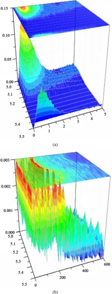
[image:3.595.77.270.194.698.2]The energy and angular distribution functions for Ar+ ions and electrons, used as the boundary conditions for the calculations of electron and ion fluxes incident on the profile surface, are obtained by particle-in-cell (PIC) calculations using XPDC1 code [11-13] and shown in
Figure 2.
(a)
(b)
Figure 2. a) Electron Energy Distribution Function (EEDF) and b) Ion Energy Distribution Function (IEDF) calculated by using PIC/MCC code [11,12].
2.3. Electric Fields Calculations
Finite difference method cannot be used when the geo- metry of the problem is irregular, as it is usual for the etching profiles. So, it naturally to use finite elements method. The calculations of the electric fields in this pa- per are performed by integrating a general finite element solver GetDP [14,15] in our simulation framework. GetDP is a thorough implementation of discrete differen- tial forms calculus, and uses mixed finite elements to discretize de Rham-type complexes in one, two and three dimensions. Meshing of the computational domain is carried out by TetGen tetrahedral mesh generator [16]. TetGen generates the boundary constrained high quality (Delaunay) meshes, suitable for numerical simulation using finite element and finite volume methods. As a part of the post-processing procedure the electric fields, ob- tained on the unstructured meshes, are recalculated on the Cartesian rectangular domains containing the regions of the particles movement. In this manner, the electric field on the particles could be calculated by simple trili- near interpolation. Details about the integration of the whole simulation cycle and the etching rate calculations using particle fluxes could be found elsewhere.
3. Results and Discussions
Here we will present some calculations illustrating our approach in etching profile evolution simulation. Al- though a complete self-consistent cycle that includes profile charging and its influence on the charged particles motion is already implemented, we do not have repre- sentative results yet. The reason is the lack of appropriate computational resources, since the Monte Carlo step re- quires enormous number of particles in every level set step, in order to get satisfying statistics. So, here we present some results of the profile charging calculations for the fixed profile surface.
All the calculations are performed on 128 × 128 × 384 rectangular grid. The initial profile surface is a rectangle deep with dimensions 0.1 × 0.15 × 0.1 µm. Above the profile surface is the trench region. From its top the par- ticles involved in etching process come from, while bel- low is the non-etched material. In the case of the ion en- hanced chemical etching the dependence of the surface velocity on the incident angle is simple: V = V0 cosθ. In
Figure 3. Etching profile evolution during equidistant time steps (0 s, 30 s, 60 s, 90 s and 120 s).
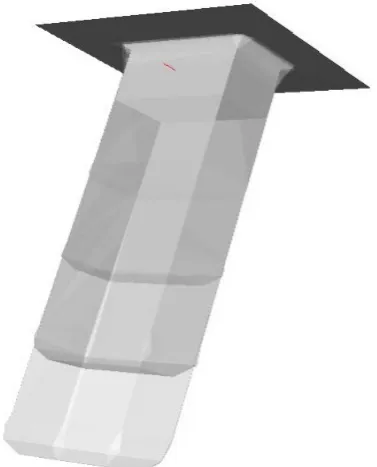
Figure 4. The surface mesh generated by Tetgen [16].
[image:4.595.313.534.312.506.2]the tetrahedral mesh corresponding to the last profile in
Figure 3 is shown. This mesh defines the profile surface for the subsequent particle flux and electric field calcula- tions.
Collisions in the simulation domain are neglected be- cause mean-free path of ions and electrons is much long- er than the simulation domain size. Also, the probability that more than two particles exist in the simulation space at the same time is very low because the life time of ions or electrons in the simulation region is much shorter than the incident time interval. The particle fluxes on profile are given in Figure 5. The neutral and the electron fluxes distributions are similar: they are concentrated on the top of the wafer and upper portion of the sidewalls, while the ions, due its directionality, are accumulated at the bottom of the profile. Solving the Laplace equation with such a charge distribution as boundary condition leads to the potential cut depicted inFigure 6.
[image:4.595.80.266.367.719.2]Figure 5. Space charge density on the profile surface [Q/m2].
[image:4.595.311.538.537.711.2]The maximal value of the potential at the bottom of the profile is somewhat bigger than the average ion energy, while the top surface is slightly negatively bi- ased.
The electric field vectors on the profile surface are shown inFigure 7. It is obvious the field stimulate notch creation by directing the ions toward sidewalls. At the very the top the field accelerate the ions downward, but it quickly changes direction at the lower positions of the profile. The zero field border height is determined by the etching plasma parameters.
4. Conclusion
[image:5.595.71.282.372.712.2]Plasma processing is indeed one of the crucial modern technologies that have made a significant impact on fa- brication of integrated circuits (IC) and consequently in electronics and consumer goods in general. Damage to ICs during manufacturing as a result of charging of the dielectrics during finalization of interconnects is both reducing the profitability and reducing the ability to reach large sizes of microchips and make complex sys- tem integration on a single chip. So, realistic three di- mensional etching profile simulations are urgently needed,
Figure 7. Electric field on the profile surface [V/m].
but still lacking. It is understandable that realistic calcu- lations should include complex surface reactions set, the effects of the profile charging, polymer deposition, as well as better statistic (greater number of particles) in the Monte Carlo step of the calculations, which is usually limited by the available computational resources.
Acknowledgements
The present work has been supported by the Ministry of Education and Science, Republic of Serbai, Projects O171037 and III41011.
REFERENCES
[1] J. Sethian, “Level Set Methods and Fast arching Methods: Evolving Interfaces in Computational Geometry, Fluid Mechanics, Computer Vision and Materials Sciences,” Cambridge University Press, Cambridge, 1998.
[2] S. Osher and R. Fedkiw, “Level Set Method and Dynamic Implicit Surfaces,” Springer, 2002.
[3] K. Hashimoto, “Charge Damage Caused by Electron Shading Effect,” Japanese Journal of Applied Physics, Vol. 33, 1994, pp. 6013-6018.
http://dx.doi.org/10.1143/JJAP.33.6013
[4] H. Ohtake and S. Samukawa, “Charging-Damage-Free and Precise Dielectric Etching in Pulsed C2F4/CF3I Plas- ma,” Journal of Vacuum Science & Technology, Vol. B20, 2002, pp. 1026-1031.
[5] M. Radmilovic-Radjenović, B. Radjenović and M. Savić, “The Surface Charging Effects in Three-Dimensional Simulation of the Profiles of Plasma-Etched Nanostruc- tures,” International Journal of Numerical Modelling, Vol. 24, No. 6, 2011, pp. 535-544.
http://dx.doi.org/10.1002/jnm.798
[6] B. Radjenović, J. K. Lee and M. Radmilovic-Radjenovic, “Sparse Field Level Set Method for Non-Convex Hamil-tonians in 3D Plasma Etching Profile Simulations,” Com- puter Physics Communications, Vol. 174, No. 2, 2006, pp. 127-132.http://dx.doi.org/10.1016/j.cpc.2005.09.010
[7] G. Hwang and K. Giapis, “On the Origin of the Notching Effect during Etching in Uniform High Density Plasmas,”
Journal of Vacuum Science and Technology, Vol. B15, 1997, pp. 70-87.http://dx.doi.org/10.1116/1.589258
[8] A. Mahorowala and H. Sawin, “Etching of Polysilicon in Inductively Coupled Cl2 and HBr Discharges. IV. Calcu-lation of Feature Charging in Profile Evolution,” Journal of Vacuum Science and Technology, Vol. B20, 2002, pp. 1084-1095.http://dx.doi.org/10.1116/1.1481869
[9] B. M. Radjenović, M. D. Radmilović-Radjenović and Z. L. Petrović, “Dynamics of the Profile Charging During SiO2 Etching in Plasma for High Aspect Ratio Trenches,”
IEEE Transactions on Plasma Science, Vol. 36, No. 4, 2008, pp. 874-875.
http://dx.doi.org/10.1109/TPS.2008.920886
Software Engineering and Applications, Vol. 6, 2013, pp. 390-395.http://dx.doi.org/10.4236/jsea.2013.68048
[11] C. K. Birdsall, “Particle-In-Cell Charged-Particle Simula-tions, Plus Monte Carlo Collisions with Neutral Atoms, PIC-MCC,” IEEE Transactions on Plasma Science, Vol. 19, No. 2, 1991, pp. 65-85.
http://dx.doi.org/10.1109/27.106800
[12] J. P. Verboncoeur, “Particle Simulation of Plasmas: Re-view and Advances,” Plasma Physics and Controlled Fu-sion, Vol. 47, 2005, pp. A231-A260.
http://dx.doi.org/10.1088/0741-3335/47/5A/017
[13] H. C. Kim, F. Iza, S. S. Yang, M. Radmlović-Radjenović
and J. K. Lee, “Particle and Fluid Simulations of Low-Temperature Plasma Discharges: Benchmarks and Kinetic Effects,” Journal of Physics D: Applied Physics, Vol. 38, 2005, pp. R283-R301.
http://dx.doi.org/10.1088/0022-3727/38/19/R01
[14] C. Geuzaine, “High Order Hybrid Finite Element Schemes for Maxwell’s Equations Taking Thin Structures and Glo- bal Quantities into Account,” Ph.D. Thesis, Universite de Liege, 2001.
[15] GetDP, http://www.geuz.org/getdp
![Figure 7. Electric field on the profile surface [V/m].](https://thumb-us.123doks.com/thumbv2/123dok_us/7976181.755500/5.595.71.282.372.712/figure-electric-field-profile-surface-v-m.webp)
