Technology (IJRASET)
©IJRASET 2015: All Rights are Reserved
311
Multi-State Switching Cell for Single Phase
Five-Level Inverter
A.Vedavathi1, J. Nagarjuna Reddy2, A. Suresh Kumar3 1
PG student, 2,3Assistant Professor, Department of EEE RGMCET, Kurnool, AP, India
Abstract—for low voltage applications, a new T-type inverter topology based on multi-state switching cell is proposed, when medium (or) high switching frequencies are preferred. In this paper the MSSC application presents two topologies of five level inverter. The T-type inverter topology is compared by the Neutral-Point Clamped topology. As the name indicates T-type the conduction takes place in the form of T-shape. In T-type inverter topology the common emitter configurations are used for the switches, it acts like a bidirectional switch; these switches are used to block the half of the dc-link voltage. Due to the reduced blocking voltage, the switch shows very low switching losses. Thus, the THD of output voltage should be reduced. Since the filter ripple frequency is twice the switching frequency, therefore reducing the magnetic weight and size.
Key words: - Multi-state switching cell, Switch configurations, T-type inverter, Dc-Link Voltage, Auto-transformer.
I. INTRODUCTION
Now a day’s the power electronic converters plays a major role in dc-ac converters, which transforms energy from a dc source into an ac source and these are referred as inverters. The dc input power source is present in the systems like, battery bank, photovoltaic solar panels, fuel cells and the output of a rectifier. Among many applications, inverters are used for inductive heating and uninterrupted power supply systems (UPS) which are being more and more popular in the industry. Practically, dc-ac converter obtains a rectangular output with high harmonic component, which is undesirable for many applications. To minimize this problem, pulse width modulation (PWM) technique is implemented. The term multilevel starts with the three-levels of output voltage in inverter, by increasing the number of levels in the inverter, the output voltages have more steps generating a staircase waveform, which has a reduced harmonic distortion. Multilevel inverters include an array of controlled semiconductor devices with antiparallel diodes and capacitor voltage sources. In multilevel inverters the Neutral-Point Clamped (NPC) converter based on Multi-State Switching Cell is presented in this paper. The T-type inverter consists of two types of cells. One is full bridge switches and another one is half bridge switches. Half bridge switches are connected to that of the dc-link mid-point. These switches have to block the half of the dc-link voltage. Therefore, it is possible to use the IGBTs having a lower voltage rating. Therefore, the conduction losses of the T-type inverter are considerably reduced compared to that of the NPC inverter.
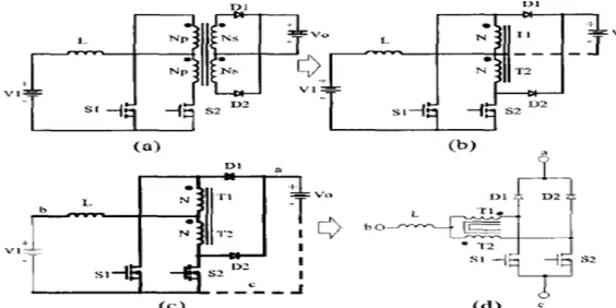
A. The Basic Cell Generating Procedure
The cell generating procedure is as shown in figure (1.1). If we consider a two winding transformer, first the secondary side of the transformer is referred to as the primary side, second the output voltage source Vo is connected to the common point of the switches. Finally from the converter the new switching cell is obtained between the points a, b and c.
[image:2.612.181.463.560.701.2]Technology (IJRASET)
©IJRASET 2015: All Rights are Reserved
312
In order to clarify the issues such as input ripple current, output rms current and also reduce the current stresses on semiconductor devices are performed depends on the number of switching states. A five level inverter based multi-state switching cell is applied to the T-type converter (5L T-Type-MSSC) has some advantages compared with the 5L NPC-MSSC topology : it presents less number of semiconductors, because it does not need clamping diodes, due to this reducing cost of the converter. During the operating intervals, the number of conducting semiconductors is smaller; this will represents the reduction in total losses. And also we can reduce the current stresses on semiconductor devices.
II. FIVE-LEVEL NPC-MSSC TOPOLOGY
The five-level Neutral-Point Clamped topology based on multi-state switching cell is shown in fig (2), consists of eight controlled switches (S1-S8) with respective to the anti-parallel diodes (D1-D8); four clamping diodes (DC1-DC4) are used to clamp the output voltage. One autotransformer with windings N1 and N2 of unitary transformation ratio (1:1) is used to flow the current evenly through the semiconductor switches. One passive filter is used to reduce the high frequency component in the output voltage composed by the inductor (Lo) and capacitor (Co).
Fig (2) five-level NPC-MSSC topology
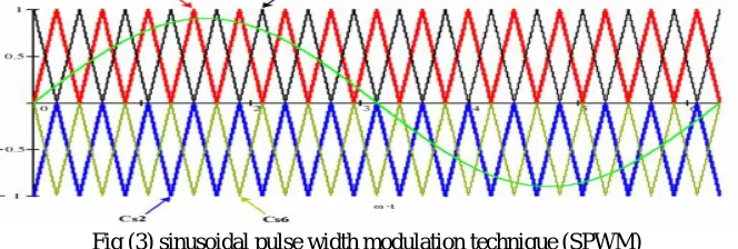
A. Modulation Technique
The engaged modulation technique is the sinusoidal pulse width modulation technique (SPWM), as shown in figure (3).
Fig (3) sinusoidal pulse width modulation technique (SPWM)
The carriers Cs1 and Cs2 can be arranged in vertical shifts, with the signals in phase with each other called phase disposition (PD-PWM). The carriers Cs5 and Cs6 are phase-shifted by the 180 degrees. The drive signals of switches S1, S2, S5 and S6 are obtained from the comparison of the sinusoidal reference voltage with the respective triangular carriers Cs1, Cs2, Cs5 and Cs6. Thus, the drive signals of switches S1 and S5 are phase-shifted by 180 degrees and so the drive signals of switches S2 and S6. The drive signals of switches S3, S4, S7 and S8 are complementary to those for switches S1, S2, S5 and S6 respectively. Applying this modulation technique in the five-level topologies, until the end of entire positive semi-cycle of the sinusoidal reference voltage the switches S2 and S6 are in conduction state. While the switches S1 and S5 are performs the non-conduction state for negative semi-cycle of the sinusoidal reference voltage.
B. Operation Modes
[image:3.612.162.449.254.387.2] [image:3.612.141.473.452.564.2]Technology (IJRASET)
©IJRASET 2015: All Rights are Reserved
313
Non-overlapping mode
The overlapping mode occurs when the switches S1 and S5 or S2 and S6 are having the continuous conduction during the positive and negative semi-cycle of the output voltage. The Non-overlapping mode occurs when the switches S1 and S5 or S2 and S6 are not having the continuous conduction during the positive and negative semi-cycle of the output voltage as shown in figure (4).
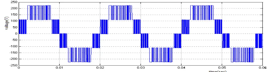
Fig (4) the inverter output voltage during one-cycle
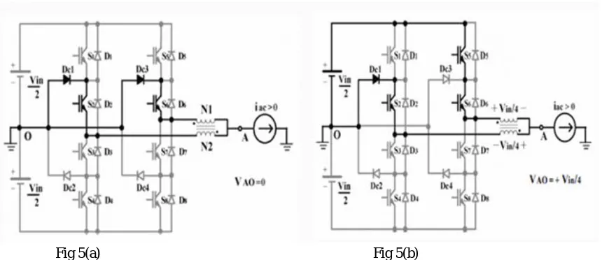
1) Non-Overlapping Mode In The Positive Semi-Cycle: a) Mode 1: The entire positive semi-cycle of the output voltage the switches S2 and S6 are in conducting and the switches S1 and S5 are non-conduction state of operation. During this stage, half of the load current flows through diode Dc1 switch S2, and winding N2. While the remaining half flows through the diode Dc3, switch S6, and winding N1. During this stage, is as shown in figure 5(a), the output voltage VAO is equal to zero.
b) Mode 2:
When the switch S1 is off and S5 is on, half of the load current flows through the input voltage source (Vin), switches S5 and S6, winding N1. While the remaining half flows through diode Dc1, switch S2, and winding N2. During this operation stage, is represented in figure 5(b), the output voltage Vao is equal to +Vin/4. A similar operation stage occurs when switch S1 is on and S5 is off.
Thus the output current is equally shared between the autotransformer windings and the current stresses for the controlled switches and diodes are reduced.
[image:4.612.193.433.139.241.2]Fig 5(a) Fig 5(b) Fig 5 Operation stages in non-overlapping mode
2) Overlapping Mode In Positive Semi-Cycle: a) Mode 1: In this operation mode, switches S2 and S6 are always on, and also the switches S1 and S5 are on, half of the load current flows through switches S1 and S2, and winding N2. The remaining current flows through switches S5 and S6, which is shown in figure 6(a), the output voltage Vao is equal to +Vin/2.
b) Mode 2:
[image:4.612.93.523.427.613.2]Technology (IJRASET)
©IJRASET 2015: All Rights are Reserved
314
output voltage Vao is equal to +Vin/4. A similar operation stage occurs when switch S1 is on and S5 is off. The behaviour of the converter in overlapping modes considering the negative semi-cycle of the output voltage is analogous to that for positive one.
[image:5.612.130.487.108.227.2]Fig 6(a) Fig 6(b) Fig 6 operation modes in overlapping mode
C. Output Voltage
From the previous analysis, it is possible to conclude that the output voltage Vao assumes three possible values for each semi-cycle according to the state of switches, while null voltage exists in both semi-cycles. Therefore the output voltage waveform assumes five levels.
III.PROPOSED TOPOLOGY
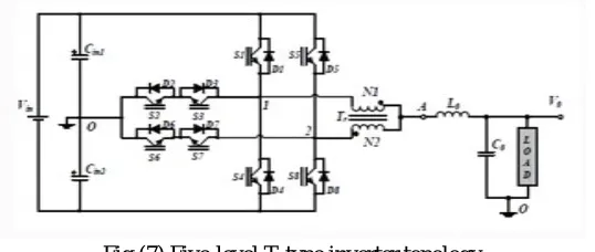
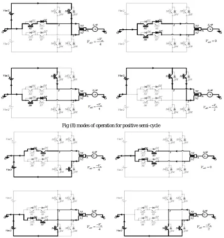
The five-level T-type inverter topology based on MSSC is self-possessed by the following components are as shown in figure (7), eight controlled switches (S1-S8) with respective to the anti-parallel diodes (D1-D8); one autotransformer with windings N1 and N2 and one passive filter is used to reduce the high frequency component in the output voltage composed by inductor and capacitor. In this proposed inverter, an active bidirectional switch to the dc-link mid-point providing superior output voltage quality. Thus a third voltage level is added to the two output levels of each leg of the inverter. Consequently, the output voltage without filter presents five levels.
Fig (7) Five-level T-type inverter topology
The employed modulation technique is same as that of five-level NPC-MSSC topology. And also the modes of operation are same as that of NPC-MSSC topology with two operation modes according to the states of switches:
Overlapping mode Non-overlapping mode
Positive semi-cycle (non-overlapping mode):
The time at the end of the positive semi-cycle of the sinusoidal reference voltage the switches S2 and S6 are on. Mode 1:
The switch S5 starts conducting and S1 is switched off. Fig 8(a) shows this operating stage, where the half of the load current flows through the input voltage source, the switch S5 and winding N2. While the remaining half flows through the intrinsic diode D3, switch S2 and winding N1. During this stage, the output voltage VAO is equal to +Vin/4.
Mode 2:
[image:5.612.174.443.418.532.2]Technology (IJRASET)
©IJRASET 2015: All Rights are Reserved
315
Mode 3:
The switch S1 starts conducting and S5 is switched off. Fig 8(c) shows this operating stage, where the half of the load current flows through the input voltage source, the switch S1 and winding N1. On the other hand, the remaining half of the load current flows through the diode D7, switch S6 and winding N2. During this stage the output voltage is equal to +Vin/4.
Mode 4:
This stage is identical to the second stage of the non-overlapping mode.
Fig (8) modes of operation for positive semi-cycle
Fig (9) modes of operation for negative semi-cycle
Positive semi-cycle (overlapping mode): Mode 1:
[image:6.612.78.538.155.643.2]Technology (IJRASET)
©IJRASET 2015: All Rights are Reserved
316
In this mode, the switch S1 and S5 are turned on. Thus, half of the load current flows through switch S1 and winding N1; while the remaining half flows through switch S5 and winding N2. During this stage, is represented in fig. 8(d), the autotransformer windings are short-circuited and the output voltage VAO is equal to +Vin/2.
Mode 3:
This stage is identical to the third stage of the non-overlapping mode. Mode 4:
This stage is identical to the second stage of the overlapping mode.
[image:7.612.67.487.230.359.2]The five-level T-type inverter topology operating in the overlapping and non-overlapping modes considering the negative semi-cycle of the output voltage is analogous to that of previously explained for positive semi-semi-cycle. Figure (9) shows the operating stages for overlapping and non-overlapping modes in the negative semi-cycle of the sinusoidal reference voltage.
TABLE 1: Switching states for 5LT-type MSSC
Modes of operation S1 S5 S4 S8 VAO
Non-overlapping Mode
Off On off off +Vin/4
Off Off off off 0
on Off off off +Vin/4
on On off off +Vin/2
Overlapping Mode
Off Off off on -Vin/4
Off Off off off 0
Off Off On off -Vin/4
Off Off On on -Vin/2
Output voltage:
The output voltage of proposed inverter VAO presents three possible values for each semi-cycle, according to the conduction states of switches, and the level zero is obtained in both semi-cycles. This way the output voltage waveform presents five-levels.
IV.COMPARISON OF TOPOLOGIES
By comparing the above two topologies, the NPC-MSSC topology, clamping diodes are used for clamp the voltage, but in T-type MSSC topology clamping diodes are necessary, due to this less semiconductors are used in T-type topology by this cost will be reduced. Same rating of IGBTs are preferred for NPC-MSSC topology, different ratings of IGBTs are used for reducing the switching losses in T-type MSSC topology. Common emitter configurations are used to form a bidirectional switch, which has to block the half of the dc-link voltage. No need of switching configurations in NPC-MSSC topology.
V. SIMULATION RESULTS
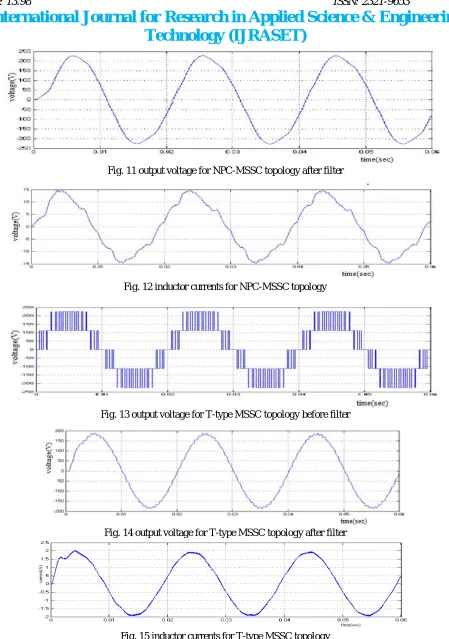
Fig (10) (11), shows the inverter output voltage VO and the five levels of output voltage VAO for NPC-MSSC topology. The THD value of the unfiltered output voltage VAO obtained in the simulation was 43.21%. Fig (13) (14), shows the inverter output voltage VO and the five levels of output voltage VAO for T-type MSSC topology. The THD value of the unfiltered output voltage VAO obtained in the simulation was 38.17%. The current waveforms in the inductor LO are as shown in fig. 11. It can be observed that the load current is divided equally between the autotransformer windings N1 and N2.
[image:7.612.84.529.586.704.2]Technology (IJRASET)
[image:8.612.81.530.32.671.2]©IJRASET 2015: All Rights are Reserved
317
Fig. 11 output voltage for NPC-MSSC topology after filter
Fig. 12 inductor currents for NPC-MSSC topology
Fig. 13 output voltage for T-type MSSC topology before filter
Fig. 14 output voltage for T-type MSSC topology after filter
[image:8.612.84.530.39.338.2]Technology (IJRASET)
[image:9.612.125.514.55.684.2]©IJRASET 2015: All Rights are Reserved
318
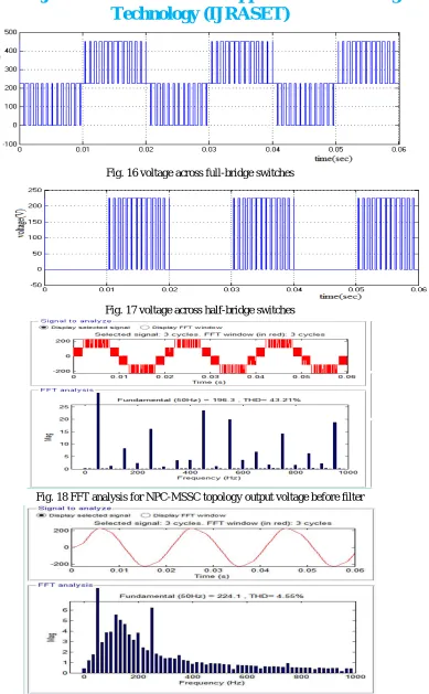
Fig. 16 voltage across full-bridge switches
Fig. 17 voltage across half-bridge switches
Fig. 18 FFT analysis for NPC-MSSC topology output voltage before filter
Technology (IJRASET)
[image:10.612.121.493.53.671.2]©IJRASET 2015: All Rights are Reserved
319
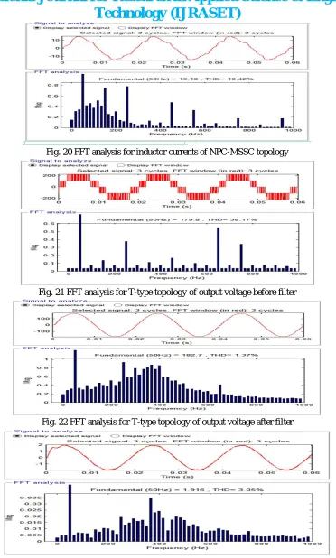
Fig. 20 FFT analysis for inductor currents of NPC-MSSC topology
Fig. 21 FFT analysis for T-type topology of output voltage before filter
Fig. 22 FFT analysis for T-type topology of output voltage after filter
Technology (IJRASET)
©IJRASET 2015: All Rights are Reserved
320
TABLE 2: Comparison table for simulation results
parameters THD of output voltage
without filter%
THD of output voltage with filter%
THD of inductor currents%
Five-level
NPC-MSSC topology 43.21 4.55 10.42
Five-level
T-type MSSC topology
38.17 1.37 3.05
VI.CONCLUSION
An application of multi-state switching cell is applied to the five-level NPC-MSSC and the T-type MSSC was also present in this paper. The proposed topology presents the five levels of output voltage before the filter, and also provides lower harmonic distortion; Weight and size of the magnetic components and cost of the inverter is reduces, because low semiconductor devices are used. Additionally, the 5L T-type-MSSC presents low conduction losses due to current sharing between the semiconductor devices.
VII. ACKNOWLEDGMENT
I would like to express thanks to my advisor J.NAGARJUNA REDDY, Asst.Prof in EEE dept. RGMCET, Nandyal, Andhra Pradesh, India for continuous encouragement throughout the work.
REFERENCES
[1] D. V. Ashok Kumar, et.al, “Advanced Pulse Width Modulation Techniques for Z Source Multi Level Inverter”. World Academy of Science, Engineering and Technology, International Science Index 99, International Journal of Electrical,Computer, Energetic, Electronic and Communication Engineering, 9(3), 337 – 342.
[2] J. Rodriguez, L. G. Franquelo, S. Kouro, J. I. Léon, R. C. Portillo, M.A. M. Prats and M. A. Pérez, “Multilevel converters: an enabling technology for high-power applications, “Proceedings of the IEEE, vol. 97, no. 11, pp. 1786–1817, Nov. 2009.
[3] A. Nabae, I. Takahashi, and H. Akagi, “A new neutral-point-clamped PWM inverter,” IEEE Trans. Ind. Appl., vol. IA-17, no. 5, pp. 518–523, Sep. 1981. [4] T. Bruckner, S. Bernet, and H. Güldner, “The active NPC converter and its loss-balancing control,” IEEE Transactions on Industrial Electronics, vol. 52, no. 3,
pp. 855–868, June 2005.
[5] F. Kieferndorf, M. Basler, L. A. Serpa, J. H. Fabian, A. Coccia and G. A. Scheuer, “ANPC-5L technology applied to medium voltage variable speed drives applications,” in Power Electronics Electrical Drives Automation and Motion (SPEEDAM), International Symposium on, pp. 1718-1725, 2010.
[6] G. V. T. Bascopé and I. Barbi, “Generation of a family of non-isolated DC-DC PWM converters using new three-state switching cells”, in Proc. IEEE PESC’2000, vol. 2, pp. 858–863, June 2000.
[7] R. A. Camara, P. P. Praça, R. P. T. Bascopé and C. M. T. Cruz, “Comparative analisys of performance for single-phase ac-dc converters using FPGA for UPS applications,” in 28th Annual IEEE Applied Power Electronics Conference and Exposition (APEC), vol. 1. pp. 1852-1858, 2013.
[8] R. Hausmann and I. Barbi, “Three-phase dc-ac converter using four-state switching cell,” IEEE Transactions on Power Electronics, vol. 26, pp. 1857-1867, 2011.
[9] R. P. T. Bascopé, J. A. F. Neto and G. V. T. Bascopé, “Multi-state commutation cells to increase current capacity of multi-level inverters,” in Telecommunications Energy Conference (INTELEC), Amsterdam, Netherlands, 2011.
[10] J. A. F. Neto, R. P. T. Bascopé, C. M. Cruz, R. G. A. Cacau and G. V. T. Bascopé, “Comparative evaluation of three single-phase NPC inverters,” in Industry Applications (INDUSCON), 10th IEEE/IAS International Conference on, pp. 1-8, Fortaleza, Brazil, 2012.
[11] M. Schweitzer and J.W. Kolar, “High efficiency drive system with 3- level T-type inverter,” in Proc. 14th Eur. Conf. Power Electron. Appl., pp. 1–10, 2011. [12] M. Schweitzer and J. W. Kolar, “Design and implementation of a highly efficient three-level T-type converter for low-voltage applications,” in Power