Full Length Research Article
OPTIMAL STRUCTURES FOR CASCADED MULTILEVEL INVERTER
1
Gayathri, U.,
1Nithiya, M.,
1Shekanas, K. and
2*Ramkumar, S.
1
Department of EEE, Surya of Group of Institutions, Vikiravandi
2
Department of EEE, R.M.D Engineering College, Chennai
ARTICLE INFO ABSTRACT
The general function of a multilevel inverter is to synthesize a desired output voltage from several levels of dc voltages as inputs. In order to increase the steps in the output voltage, a new H- bridge topology is recommended which benefits from a series connection of several sub-multilevel inverters. In addition, for producing an output voltage with a constant number of steps, there are different configurations with a different number of components. In this paper, the optimal structures for H- bridge topology are investigated for various objectives such as minimum number of switches and dc voltage sources and minimum standing voltage on the switches for producing the maximum output voltage steps. Two new algorithms for determining the dc voltage sources magnitudes have been proposed. Finally, in order to verify the theoretical issues, simulation results for 25 level inverter with a maximum output voltage of 120V are presented.
Copyright © 2014 Gayathri et al. This is an open access article distributed under the Creative Commons Attribution License, which permits unrestricted use, distribution, and reproduction in any medium, provided the original work is properly cited.
INTRODUCTION
The concept of utilizing multiple small voltage levels to perform power conversion was carried over thirty years ago (Babaei et al., 2007; Baker et al., 1975; Baker, 1980). The advantages include enriched power quality, less electro-magnetic compatibility, low switching losses and high voltage blocking capability (Khomfoi and Tolbert, 2007). Three bench mark topologies namely cascaded diode clamped and flying capacitor multilevel inverter have been came into existence in the past four decades (Rech and Pinheiro, 2007). Baker et al patented the cascaded H-bridge and diode clamped structures in 1975 and 1980. It utilizes isolated dc sources or a bank of series capacitors to split the dc bus voltage to create higher power quality (Baker, 1980; Nabae et al., 1980). In Mixed-level hybrid multiMixed-level cells (Rodriguez et al., 2007), the H-bridge cells of the cascaded leg are substituted with diode-clamped or flying-capacitors (Meynard and Foch, 1992). To reduce the number of separate dc sources for high-voltage high-power applications, new configurations have also been presented (Manjrekar et al., 2000; Du et al., 2006). Recently, several multilevel converter topologies have been developed (Babaei et al., 2005; Babaei, 2008).
*Corresponding author: Ramkumar, S.
Department of EEE, R.M.D Engineering College, Chennai
The cascaded H-bridge inverter is a very modular solution based on a widely commercialized product (Ogasawara et al., 1992; Tuncer and Tatar, 2007). This has a good effect on the reliability and maintenance of the system since the cells have high availability, intrinsic reliability and a relatively low cost. Unfortunately, the inverters do have some disadvantages (Teichmann et al., 2000). One particular disadvantage is the greater number of power semiconductor switches needed. Although, lower voltage rated switches can be utilized in a cascaded multilevel converter, each switch requires a related gate driver and protection circuits (Lu et al., 2005). This may cause the overall system to be more expensive and complex. The topology consists of series connected sub-multilevel inverter blocks using H- Bridge Inverters (Ueda et al., 1995). In this topology, the modulation strategies and the structures of the different cells and the required switches are the same (Stemmler and Guggenbach, 1993). Thus, in order to reduce the cost of the inverter, it is necessary to introduce an optimal structure with the minimum number of components. In this paper, in order to generate all the steps (odd and even) at the output voltage, two new procedures for calculating the magnitudes of the required dc voltage sources are proposed (Baiju et al., 2003). In addition, this paper proposes an optimal structure for this type of multilevel converter with a high number of steps associated with a low number of power
ISSN:
2230-9926
International Journal of Development Research
Vol. 4, Issue, 3, pp. 613-618, March,2014
DEVELOPMENT RESEARCH
Article History:
Received 08th January, 2014
Received in revised form 11th February, 2014
Accepted 15th February, 2014
Published online 14th March, 2014 Key words:
switches and dc voltage sources (Du et al., 2006). This results in a reduction in cost for the converter (Corzine et al., 2004). Finally, this paper includes a design example of a multilevel inverter.
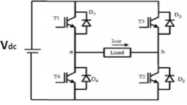
[image:2.595.38.288.239.437.2]Fig .1. single phase full bridge inverter
Fig. 2. Cascaded sub-multilevel inverter
Cascaded H Bridge Inverter
The basic unit for the multilevel inverter showing in Fig .1 consists of a dc voltage source (with a voltage equal to Vdc)
with four unidirectional switches. It is noted that three levels can be achieved for Vo using the basic unit shown in Fig. 1 and
it can be extended as sub-multilevel structure is also illustrated in Fig. 2. The basic units in series can increase the possible values of Vo. If n dc voltage sources are used in the extended
with k basic units in series as shown in Fig. 2, then the number of output voltage steps (Nstep) and switches (Nswitch) are given
by the following equations, respectively:
)
1
2
(
1
k
j j
step
n
N
k
n
N
switch
4
.
Proposed Algorithms for the Determination of Magnitudes of DC Voltage Sources
As mentioned previously, to determine the values of the dc voltage sources, an algorithm is required to utilize a lower number of dc voltage sources and power switches.
First Proposed Algorithm
In this algorithm, it is proposed that the values for all of the dc voltage sources for generating odd and even steps can be calculated using the following relationships:
First stage
1
1 1 , 1
, 2 1 , 1
n
i j dc
dc
v
v
v
v
v
(1)j=1, 2, 3,………..,n1
Second stage:
dc
v
v
v
2,1
2,2
2
dc
j
n
v
v
,2
(
2
1
1
)
(2)j=1, 2, 3,………..,n2
1
1 1 , 2
,
2
n
i i dc
j
v
v
v
1
1 1
1 ,
,
2
m
j n
l j dc
m j
j
v
v
v
mth stage:
dc j
j m
j
v
v
v
v
,
,1
,2
4
Second Proposed Algorithm
For a greater reduction in the variety of the values of the dc voltage sources, another new algorithm is proposed as follows:
First stage:
dc
j
v
v
v
v
,1
2,1
3,1
(3)j=1, 2, 3,………..,n1
Second Stage:
1
1 1 , 2
,
2
n
i i dc
j
v
v
v
(
2
n
1
1
)
v
dc
3
1 1 , 2
,
1
2
i i
dc
v
v
v
]
[
2
v
1,1v
2,1v
3,1v
dc
Similarly
]
[
2
1,1 2,1 3,12 ,
3
v
v
v
v
]
[
2
1,1 2,1 3,12 , 3 2 , 2 2 ,
1
v
v
v
v
v
v
v
dc
(4)j=1, 2, 3,………..,n2
mth Stage:
Let the position of cell be l, the total number of dc sources in cell be ni and the total number of stages be m.
]
[
4
3,1 3,2 3,33 , 3 3 ,
2
v
v
v
v
v
v
dc
1 1 1 1 , ,2
m j n l j dc m j jv
v
v
(5)Optimal Structures Based on the Topology Proposed
For a constant number of dc voltage sources and their possible arrangements in different stages, it is possible to obtain a different number of steps at the output voltage utilizing a different number of power switches (Song and Lai, 2001). For example with four dc voltage sources and 16 power switches, if there are two dc voltage sources in the first stage and one in the second stage, the number of steps at the output will be 15. While using two dc voltage sources in each stage and utilizing the same number of power switches the output steps will be equal to 25 (Rodriguez et al., 2007). By utilizing more dc voltage sources, the repetition of such states will grow (Klumpner and Blaabjerg, 2006). There is a great variety of configurations for a constant number of dc voltage sources. Therefore, to choose the optimal structure for a special state because this ability leads to a reduction in the size, weight and cost of the converter (Faiz and Siahkolah, 2003). Considering the great variety of existing configurations, the optimal structures are proposed in the following sections.
Optimal Structure for the Minimum Number of Switches with a Constant Number of dc Voltage Sources
The question concerning the proposed structure is that if the number of dc voltage sources (Ncapacitor) is constant, which
topology can provide a minimum number of switches (Nswitch).
Suppose the converter consists of a series of k stages each with
ni dc voltage sources (i = 1, 2,………….., k). Thus
cte
n
n
n
n
N
capacitor
1
2
3...
m
(6)Considering (6), the number of switches is given in (7),
)]
1
(
2
[
)]
1
(
2
[
)]
1
(
2
[
1
2
mswitch
n
n
n
N
(7)Optimal structures for a minimum number of switches with a constant number of voltage steps
The objective of a multilevel converter is to obtain the maximum step number with a minimum of switches. The question concerning the proposed structure is that if the number of voltage steps (Nstep) is constant, which topology can
provide a minimum number of switches.
The number of levels and switches can be represented as
No of levels
2
n
1
(8)No of switches
4
n
(9)Suppose a converter consists of a series of m stages each with
ni (i = 1, 2, ……, m) dc voltage sources as shown in Fig. 2.
The number of switches is given by (9). Considering, the number of output steps is given as follows:
)
1
2
(
1
m j j stepn
N
(10)g
x
n
N
m j jstep
)
1
2
(
1 (11)Using the method of the lagrange multipliers, such problems can be solved. For this method, the cost function is defined as follows
g
N
f
switch
(12)In the above equation, λ is the lagrange multiplier and the function g is as follows
x
N
g
step
(13)According to the method of the lagrange multipliers, the minimum number of switches can be calculated by solving the following equations
0
i i switch in
g
n
N
n
f
(14)0
g
f
(15)The above equations can be rewritten as follows
)
(
N
x
N
f
switch
step
(16)x
n
n
f
m j j m ji
)
1
2
(
[
4
1 1
(17)Notice that nj (j = 1, 2, ……, k) is an integer and thus Sj is an
integer too. If nj is substituted by an integer between zero and
infinity, the answer-set for Sj will be
}
....
,...
7
,
5
,
3
,
1
{
js
(18)Considering the above answer-set for Sj is obtained as
follows
s
s
s
s
s
1
2
3
...
...
m
(19)From equation (19), it is obvious that
n
n
n
n
n
1
2
3
...
...
m
(20)The above equation denotes that in order to use the minimum number of switches for producing the maximum number of voltage steps, the number of switches must be the same in all stages. Substituting (18) into (5) and (8) results in
m
n
N
switch
4
.
k
m
(21)m m
j
step
n
n
N
(
2
1
)
(
2
1
)
(22)m
step
n
N
(
2
1
)
(23)The above equations can be written as
)
1
2
ln(
)
ln(
n
N
m
step (24)Therefore the minimum number of switches will be
)
1
2
ln(
)
ln(
4
n
N
n
N
switch step (25)Since Nstep is constant, Nswitch will be minimized when 2(n+1)
= ln(2n+1) tends to the minimum.
Optimal structure for the minimum number of dc voltage sources with a constant number of voltage steps
The next question is that if Nstep is the number of voltage steps
considered for voltage Vo, which topology with a minimum
number of dc voltage sources can satisfy this need. Suppose the converter consists of a series of ’k’ stages each with ni (i =
1, 2, …….,m) dc voltage sources. The number of output voltage steps is given by (10) and the number of dc voltage sources is given as follows
m
capacitor
n
n
n
N
1
2
...
(26)Using the method of the lagrange multiplier the optimal answer is obtained by solving the following equation
m
forj
s
j
3
1
,
2
,...
(27)
m
n
n
n
n
1
2
3
...
...
(28)The second method for proving the above conclusion is as follows. It can be proven that the minimum number of dc voltage sources may be obtained for an equal number of dc voltage sources in each stage. The number of dc voltage sources is given by
)
*
(
n
m
N
capacitor
(29)}
)
1
2
ln(
)
ln(
{
*
n
N
n
N
capacitor step (30)
Since Nstep is constant, Ncapacitor will be minimized when n= ln
[2n + 1] tends to minimum. Where n = 1 gives the minimum number of dc voltage sources to realize Nstep values for the
voltage.
Optimal structures for the minimum standing voltage of switches with constant number of voltage steps
The voltage and current ratings of the switches in a multilevel converter play important role in the cost and realization of the multilevel converter. In all topologies, the currents of all the switches are equal to the rated current of the load. However, this is, not true for the voltage. The question is that if Nstep
voltages are considered for Vo, which topology uses the
switches with the minimum voltage. Suppose that the peak voltage of the switches is represented by:
k
j
j stage
switch
v
v
1
, (31)
I
n the above equation, Vstage; j represents the peak voltage of
the switches in stage j. Therefore, it can be considered as a
criterion for the comparison of different topologies from the maximum voltage on the switches. A lower criterion indicates that a smaller voltage is applied at the terminal of the switches in the topology, which is considered an advantage. With reference to the following equations can be obtained.
The maximum standing voltage
s
1,1(
v
s1,1)
is follow1 , 1
, 3 1 , 2 1 , 1 1 ,
1
...
ns
v
v
v
v
v
dc n
s
v
v
1,1
(
2
1
)
(32)The maximum standing voltage
s
3,1(
v
s3,1)
is as follows1 , 1
, 3 1 , 2 1 ,
3
...
.
ns
v
v
v
v
1 , 1
, 3 1 , 2 1 , 1 1 ), 1 2
( n
...
ns
v
v
v
v
v
(33)Thus the maximum standing voltage on the switches in the first stage is calculated as follows
)
(
2
1,1 3,1 (2 1),1 (2 1),11
,
s
s
s n
s nstage
v
v
v
v
v
dc n
nv
.
2
1
(34)]
...
...
)[
2
(
1,1 2,1 3,1 1,1
k n
switch
n
v
v
v
v
v
(35)
v
switch(
n
2
n1)[
1
x
x
2...
...
x
k1]
v
dc
x
2
n1
1
dc k n
switch
v
x
x
n
v
)
1
1
)(
2
(
1
(36)
]
1
2
1
]
)
1
2
ln(
)
(ln
)[
1
2
[(
2
.
1
n step n
dc n
n
N
v
n
(37)SIMULATION RESULTS
To show the performance of the multilevel inverter, using proposed algorithm, the multilevel inverter shown in Fig.2 is simulated using MATLAB R2010b. Several modulation strategies have been reported for multilevel converters (Hosseini Aghdam et al., 2008; Lu et al., 2005; Du et al., 2006; Tuncer and Tatar, 2007; Lopez et al., 2008). In this paper, the multicarrier PWM (MCPWM) switching technique is employed to verify the feasibility of the proposed optimal structures for the topology depicted in Fig. 2. For simulation analysis, 2 cells per stage and 2 stages are chosen. The input cell voltages have been calculated using the proposed optimal structures are V1, 1= V2, 1=10V and V1, 2= V2, 2=50V and R-L
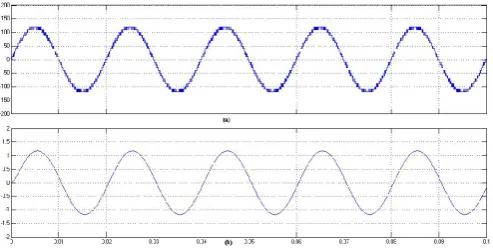
load (R = 100 and L = 55mH). Fig. 3 shows the simulation results for the output voltage and current for 25 level respectively. Therefore, the amplitude of the output voltage is found to be 84.27V. The amplitude of the output current obtained from simulation is 1A. The THDs of the output voltage and current based on the simulation are 4.18% and 2.55%, respectively.
Fig. 3. (a) Output voltage waveform (b) Load current waveform
Conclusion
In this paper, two new algorithms for the determination of the magnitudes of dc voltage sources have been proposed for the cascaded H-bridge topology. It was shown that the structure consisting of units with two dc voltage sources is the best case to keep the minimum number of switches for a certain number of voltage steps.
REFERENCES
Babaei, E., S. H. Hosseini, G. B. Gharehpetian, M. Tarafdar Haque and M. Sabahi, “Reduction of dc voltage sources and switches in asymmetrical multilevel converters using a
novel topology,” Elsevier Journal of Electric Power
System Research, Vol. 77, No. 8, pp. 1073- 1085, Jun.
2007.
Baker, R. H. and L. H. Bannister, “Electric power converter,” U.S. Patent, 3 867 643, Feb. 1975.
Baker, R. H. “High-voltage converter circuit,” U.S. Patent, 04 203 151, May 1980.
Khomfoi, S. and L. M. Tolbert, Multilevel power converters, Power electronics handbook, Elsevier, ISBN 978-0-12-088479-7, 2nd edn., Chapter 17, pp. 451-482, 2007. Nabae, A., I. Takahashi and H. Akagi, “A new neutral-point
clamped PWM inverter,” in Proceeding of IAS, pp. 761-766, 1980.
Meynard, T. A. and H. Foch, “Multi-level conversion: high voltage choppers and voltage source inverters,” in Proceeding of PESC, Vol.1, pp. 397-403, 1992.
Ogasawara, S., J. Takagali, H. Akagi and A. Nabae, “A novel control scheme of a parallel current-controlled PWM inverter,” IEEE Trans. Ind. Appl., Vol. 28, No. 5, pp. 1023-1030, Sep./Oct. 1992.
Ueda, F., M. Asao and K. Tsuboi, “Parallel-connections of pulsewidth modulated inverters using current sharing reactors,” IEEE Trans. Power Electron., Nol. 10, No. 6, pp. 673-679, Nov. 1995.
Baiju, M. R., K. Gopakumar, K. K. Mohapatra, V. T. Somasekharand L. Umannand, “A high resolution multilevel voltage space phasor generation for an open-end winding induction motor drive,” EuropeanPower Electronics and Drive Journal, Vol. 13, No. 4, pp. 29-37,
Sep./Oct./Nov. 2003.
Stemmler, H. and P. Guggenbach, “Configurations of high-power voltage source inverters drives,” in Proceeding of European Conference on Power Electronics and Applications, Vol. 5, pp. 7-14, 1993.
Corzine, K. A., M. W. Wielebski, F. Z. Peng and J. Wang, “Control of cascaded multi-level inverters,” IEEE Trans. Power Electron., Vol. 19 , No. 3, pp. 732-738, May 2004. Rech, C. and J. R. Pinheiro, “Hybrid multilevel converters:
Unified analysis and design considerations,” IEEE Trans. Ind. Electron., Vol. 54, No. 2, pp. 1092-1104, Apr. 2007. Rodriguez, J., J. Lai and F. Z. Peng, “Multilevel inverters: a
survey of topologies, controls, and applications,” IEEE Trans. Ind. Electron., Vol. 49, No. 4, pp. 724-738, Aug. 2002.
Manjrekar, M., P. K. Steimer and T. Lipo, “Hybrid multilevel power conversion system: a competitive solution for high-power applications”, IEEE Trans. Ind. Appl., Vol. 36, No. 3, pp. 834-841, May/Jun. 2000.
Du, Z., L. M. Tolbert, J. N. Chiasson and B. Ozpineci, “A cascaded multilevel inverter using a single dc power source,” in Proceeding of APEC, pp. 426-430, 2006. Teichmann, R., K. O. Brian and S. Bernet, “Comparison of
multilevel ARCP topologies,” in Proceeding of Int. Power Electronics Conf., pp. 2035-2040, 2000.
Song, B. M. and J. S. Lai, “A multilevel soft-switching inverter with inductor coupling,” IEEE Trans. Ind. Appl., Vol. 37, pp. 628-636, Mar./Apr. 2001.
Babaei, E., M. Tarafdar Haque and S. H. Hosseini, “A novel structure for multilevel converters,” in Proceeding of Eighth International Conference on Electrical Machines and Systems, Vol. 2, pp. 1278-1283, 2005.
industrial medium-voltage drives,” IEEE Trans. Ind. Electron., Vol. 54, No. 6, pp. 2930-2945, Dec. 2007. Babaei, E. “A cascade multilevel converter topology with
reduced number of switches,” IEEE Trans. Power Electron., Vol. 23, No. 6, pp. 2657-2664, Nov. 2008. Klumpner, C. and F. Blaabjerg, “Using reverse blocking
IGBTs in power converters for adjustable speed drives,” IEEE Trans. Ind. Appl., Vol. 42, No. 3, pp. 807-816, May/Jun. 2006.
Faiz, J. and B. Siahkolah, “New solid-state onload tap-changers topology for distribution transformers,” IEEE Trans. Power Del., Vol. 18, No. 1,pp. 136-141, Jan. 2003. Hosseini Aghdam, M. G., S. H. Fathi, G. B. Gharehpetian, “A
novel switching algorithm to balance conduction losses in power semiconductor devices of full-bridge inverters,” European Transactions on Electrical Power, Vol. 18, No. 7, pp. 694-708, Oct. 2008.
Lu, S., K. A. Corzine and T. K. Fikse, “Advanced control of cascaded multilevel drives based on P-Q theory,” in Proceeding of EMDC, pp. 1415-1422, 2005.
Du, Z., L. M. Tolbert and J. N. Chiasson, “Active harmonic elimination for multilevel converters,” IEEE Trans. Power. Electron., Vol. 21, No. 2, pp. 459-469, Mar. 2006.
Tuncer, S., and Y. Tatar, “A new approach for selecting the switching states of SVPWM algorithm in multilevel inverter,” European Transactions on Electrical Power, Vol. 17, No. 1, pp. 81-85, Jan./Feb. 2007.
Lopez, O., J. Alvarez, J. Doval-Gandoy and F. D. Freijedo, “Multilevel multiphase space vector PWM algorithm,” IEEE Trans. Ind. Electron., Vol. 55, No. 5, pp. 1933-1942, May 2008.