Abstract: To solve the problem of the mismatched voltage levels between the dynamic lower voltage of the fuel cell stack and the required constant higher voltage (400V) of the DC link bus of the inverter for fuel cell vehicles, a Boost three-level DC-DC converter with a diode rectification quasi-Z source (BTL-DRqZ) is presented in this paper, based on the conventional flying-capacitor Boost three-level DC-DC converter. The operating principle of a wide range voltage-gain for this topology is discussed according to the effective switching states of the converter and the multi-loop energy communication characteristic of the DRqZ source. The relationship between the quasi-Z source net capacitor voltages, the modulation index and the output voltage, is deduced and then the static and dynamic self-balance principle of the flying-capacitor voltage is presented. Furthermore, a Boost three-level DC-DC converter with a synchronous rectification quasi-Z source (BTL-SRqZ) is additionally proposed to improve the conversion efficiency. Finally, a scale-down 1.2 kW BTL-SRqZ prototype has been created, and the maximum efficiency is improved up to 95.66% by using synchronous rectification. The experimental results validate the feasibility of the proposed topology and the correctness of its operating principles. It is suitable for the fuel cell vehicles.
Keywords: Boost three-level DC-DC converter, fuel cell vehicles, Quasi-Z source, synchronous rectification, wide range of voltage-gain.
I. INTRODUCTION
Non-renewable energy sources continue to be consumed and fossil fuel related emissions continue to increase pollution [1~3].
Manuscript received June 28, 2016. Accepted for publication November 1, 2016. This work was supported in part by the National Natural Science Foundation of China under Grants 51577130, and 51207104, and in part by the Research Program of Application Foundation and Advanced Technology of Tianjin China under Grant 15JCQNJC03900.
Yun Zhang, Jilong Shi, Lei Zhou, and Ping Wang are with the School of Electrical Engineering and Automation, Tianjin University, Tianjin 300072,
China (fax: +86-022-27402325; e-mail: [email protected],
[email protected], [email protected], and [email protected]).
Jing Li is with the Department of Electrical and Electronic Engineering, University of Nottingham, Ningbo, China (email: [email protected]).
Mark Sumner is with the Department of Electrical and Electronic
Engineering, University of Nottingham, UK (email:
Changliang Xia is with the School of Electrical Engineering and Automation, Tianjin University, and also with the Tianjin Key Laboratory of Advanced Technology of Electrical Engineering and Energy, Tianjin Polytechnic University, China (e-mail: [email protected]).
With regard to transport, the development of clean-energy vehicles can have a major impact on improving air quality (especially in cities) as well as reducing other fossil fuel related problems [4~6]. The fuel cell vehicle is an important type of the clean-energy vehicle and its obvious advantage is that it provides clean propulsion power with zero emission, as well as higher energy utilization [7~9]. However, the fuel cell usually has a current source characteristic with low output voltage and high output current. In addition, it is difficult to use it to supply an inverter to drive a vehicle, due to its soft output characteristic [10~12]. Therefore, it must be interfaced to the DC link bus of the inverter through a step-up DC-DC converter with a wide range of voltage-gain. The wide gap in voltage levels between the fuel cell stack and the DC link bus can be matched, and stable DC link bus voltage can also be obtained.
Usually the conventional Boost two-level DC-DC converter is employed due to its simple structure [13, 14], but, it suffers from disadvantages including limited voltage-gain, and high voltage stress for its power semiconductors. To alleviate the problem of mismatched voltage levels, the rated voltage of the fuel cell stack has to be increased (increasing the difficulty of assembling the fuel cell stack). At the same time, power semiconductors with higher rated blocking voltage need to be employed and consequently the conduction losses can be improved. In order to reduce the high voltage stress of power semiconductors, Boost three-level DC-DC converters have been proposed, and then the voltage stress can be reduced by half [15~17]. However, there remain two essential problems concerning the interface between the fuel cell stack and the DC-link bus, namely the same limited voltage-gain with that of the Boost two-level converter, and the complicate control required for the flying-capacitor voltage balance of the Boost three-level converter, especially the voltage imbalance of the flying-capacitor in the transient state [18] - this latter may cause power semiconductor failure. It is therefore necessary to solve these problems for fuel cell vehicles, which use the Boost three-level DC-DC converter with a flying capacitor.
As to the non-isolated step-up DC-DC converters with high voltage-gain, the voltage multiplier circuits are adopted to extend the voltage-gain [19]. The switched-inductor structures for step-up DC-DC converters can also obtain high voltage-gain, as well as the switched-capacitor DC-DC converters [20, 21]. However, these step-up DC-DC converters with high voltage-gain are too complex to reduce their cost and size. The quadratic Boost DC-DC converter can also achieve a high
Yun Zhang, Member, IEEE, Jilong Shi, Lei Zhou, Jing Li, Member, IEEE, Mark Sumner, Senior
Member, IEEE, Ping Wang, and Changliang Xia, Senior Member, IEEE
Wide Input-Voltage Range Boost Three-Level
DC-DC Converter with Quasi-Z Source for Fuel
voltage-gain [22]. However, the power semiconductors of the output side (the high voltage side) suffer from high voltage stresses (due to the high output voltage), and create a high dv/dt during switching. Although a large conversion ratio interleaved Boost DC-DC converter using two stages in parallel and one series multiplier stage can convert 24V to 200V [23], there still two diodes in the multiplier stage which suffer from the full output voltage stress. A family of diode-coupled-winding Boost DC-DC converters with a high voltage-gain can perform better than their active-clamp counterparts due to recycled leakage energy [24], achieving a maximum efficiency about 91.7%. Based on [23] and [24], a high voltage-gain interleaved Boost DC-DC converter magnetically coupled to a voltage-double circuit was proposed in [25]. In addition, another high voltage-gain Boost DC-DC converter can obtain higher efficiency, which is based on the three-state commutation cell with additional two transformers (six windings) [26].
Z source net has been applied in the traditional step-up DC-DC converters to achieve the higher voltage-gain [27], but their input and output sides don't share the common ground, which may result in maintenance safety and EMI problems. In addition, the output diode can be replaced by an inductor in the Z source DC-DC converters [28], but the voltage-gain is reduced unexpectedly. The diode rectification quasi-Z (DRqZ) source circuit is another modified energy storage circuit structure which has been proposed for the combination of a low voltage DC source and an inverter [29, 30]. It can also be used in the step-up DC-DC converters with the features of lower capacitor voltages and the common ground [31], but its voltage-gain is the same as the conventional Z source DC-DC converters, and the voltage stress of the power switch is still as high as the output voltage. The coupled inductor based Z source DC-DC converters can achieve high voltage-gain by setting the turn ratio of the coupled inductor [32]. However, the spike voltage of the power switches may be very large due to the leakage inductor of the coupled inductor. In [33], a common grounded Z source DC-DC converter with high voltage-gain is presented by changing the connection way of the grounding, the input source and the load are located on the same side of the Z source, instead of being located on both sides of the Z source. It is analyzed in [33] that the voltage stress of the power semiconductors is reduced in the range of half of the output voltage to nearly the output voltage, when increasing the duty cycle (voltage-gain). In addition, the current stress of the power switch is several times as high as the output current while increasing the duty cycle (voltage-gain).
In this paper, a wide input-voltage range Boost three-level DC-DC converter with a diode rectification quasi-Z source (BTL-DRqZ) is proposed as a solution which can reduce the voltage stress of all semiconductors to half of the output voltage; it also has a common ground for the input and output by using the flying-capacitor three-level structure, and operates well with a high voltage-gain, proper duty cycles (0.5<=d<0.75), and balancing of the voltage of the flying capacitor without additional hardware. Although one more power switch and diode are employed compared to the conventional quasi-Z source Boost DC-DC converter, the lower rated voltage semiconductors with lower on-resistance can replace the higher
rated voltage devices. In addition, the equivalent frequency of the inductor current and the capacitor voltage ripple in the proposed topology is double the switching frequency due to using one additional power switch, diode and flying capacitor, achieved by using the flying-capacitor three-level structure with two phase-shifted 180 degree gate driving signals. These features are beneficial to improve efficiency. In order to improve the efficiency of the proposed converter further, the Boost three-level DC-DC converter with a synchronous rectification quasi-Z source (BTL-SRqZ) is additionally proposed, based on the BTL-DRqZ. This paper is organized as follows: in Section II, the topology of the BTL-DRqZ for fuel cell vehicles is presented. The operation principles of the converter topology with a synchronous rectification quasi-Z source are discussed in Section III. In Section IV, the parameters of all components are designed, and the losses of the proposed topology are analyzed. Then, the experimental results measured from the prototype are analyzed in Section V. Finally, the conclusion is delivered in Section VI.
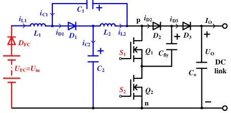
II. TOPOLOGY OF DRQZ SOURCE CONVERTER In order to widen the step-up voltage gain of the Boost DC-DC converter, the DRqZ source net "L1-L2-D1-C1-C2" has
been investigated. The input of the converter is comprised of the voltage source of the fuel cell UFC=Uin and its associated reverse
blocking diode DFC. A three-level DC-DC converter with
flying-capacitor is adopted, to halve the voltage stress on the power devices and also allow Uin and the DC link bus to have a
common ground. The resulting BTL-DRqZ for a fuel cell vehicle is shown in Fig. 1.
UFC=Uin
L1 D1 L2
C1
C2
DFC
D2 D3
Cfly
Co S1
S2
UO DC link iL1
iC1
iD1
iC2
iL2
iD2 iD3
Q1
Q2 p
n
IO
Fig. 1 Proposed Boost three-level DC-DC converter with diode rectification quasi-Z source (BTL-DRqZ) for fuel cell vehicles.
III. OPERATION PRINCIPLES
A. Operation states
According to Fig. 1, there are four switching states "S1S2" in a
switching period, i.e. S1S2={11, 10, 01, 00}, where "1"
represents the power switches Q1, Q2 "ON", and "0" represents
Q1, Q2 "OFF". L1 and L2 are storing energy, while C1 and C2 are
discharging energy when S1S2=11. In the other switching states,
L1 and L2 discharging energy, whereas C1 and C2 are charging.
In addition, the sequence of the switching states in a switching period is related to the duty cycle ranges of the power switches Q1, Q2. For example, Sequence I "01-00-10-00-01" appears
within the range of 0<d1=d2<0.5, while Sequence II
"01-11-10-11-01" can be obtained by the range of 0.5<d1=d2<1,
where d1 and d2 (d1=d2) are the corresponding duty cycles for Q1
and Q2 in a Boost three-level DC-DC converter. However, the
inductors L1 and L2 only discharge in Sequence I, due to the
[image:2.612.326.553.394.505.2]the proposed converter operates within the range of 0.5<d1=d2<1.
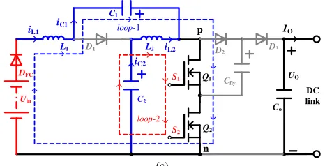
In the active switching states, the energy flow paths between the fuel cell stack source, inductors and capacitors are shown in Fig. 2, and the PWM modulation strategy and important waveforms are illustrated in Fig. 3. In Fig. 2(a), there are three energy flow loops when S1S2=01: in loop-1, L2 is discharging, at the same
time C1 is charging through D1. The inductor current iL2 and the
capacitor voltage UC1 are shown in Fig. 3(e, f); in loop-2, L1 and
Uin in series are discharging, while C2 is charging through DFC
and D1. Thus the inductor current iL1 and the capacitor voltage
UC2 can be illustrated in Fig. 3(d, g); in loop-3, L1, L2 and Uin in
series are discharging, while the flying-capacitor Cfly is charging
through DFC, D1, D2, and Q2. Hence the corresponding voltage
and current waves are shown in Fig. 3(d, e, h, j, k, m). In addition, the instantaneous PWM voltage of the converter Upn
(S1S2=01) is simply the voltage across Cfly, namely Upn=UCfly, as
shown in Fig. 3(n).
When S1S2=10, there are also three energy flow paths as
shown in Fig. 2(b). It can be seen that the difference between S1S2=10 and S1S2=01 is the discharging/charging state of the
flying-capacitor Cfly, e.g. Cfly, Uin, L1, and L2, are in a series
connection and discharge to supply the DC link side through DFC, D1, Q1 and D3. The corresponding voltage and current
waveforms are shown in Fig. 3(d, e, h, i, l, m). At the same time, the instantaneous PWM voltage of the converter Upn(S1S2=10)
is described as Upn=UOUCfly, rather than the voltage across
Cfly, as shown in Fig. 3(n).
In another active switching state S1S2=11, D1 is OFF due to the
reverse voltage of L1. As a result, two energy flow paths are left, as
shown in Fig. 2(c). In loop-1, C1 (which stays in a series
connection with Uin) is discharging, while L1 is charging through
DFC, Q1 and Q2; similarly, C2 is transferring energy to L2 through
Q1 and Q2 in loop-2. Consequently, the instantaneous PWM
voltage of the converter Upn=0 (S1S2=11) can be obtained as
shown in Fig. 3(n).
D3
Co
UO
DC link
Uin
L1 D1 L2
C1
C2 DFC
D2
Cfly
S1
S2 loop-1
loop-2
loop-3
iL1 iC1
iD1
iC2
iL2
iD2
Q1
Q2
n
p IO
(a)
Uin
L1 D1 L2
C1
C2 DFC
D2
Cfly
S1
S2 loop-1
loop-2
loop-3
D3
Co
UO
DC link iL1
iC1
iD1
iC2
iL2
iD3
Q1
Q2
n
p IO
(b)
Uin
L1 D1 L2
C1
C2
DFC Q
1
S2
loop-1
loop-2
D2
Cfly
D3
Co UO
DC link
iL1 iC1
iL2 iC2
Q2 S1
n
p IO
[image:3.612.323.556.51.170.2](c)
Fig. 2 Energy flow paths among the voltage source, inductors and capacitors in effective switching states. (a) S1S2=01 (D1 is ON). (b) S1S2=10 (D1 is ON). (c)
S1S2=11 (D1 is OFF).
B. Operation with wide range of voltage-gain
In order to simplify the explanation, it is assumed the capacitance of the capacitors in Fig. 1 is infinite, as well as the inductance of the inductors. Therefore, capacitors C1, C2 are
seemed to be constant voltage sources, and L1, L2 can be
considered as constant current sources. In addition, the flying-capacitor voltage is half of the output voltage UO, e.g.
UCfly=UO/2. When S1S2=01 or S1S2=10, L1 and L2 are
discharging. Thus iL1 and iL2 are identical in Fig. 2(a, b), and the
voltages across L1 and L2 are also equal (1):
L1_dis= L2_dis
u u (1) By means of Fig. 2(a, b) and KVL (Kirchhoff’s Voltage Laws), the voltage balance equations can be obtained as follows
O
in L1_dis L2_dis
L2_dis C1
in L1_dis C2
2 U
U u u
u U
U u U
(2)
When S1S2=11, L1 and L2 are charging, their voltages uL1_ch and L2_ch
u can be described as follows from Fig. 2(c) and KVL
in C1 L1_ch
C2 L2_ch
U U u
U u
(3)
According to (1) and (2), the discharging voltage across L1 can
be written as (4),
O in
L1_dis 2
2 U
U u
(4)
while the charging voltage of L1 is obtained by virtue of (2)~(4)
O in
L1_ch
2 2 U
U u
(5)
Regarding the charging/discharging time of L1, when S1S2=01
and S1S2=10, the discharging time tL1_dis of L1 is described as
follows by means of the PWM modulation strategy shown in Fig. 3(a~c)
L1_dis 1 2
1 2
[(1 ) (1 )]
t d d T
d d m d
(6)
while the charging time tL1_ch of L1 is written
L1_ch [ 2 (1 1)]
t d d T (7) where d1=d2=d are the duty cycles of Q1 and Q2 respectively, m
0.5
S1
S2
carrier2 carrier1
T T/2
0
m
1
iL1
UC1
(a)
(b)
(c)
(d)
(e)
(f)
iD1
iQ1
(g)
(h)
(i)
iL2
UC2
(j)
iQ2
1
0 11 01 0
1 11 10
(k)
UCfly
1-d1
d2
(l)
(m)
iD2
iD3
Upn
T(n) T/2
0
Uo/2
[image:4.612.330.549.51.179.2]Uo/2
Fig. 3 PWM modulation strategy and important waveforms.
In current continuous mode, the voltage-second balance equation for L1 can be established as follows, by means of the
equal charging and discharging energy in each carrier period
L1_dis L1_dis L1_ch L1_ch
u t u t (8) As a result, the step-up voltage-gain M of the BTL-qZ can be obtained by the combination of (4)~(8)
O
in
2 3 4 U
M
U d
(9)
where 0.5 d 0.75. In addition, the capacitor voltages across C1 and C2 can also be gained by virtue of (2), (4) and (9)
C1 O
C2 O
( 0.5)
(1 )
U d U
U d U
(10)
By means of (9), the proposed topology in Fig. 1 has a wider step-up voltage-gain range, especially the duty cycles of Q1 and
Q2 are kept within the range of
0.5, 0.75
. Consequently, theconventional Boost three-level DC-DC converter’s dilemma between the high voltage-gain and the non-extreme duty cycles can be solved by the proposed topology. In Fig. 4, it is shown the comparison of voltage-gain M via duty cycles d among the conventional Boost three-level converter, the interleaved converter in [23], the common ground converter in [33], and the proposed one. Therefore, the proposed converter in Fig. 1 has a wider range of voltage-gain than those previously presented. Even if it operates with lower voltage-gain (i.e. M=2), the more proper duty cycles
0.5, 0.75
will appear, rather than theextreme low duty cycles in [23] and [33].
0 0.2 0.4 0.6 0.8 1
d 0
10 20 30 40 50
M
Fig. 4 Comparison of voltage-gain M via duty cycles d among conventional Boost three-level converter, interleaved converter in [23], common ground converter in [33], and proposed one.
C. Self-balance of flying-capacitor voltage
According to Fig. 2(a, b), L2 is discharging, and its voltage
uL2_dis is just the voltage across C1
L2_dis C1 1 2 01 10)
u U , (S S , (11) When S1S2=01, D2 and Q2 are ON as shown in Fig. 2(a), so the
flying-capacitor voltage UCfly_01 across Cfly can be described as
follows by (11)
Cfly_01 C2 C1
U U U (12) Similarly, when S1S2=10, Q1 and D3 are ON as shown in Fig.
2(b), the flying-capacitor voltage UCfly_10 can also be obtained
Cfly_10 O ( C2 C1)
U U U U (13) While S1S2=11, Q1 and Q2 are ON, but D2 and D3 are OFF as
shown in Fig. 2(c). Consequently, the flying-capacitor voltage UCfly_11 is maintained. According to (12) and(13), it is
concluded the flying-capacitor voltage UCfly directly depends on
the sum of UC1 and UC2 from the DRqZ source net. Furthermore,
the obvious relationship between UCfly and the output voltage
UO is deduced from (10)
O Cfly
2 U
U (14)
From the analysis above, it can also be further concluded that the flying-capacitor voltage UCfly is clamped by the sum of UC1
and UC2 from the DRqZ source net, and UCfly can follow half the
output voltage UO by this self-balance characteristic, both in the
converter's static and dynamic states. Therefore, extra balanced controls for the flying-capacitor voltage can be removed, and the voltage stress of all power semiconductors can still be constant at half the output voltage.
D. Synchronous rectification operation for quasi-Z source
According to (14) and Fig. 2, the voltage stress of the power semiconductors Q1, Q2, D2 and D3 is half the output voltage.
Regarding the voltage stress of D1 from the DRqZ source
system, its blocking voltage is just the sum of UC1 and UC2 when
S1S2=11, as shown in Fig. 2(c). Therefore, it is also half the
output voltage (10). These advantages above are beneficial to reducing the conduction losses by using appropriate semiconductors, which are of lower on-resistance or lower voltage drop.
The other cause of the conduction losses is the current flowing through the diodes, i.e. D1~D3 shown in Fig. 1. The
instantaneous currents iD1, iD2 through D1 and D2 can be
described as follows when S1S2=01, by means of Fig. 2(a) and
[image:4.612.71.275.54.389.2]D1 L1 L2 D2
1 2
D2 L1 C2
01)
i i i i
S S
i i i
, ( (15)
where iC2>0 is the instantaneous current flowing through C2, iL1
and iL2 are the instantaneous currents of L1 and L2, as shown in
Fig. 2(a). Similarly, the instantaneous currents iD1 and iD3
through D1 and D3 can also be written as follows when S1S2=10,
D1 L1 L2 D3
1 2
D3 L1 C2
10)
i i i i
S S
i i i
, ( (16)
whilst D1~D3 are OFF when S1S2=11. Therefore, when
S1S2={01, 10}, the relationships of iD1~iD3 to iL1 can be obtained
as follows by means of (15)~(16), the referred relations of iC2>0
and iL1= iL2
D2 L1 1 2
D3 L1 1 2
D1 L1 1 2
01)
10)
01 10)
i i S S
i i S S
i i S S
, (
, (
, ( ,
(17)
Consequently, it is concluded that the instantaneous currents flowing D2, D3 of the proposed converter are smaller than the
corresponding input current of the voltage source. But, the instantaneous current flowing in D1 from the DRqZ source
network is larger than the corresponding input current of the voltage source. As a result, the conduction loss of D1 must be
the largest among D1~D3. In addition, D1 can be replaced by the
synchronous rectification MOSFET QSR (DSR is its anti-parallel
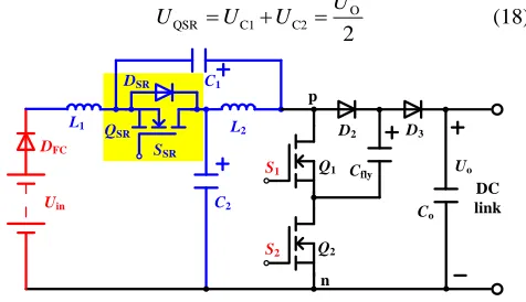
body diode), which is of lower on-resistance. This proposed BTL-SRqZ for the fuel cell vehicles is shown in Fig. 5. The voltage stress of QSR is also half the output voltage as follows
when S1S2=11
O
QSR C1 C2
2 U
U U U (18)
Uin L1
DSR
L2
C1
C2
DFC
D2 D3
Cfly
Co S1
S2
Uo DC link QSR
Q1
Q2 SSR
n p
Fig. 5 Proposed Boost three-level DC-DC converter with synchronous rectification quasi-Z source (BTL-SRqZ) for fuel cell vehicles.
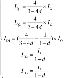
As to the gate driving signal SSR for the synchronous
rectification power switch QSR, it can be obtained from
"Exclusive OR" logic combining S1 and S2 depicted in Fig.
6(a~d). In order to avoid conduction behavior of QSR during the
state of S1S2=11, the dead time td must be added to the ideal gate
driving signal of QSR, by the principle of "OFF in advance, and
ON with delay" as shown in Fig. 6(b~d). For instance, QSR must
be turned off ahead of time by td before the switching state
changes to S1S2=11, and turned on with delayed time td after
S1S2 is changed to 01 or 10. In addition, td is determined by the
dead time modulation index md and carrier period T easily as
follows, shown in Fig. 6(a, d)
d d
2 T
t m (19)
The anti-parallel body diode DSR conducts when QSR is turned
off in advance, and the current flows through DSR instead of QSR.
As a result, the voltage stress of QSR is just the forward voltage
drop of DSR, i.e. QSR is turned off with near Zero-Voltage
Switching (ZVS), as shown in Fig. 6(d~f). Similarly, QSR is
turned on with ZVS.
S1
S2
T
T/2
(b)
(c) 1
0 11 01
0
1 11 10
SSR
(d)
td
0.5
carrier2 carrier1
T/2 0
m
1
(a) (m+md)
T td
0
shift shift
iDSR
UQSR
(e)
(f)
Uo/2
ZVS
[image:5.612.327.548.122.303.2]trun-off trun-onZVS
Fig. 6 Gate driving signals of synchronous rectification power switches, dead time and zero-voltage switching.
IV. COMPONENT PARAMETERS DESIGN
A. Power switches and diodes
From (10) and (14), it is shown that the voltage UCfly of the
flying capacitor Cfly is half of the output voltage UO, as well as
the total voltage of C1 and C2. The voltage stress of the power
switches and diodes employed in the proposed topology can be deduced in terms of the energy flow paths among the voltage source, inductors and capacitors during their effective switching states as shown in Fig. 2. When S1S2=01, Q1 and D3 are in the
OFF state as shown in Fig. 2(a). Therefore, the blocking voltages of Q1 and D3 are UCfly and (UOUCfly), respectively.
When S1S2=10, Q2 and D2 are turned off as shown in Fig. 2(b).
So, the voltage stresses of Q2 and D2 are clamped by (UOUCfly)
and UCfly, respectively. When S1S2=11, D1~D3 are in the OFF
state as shown in Fig. 2(c). As a result, the blocking voltages of D1~D3 are (UC1+UC2), UCfly and (UO UCfly), respectively.
Stated thus, the voltage stresses of all semiconductors are obtained as follows
O
Q1 Cfly
O
Q2 O Cfly
O
D1 C1 C2
O
D2 Cfly
O
D3 O Cfly
= 2
2
2
2
2 U
U U
U
U U U
U
U U U
U
U U
U
U U U
(20)
With regard to current stresses (namely average currents in the ON state) of the semiconductors Q1, Q2, D1~D3, they can be
[image:5.612.59.297.407.544.2] [image:5.612.393.491.559.687.2]voltage source, inductors and capacitors in the effective switching states as shown in Fig. 2.
Q1 O Q2 O D1 O O D2 O D3 4 3 4 4 3 4 4 1 ( )
3 4 1
1 1 I I d I I d I I d d I I d I I d (21)
where IQ1, IQ2, and ID1~ID3 are average currents of Q1, Q2, and
D1~D3 when they are in the ON state respectively, and IO is the
output load current. In addition, the current stress of DFC is the
average current of the inductor L1, namely
DFC L1 O
2 3 4
I I I
d
(22) It is noted that when S1S2=10 and 01, the current stresses of Q1
and Q2 are lower, (they are the same as the current stresses of D3
and D2 respectively as described in (21)), while they are as high
as double the average currents of the inductors i.e. 4 O
3 4 dI
when S1S2=11.
B. Inductors and capacitors
According to the charging and discharging states of the inductors L1 and L2 as shown in Fig. 3(b~e), L1 and L2 are in the
charging state when S1S2=11. The inductances of L1 and L2 can
be deduced as (23)
C1 i n
1 L1 s C2 2 L2 s 1 2 1 2 U U L d i f U L d i f
(2 )
(2 )
(23)
where iL1 and iL2 are the current fluctuations of L1 and L2,
and fs is the switching frequency. Combining (23) with (9) and
(10), the inductances of L1 and L2 can be obtained as (24), which
relates the output voltage UO, the inductor current fluctuations
L1
i
and iL2, the switching frequency fs, and the duty cycle d
O 1 L1 s O 2 L2 s 1 1 2 1 1 2 U
L d d
i f
U
L d d
i f
(2 )( )
(2 )( )
(24)
When S1S2=11, C1 and C2 are in the discharging state, the
capacitances of C1 and C2 can be deduced as (25), in terms of
Fig. 2(c) and Fig. 3(b~g)
O 1 C1 s O 2 C2 s (2 1)
(3 4 )
(2 1)
(3 4 )
d I
C
d U f
d I
C
d U f
(25)
where UC1 and UC2 are the capacitor voltage fluctuations
of C1 and C2. Regarding the flying capacitor Cfly, it is discharged
when S1S2=10 as shown in Fig. 2(b), and the capacitance of Cfly
can be obtained as
O fly Cfly s I C U f
(26)
where UCfly is the capacitor voltage fluctuation of Cfly, that is
not related with the duty cycle d of power switches. In terms of Fig. 2(b), the output capacitor CO is only charged when S1S2=10;
the capacitance of CO can be deduced as
O O O s d I C U f
(27)
where UO is the capacitor voltage fluctuation of CO.
C. Comparisons with other step-up solutions
According to the deduced above, the comparisons can be drawn between the proposed and the other step-up solutions as shown in TABLE I. The conventional Boost and three-level Boost DC-DC converters need one inductor respectively, but their ideal voltage-gain of 1/(1-d) is limited due to the effects of parasitic resistance and extreme duty cycles. It is noted that the voltage stress of four semiconductors in the three-level Boost DC-DC converter can be reduced a half comparing with that of the conventional one, due to using two additional semiconductors and one flying capacitor. The high voltage-gain step-up DC-DC converters in [23] and [33] need two inductors respectively. Although six semiconductors are employed in the converter without the snubber circuit in [23], there still exist two diodes with the voltage stress of UO, and its maximum
conversion efficiency is about 92.6%. While a maximum conversion efficiency of the converter in [33] is improved to 94%, three semiconductors and three capacitors are needed. However, the voltage stress of all the semiconductors is between UO/2 and UO, e.g. 3UO/4, rather than UO/2. Regarding the
proposed converter, the number of main components is between those of the converters in [23] and [33], the voltage stress of all the semiconductors is UO/2, and its maximum
conversion efficiency can be 95.66%, which is higher than those in [23] and [33].
V. EXPERIMENTAL RESULTS AND ANALYSIS
In order to verify the feasibility and effectiveness of the proposed BTL-SRqZ for fuel cell vehicles, a scale-down 1.2 kW BTL-SRqZ converter prototype was constructed as shown in Fig. 7. In the experiment, the fuel cell stack source UFC=Uin is
replaced by an adjustable DC voltage source with a range of Uin=60~150V, and the converter voltage loop is controlled by a
TMS320F28335 DSP. The power circuit IXTK102N30P MOSFETs (its rated voltage is 300V, and its rated current is 102A, while the output voltage of the converter is UO=400V),
and DSEC60-03A Schottky Barrier Diodes are used. In addition, the switching frequency is fs=10 kHz, the dead time is td=1μs,
the initial values of the qZ source inductors are L1=228μH and
L2=225μH respectively, the load resistor is RL=133~400,
[image:6.612.129.238.77.209.2]TABLE I Comparisons between proposed and other step-up solutions.
Step-up Solutions Voltage Gain Amount of Semiconductors
Amount of Inductors
Amount of Capacitors
Voltage
Stress Current Stress
Maximum Efficiency
Conventional Boost
1 1d ,
(0< d <1)
2 1 1 UO O
1
1dI -
Three-level Boost
1 1d ,
(0< d <1)
4 1 2 O
2
U
O 1
1dI -
Converter without snubber in [23]
2 1d ,
(0< d <1)
6 2 3 O
2
U
, UO O
1.5
1dI , O
0.5
1dI 92.6%
Converter in [33]
2(1 )
1 2
d d
,
(0< d <0.5)
3 2 3 O
2(1 )
U d
O 1 (1 2 )I
d d ,
O 2
1 2 dI , O
1
I d
94%
Proposed converter
2 3 4 d,
(0.5<= d <0.75)
5 2 4 O
2
U
O 4 3 4 dI ,
O 1
(3 4 )(1 d d)I , O 1 1dI
[image:7.612.44.283.112.586.2]95.66%
TABLE II Main experimental parameters of proposed converter.
Parameters and components Values (units)
Rated power Pn 1.2kW
Input dc voltage Uin 60~150V
Output dc voltage UO 400V
Switching frequency fs 10kHz
Dead time td 1μs
Inductor L1 228 μH
Inductor L2 225 μH
Capacitors C1, C2, Cfly 450V/660 μF
Capacitor CO 450V/440 μF
Load RL 133~400
MOSFETs Q1, Q2, QSR IXTK102N30P (300V/102A)
Diodes D2, D3, DFC DSEC60-03A (300V/60A)
Fig. 7 Experimental prototype.
Even when the input voltage is Uin=40V, the experimental
PWM voltage Upn is shown in Fig. 8, and the frequency of Upn is
double of the switching frequency. Although the step-up voltage-gain (UO/Uin) is 10, the actual duty cycles
(d=d1=d2=1-0.3=0.7) are about 0.7, instead of the actual
extreme value of the typical boost converter, which is more than 0.9 under the action of the voltage control loop. Furthermore, the amplitude of Upn is 200V (alternating with the
flying-capacitor voltage UCfly and UOUCfly), namely half the
output voltage. Thus, it verifies UCfly=UO/2 in the steady state,
and the flying-capacitor voltage self-balances well without any extra controls.
(10μs/div)
t
Uin=40V
(10V/div)
Upn (50V/div)
UCfly=200V UO-UCfly=200V
/ 2 50μs
T
1
(1 )
30μs
d T
[image:7.612.334.543.572.708.2]Half switching period
Fig. 8 Output PWM voltage when input voltage Uin=40V and M=10.
The experimental results of the synchronous rectification ZVS for the SRqZ source system are shown in Fig. 9. Because of the dead time td=1μs, QSR is bound to be turned on with a
delay, and the anti-parallel body diode DSR is conducted during
the dead time. It is noticed that the voltage stress of QSR changes
from the forward voltage drop of DSR to half the output voltage
during the dead time. Therefore, QSR can be turned off with ZVS,
as shown in Fig. 9. Similarly, the voltage stress of QSR changes
from half the output voltage to the forward voltage drop of DSR
during the dead time. Thus, QSR can be turned on with ZVS.
(4μs/div) t
UGS (5V/div)
UDS (50V/div)
ZVS Turn-off
ZVS Turn-on
Fig. 9 Experimental results of synchronous rectification ZVS.
cell vehicles, the experimental results, in which the input voltage Uin is changed gradually from the wide range of 120V to
40V over dozens of seconds are shown in Fig. 10(a). It is seen that the output voltage UO nearly stays around the reference
voltage 400V under the action of the voltage control loop, and the wide step-up voltage-gain (UO/Uin) range changes from 3.3
to 10. In fact, the actual voltage-gain in the voltage control loop is more than 3.3 to 10 due to the losses compensation of the converter's operation. Correspondingly, the input current (iL1)
increases gradually with the wide-range changed input voltage (from 120V to 40V), as shown in Fig. 10(b), when the load is constant.
Uin=120V~40V
(20V/div) 120V
40V
Uo=400V
(100V/div)
t(4s/div)
(a)
Uin=120V~40V
(20V/div) 120V
iL1(5A/div)
t(4s/div)
40V
(b)
Fig. 10 Output voltage and inductor current with wide-range changed input voltage from 120V to 40V in dynamic state. (a) Output and input voltages. (b) Input current and voltage.
In Fig. 11, the flying-capacitor voltage UCfly is changed
according to the output voltage UO (between 200V and 400V in
the open loop) in the static and dynamic states. It is noticed that the flying-capacitor voltage UCfly still keeps at half of the output
voltage UO, especially in the dynamic states I and II. Because
the voltage across the flying-capacitor is clamped by the total voltages of the qZ source capacitors, whose voltages are related to the corresponding real-time duty cycles and the output voltage UO.
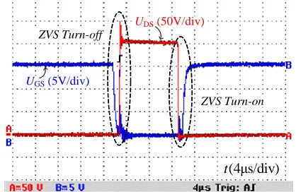
Under the voltage control loop, the proposed BTL-SRqZ converter operates well in conditions of the output voltage UO=400V, and the output power PO=1.2 kW. The output PWM
voltage Upn and the inductor current iL1 are shown in Fig. 12(a).
The inductor L1 is charged when the instantaneous PWM
voltage of Upn is zero (S1S2=11). Then the inductor L1 is
discharged when Upn stays at UO/2=200V (S1S2=01 or 10). In
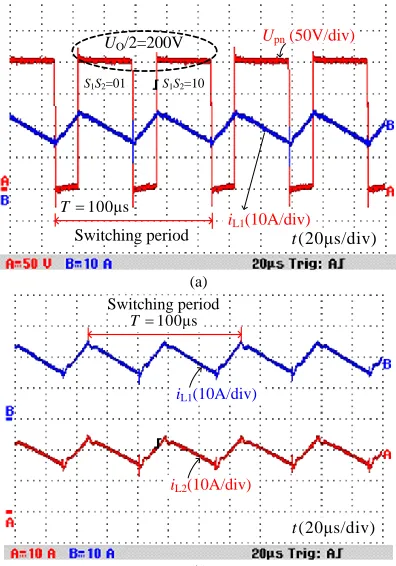
addition, the current iL2 of the inductor L2 is nearly the same as
that of L1, as shown in Fig. 12(b). Therefore, the inductors of the
UO (100V/div)
400V
200V 200V
UCfly (50V/div)
100V
In static state In dynamic
State I
In dynamic State II
[image:8.612.339.545.48.192.2] [image:8.612.68.278.191.495.2]t(4s/div)
Fig. 11 Dynamic flying capacitor voltage corresponding to the variable output voltage UO=200~400V in open loop.
qZ source are charged and discharged twice during each switching period. Compared with the converter in [33], there are one additional active power switch and two more diodes in the proposed converter. However, the equivalent switching frequency of the proposed converter is double the one of the converter in [33]. All the volumes of capacitors and inductors in the quasi-Z-source can be reduced by almost a half compared with those of the converter in [33]. In addition, the quasi-Z-source capacitor voltage stresses are lower than those of the converter in [33]. Therefore, the volume of the proposed converter can be significantly reduced compared to that of the converter in [33].
Upn (50V/div)
iL1(10A/div)
(20μs/div)
t 100μs
T
Switching period
UO/2=200V
S1S2=01 S1S2=10
(a)
(20μs/div)
t
iL2(10A/div)
iL1(10A/div) 100μs
T
Switching period
[image:8.612.340.538.358.641.2](b)
Fig. 12 Output PWM voltage and inductor currents. (a) Output PWM voltage and inductor current. (b) Inductor currents.
In order to validate the dynamic behavior of the proposed converter, an experiment was carried out which used a step change of load between 133Ω and 200Ω, and the output voltage and inductor current are shown in Fig. 13. The inductor currents (e.g. iL1) have corresponding responses between 8A and 12A,
the voltage loop. It can be seen that iL1 changes to 12A from 8A
over 20ms with the load step-change from 200Ω to 133Ω, and it recovers from 12A to 8A over 20ms with the load step-change from 133Ω to 200Ω.
UO(100V/div)
iL1(5A/div)
Load step-change from 200 Ω to 133Ω
Load step-change from 133 Ω to 200Ω
t(100ms/div)
Fig. 13 Output voltage and inductor current when load step-change between 133Ω and 200Ω.
For the wide input-voltage range operation of the proposed converter, the conversion efficiencies related to the variable input voltages (e.g. 60V, 80V, ···, 140V, 150V) and the different output powers (e.g. 400W, 800W, 1200W) are measured by a Power Analyzer (Yokogawa-WT3000). Then, the relationship between the efficiency, the variable input voltages and the different output powers in SR operation are illustrated in Fig. 14. It is noticed that the maximum measured efficiency in SR operation is about 95.66% as shown in Fig. 14. In addition, when the output power is constant and the input voltage declines, the efficiency decreases correspondingly, due to the increasing losses caused by the growing input current. In the same conditions above, the efficiencies in DR operation are also measured, and the SR efficiency is higher than that of DR. The minimum efficiency difference area appears around the medium input voltage (Uin=120V), and its average efficiency
difference is about 0.6%. While the maximum efficiency difference area exists around the lower and higher input voltage (Uin=80V and 150V) areas, and its average value is near 0.85%.
86 88 90 92 94 96
E
ff
ic
ie
n
cy
(
%
)
[image:9.612.66.280.98.237.2]60 80 100 120 140 150 Uin (V)
Fig. 14 Relationship between efficiency, variable input voltages and different output powers in SR operation.
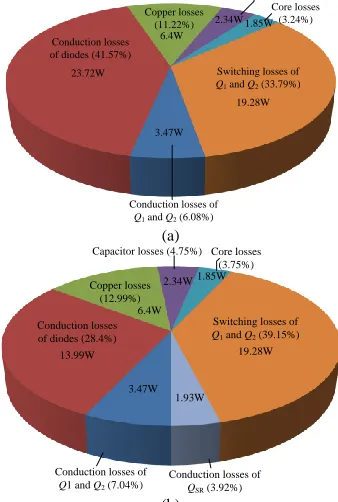
The calculated loss distributions for the experiment when Uin=150V and PO=1200W are shown in Fig. 15. In DR
operation, the total losses of the converter are 57.06W, and the loss distribution is shown in Fig. 15(a). The turn-on and turn-off (switching) and conduction losses of Q1 and Q2 account for
39.87% of the total losses. The conduction losses of all diodes D1-D3 and DFC account for 41.57% of the total losses, which is a
little more than the switching and conduction losses of Q1 and
Q2, due to the higher conduction loss of D1 (in the
quasi-Z-source). However, the total losses of the converter are reduced to 49.26W in the SR operation, and the loss distribution is shown in Fig. 15(b). The switching and conduction losses of Q1 and Q2 account for 46.19% of the total losses, and the
conduction losses of D2, D3, DFC and QSR are reduced to 32.32%
of the total losses due to the SR operation of QSR, instead of D1
in the quasi-Z-source.
PQ PD Pcu PC Pfe P2 Conduction losses
of diodes (41.57%)
Conduction losses of Q1 and Q2 (6.08%)
Switching losses of Q1 and Q2 (33.79%) Copper losses
(11.22%)
Core losses (3.24%) Capacitor losses (4.1%)
3.47W 23.72W
6.4W
2.34W 1.85W
19.28W
(a)
PQ PDSR Pcu PC Pfe P2 PQSR
Conduction losses of diodes (28.4%)
Conduction losses of
Q1 and Q2 (7.04%)
Switching losses of
Q1 and Q2 (39.15%)
Copper losses (12.99%)
Core losses (3.75%) Capacitor losses (4.75%)
3.47W 13.99W
6.4W 2.34W1.85W
19.28W
Conduction losses of
QSR (3.92%) 1.93W
(b)
Fig. 15 Calculated loss distributions for experiment when Uin=150V and
PO=1200W. (a) In DR operation. (b) In SR operation.
VI. CONCLUSION
The topology of the BTL-SRqZ is proposed in this paper. It has the advantages of lower voltage stress for the power semiconductors and the common ground between the input and output sides, as well as the wider range of the voltage-gain with modest duty cycles
0.5, 0.75
for the power switches. Inaddition, the voltage of the flying-capacitor can be clamped well at half the output voltage by the capacitor voltages of the quasi-Z source net in both the static and dynamic states. At the same time, the synchronous rectification power switch operates with ZVS turn-on and turn-off, and the losses of the quasi-Z source circuit can be reduced by the synchronous rectification operation. Therefore, it is suitable to vehicles powered by a fuel cell stack which has a soft output characteristic.
REFERENCES
[1] C. Jin, X. Sheng, and P. Ghosh, “Optimized electric vehicle charging with intermittent renewable energy sources,” IEEE Journal of Selected Topics in Signal Processing, vol. 8, no. 6, pp. 1063–1072, Dec. 2014. [2] B. Zeng, J. Zhang, X. Yang, J. Wang, J. Dong, and Y. Zhang, “Integrated
planning for transition to low-carbon distribution system with renewable energy generation and demand response,” IEEE Trans. Power Syst., vol. 29, no. 3, pp. 1153–1165, May 2014.
[image:9.612.354.523.141.392.2] [image:9.612.61.287.487.606.2][4] K. Li, T. Chen, Y. Luo, and J. Wang, “Intelligent environment-friendly vehicles: concept and case studies,” IEEE Trans. Intelligent Transportation Systems, vol. 13, no. 1, pp. 318–328, Mar. 2012. [5] A. T-Raissi, and D. L. Block, “Hydrogen: automotive fuel of the future,”
IEEE Power & Energy Magazine, vol. 2, no. 6, pp. 40–45, Nov. 2004. [6] A. S. Samosir, and A. H. M. Yatim, “Implementation of dynamic
evolution control of bidirectional DC–DC converter for interfacing ultracapacitor energy storage to fuel-cell system,” IEEE Trans. Ind. Electron., vol. 57, no. 10, pp. 3468–3473, Oct. 2010.
[7] G. Fontes, C. Turpin, and S. Astier, “A Large-signal and dynamic circuit model of a H2/O2 PEM fuel cell: description, parameter identification,
and exploitation,” IEEE Trans. Ind. Electron., vol. 57, no. 6, pp. 1874–1881, Jun. 2010.
[8] A. Askarzadeh, and A. Rezazadeh, “An innovative global harmony search algorithm for parameter identification of a PEM fuel cell model,” IEEE Trans. Ind. Electron., vol. 59, no. 9, pp. 3473–3480, Sep. 2012. [9] J. Morales-Morales, I. Cervantes, and U. Cano-Castillo, “On the design of
robust energy management strategies for FCHEV,” IEEE Trans.Veh. Technol., vol. 64, no. 5, pp. 1716–1728, May 2015.
[10] G. Su, and L. Tang, “A reduced-part, triple-voltage DC–DC converter for EV/HEV power management,” IEEE Trans. Power Electron., vol. 24, no. 10, pp. 2406–2410, Oct. 2009.
[11] U. R. Prasanna, and A. K. Rathore, “Dual three-pulse modulation-based high-frequency pulsating DC link two-stage three-phase inverter for electric/hybrid/fuel cell vehicles applications,” IEEE Journal of Emerging and Selected Topics in Power Electronics, vol. 2, no. 3, pp. 477–486, Oct. 2014.
[12] J. Jia, G. Wang, Y. T. Cham, Y. Wang, and M. Han, “Electrical characteristic study of a hybrid PEMFC and ultracapacitor system,” IEEE Trans. Ind. Electron., vol. 57, no. 6, pp. 1945–1953, Dec. 2010. [13] N. D. Benavides, and P. L. Chapman, “Mass-optimal design methodology
for DC-DC converters in low-power portable fuel cell applications,”
IEEE Trans. Power Electron., vol. 23, no. 3, pp. 1545–1555, May 2008. [14] G. Dotelli, R. Ferrero, P. G. Stampino, S. Latorrata, and S. Toscani, “PEM fuel cell drying and flooding diagnosis with signals injected by a power converter,” IEEE Trans. Instrum. Meas., vol. 64, no. 8, pp. 2064–2071, Aug. 2015.
[15] S. Dusmez, A. Hasanzadeh, and A. Khaligh, “Comparative analysis of bidirectional three-level DC–DC converter for automotive applications,”
IEEE Trans. Ind. Electron., vol. 62, no. 5, pp. 1063–1072, May 2015. [16] H. Chen, and J. Liao, “Design and implementation of sensorless capacitor
voltage balancing control for three-level Boosting PFC,” IEEE Trans. Power Electron., vol. 29, no. 7, pp. 3808–3817, Jul. 2014.
[17] X. Ruan, B. Li, Q. Chen, S. Tan, and C. K. Tse, “Fundamental considerations of three-level DC–DC converters: topologies, analyses, and control,” IEEE Trans. Circuits Syst. I, Reg. Papers, vol. 55, no. 11, pp. 3733–3743, Dec. 2008.
[18] L. Shi, B. P. Baddipadiga, M. Ferdowsi, and M. L. Crow, “Improving the dynamic response of a flying-capacitor three-level Buck converter,” IEEE Trans. Power Electron., vol. 28, no. 5, pp. 2356–2365, May 2013. [19] Y. J. A. Alcazar, D. S. Oliveira, Jr., F. L. Tofoli, and R. P.
Torrico-Bascopé, “DC–DC nonisolated Boost converter based on the three-state switching cell and voltage multiplier cells,” IEEE Trans. Ind. Electron., vol. 60, no. 10, pp. 4438–4449, Oct. 2013.
[20] Y. Tang, D. Fu, T. Wang, and Z. Xu, “Hybrid switched-inductor converters for high step-up conversion,” IEEE Trans. Ind. Electron., vol. 62, no. 3, pp. 1480–1490, Mar. 2015.
[21] W. Qian, D. Cao, J. G. Cintrón-Rivera, M. Gebben, D. Wey, and F. Z. Peng, “A switched-capacitor DC–DC converter with high voltage gain and reduced component rating and count,” IEEE Trans. Ind. Appl., vol. 48, no. 4, pp. 1397–1406, Jul./Aug. 2012.
[22] A. M. Jorge, L. Rodrigo, P. Elvia, and L. G. Jorge, “Modelling and control of a DC–DC quadratic boost converter with R2P2,” IET Power Electron., vol. 7, no. 1, pp. 11–22, May 2014.
[23] R. Gules, L. L. Pfitscher, and L. C. Franco, “An interleaved Boost DC-DC converter with large conversion ratio,” ISIE'03, pp. 411–416, Jun. 2003. [24] Q. Zhao, and F. C. Lee, “High-efficiency, high step-up DC–DC converters,” IEEE Trans. Power Electron., vol. 18, no. 1, pp. 65–73, Jan. 2003.
[25] G. A. L. Henn, R. N. A. L. Silva, P. P. Praça, L. H. S. C. Barreto, and D. S. Oliveira, “Interleaved-Boost converter with high voltage gain,” IEEE Trans. Power Electron., vol. 25, no. 11, pp. 2753–2761, Nov. 2010.
[26] P. P. Praça, G. A. L. Henn, D. S. Oliveira, L. H. S. C. Barreto, and R. N. A. L. Silva, “High voltage gain single stage DC-DC converter based on three-state commutation cell,” APEC'13, pp. 2882–2887, Mar. 2013. [27] S. J. Amodeo, H. G. Chiacchiarini, and A. R. Oliva, “High-performance
control of a DC–DC Z-source converter used for an excitation field driver,” IEEE Trans. Power Electron., vol. 27, no. 6, pp. 2947–2957, Jun. 2012.
[28] V. P. Galigekere and M. K. Kazimierczuk, “Analysis of PWM Z-source DC-DC converter in CCM for steady state,” IEEE Trans. Circuits Syst. I, Reg. Papers, vol. 59, no. 4, pp. 854–863, Apr. 2012.
[29] S. Yang, F. Z. Peng, Q. Lei, R. Inoshita, and Z. Qian, “Current-fed quasi-Z-source inverter with voltage Buck–Boost and regeneration capability,” IEEE Trans. Ind. Appl., vol. 47, no. 2, pp. 882–892, Mar./Apr. 2011.
[30] O. Ellabban, H. Abu-Rub, and B. Ge, “A quasi-Z-source direct matrix converter feeding a vector controlled induction motor drive,” IEEE Journal of Emerging and Selected Topics in Power Electronics, vol. 3, no. 2, pp. 1063–1072, Jun. 2015.
[31] K. Patidar, and A. C. Umarikar, “High step-up pulse-width modulation DC–DC converter based on quasi-Z-source topology,” IET Power Electron., vol. 8, no. 4, pp. 477–488, 2015.
[32] B. Poorali, A. Torkan, and E. Adib, “High step-up Z-source DC–DC converter with coupled inductors and switched capacitor cell,” IET Power Electron., vol. 8, no. 8, pp. 1394–1402, 2015.
[33] H. Shen, B. Zhang, D. Qiu, and L. Zhou, “A common grounded Z-source DC-DC converter with high voltage gain,” IEEE Trans. Ind. Electron., vol. 63, no. 5, pp. 2925–2935, 2016.
Yun Zhang (M’13) was born in Jiangsu, China, in 1980. He received the B.S. and M.S. degrees in electrical engineering from the Harbin University of Science and Technology, Harbin, China, in 2003 and 2006, respectively, and the Ph.D. degree in electrical engineering from the Harbin Institute of Technology, Harbin, in 2010.
He is currently an Associate Professor at the School of Electrical Engineering and Automation, Tianjin University, Tianjin, China. His current research interests include topologies, modulation, and control strategies of power converters for microgrid and electric vehicles.
Jilong Shi was born in Shandong, China. He received his B.S. degree in Electrical Engineering from the Changchun University Of Science and Technology, Changchun, China, in 2014. He started pursing his M.S. degree in Electrical Engineering from Tianjin University, Tianjin, China, in 2014. His current research interests include DC-DC converters, and fuel cell vehicles.
Jing Li (M’15) received the B.Eng. (Hons.) and M.Sc. (Distinction) degrees from the Beijing Institute of Technology, Beijing, China, in 1999, and 2002, respectively, and the Ph.D. degree from the University of Nottingham, Nottingham, U.K., in 2010.
She was a Research Fellow with the Power Electronic, Machine and Control Group, University of Nottingham. She is currently a Lecturer at the Department of Electrical and Electronic Engineering, University of Nottingham, Ningbo, China. Her research interests include condition monitoring for motor drive systems and power distribution systems and advanced control and design of motor drive systems.
Mark Sumner (SM’05) received the B.Eng. degree in electrical and electronic engineering from Leeds University, Leeds, U.K., in 1986, and the Ph.D. degree in induction motor drives from the University of Nottingham, Nottingham, U.K., in 1992.
He was with Rolls Royce, Ltd., Ansty, U.K. He was a Research Assistant with the University of Nottingham, where he became a Lecturer in October 1992, and is currently a Professor of electrical energy systems. His research interests include control of power electronic systems including sensorlessmotor drives, diagnostics and prognostics for drive systems, power electronics for enhanced power quality, and novel power system fault location strategies.
Ping Wang was born in Tianjin, China, in 1959. She received the B.S., M.S., and Ph.D.degrees in Electrical Engineering from the Tianjin University, Tianjin, China, in 1981, 1991, and 2005, respectively. Since 1981, she has been a Teacher and a Researcher at Tianjin University, where she is currrently a Professor.
Her current research interests include power electronic control of renewable energy sources, PWM converters, and intelligent detection and control.
Changliang Xia (M’08-SM’12) was born in Tianjin, China, in 1968. He received the B.S. degree from Tianjin University, China, in 1990, and the M.S. and Ph.D. degrees from Zhejiang University, China, in 1993 and 1995 respectively, all in electrical engineering.
![Fig. 4 Comparison of voltage-gain M via duty cycles d among conventional Boost three-level converter, interleaved converter in [23], common ground converter in [33], and proposed one](https://thumb-us.123doks.com/thumbv2/123dok_us/8592496.371198/4.612.71.275.54.389/comparison-voltage-conventional-converter-interleaved-converter-converter-proposed.webp)