Efficient modular multilevel converter based on
active-forced-commutated hybrid packed u-cells for HV networks
Ahmed Darwish*
*Lancaster University, United Kindgom, [email protected]
Keywords: Voltage source converter (VSC), Modular Multilevel Converter (MMC), Active forced commutation (AFC), High-voltage DC (HVDC) converters.
Abstract
High-voltage DC (HVDC) converter topologies have been more desirable in the off-shore wind energy applications to increase the efficiency and reduce the losses. In this context, the paper presents a modified structure for modular multilevel voltage source converter (VSC) topology where the conduction and switching losses can be significantly reduced. As the conduction losses of the semiconductor devices affect the total efficiency of such systems, replacing part of the Insulated Gate Bipolar Transistor (IGBT) devices with thyristors in the conduction path of the proposed topology can reduce the total losses in the normal operation. Thus, both IGBTs and thyristors are implemented in a hybrid configuration. In this configuration, the IGBT devices are responsible for voltage/current transitions between the positive and negative parts of the waveforms while the thyristor devices are responsible for conducting the currents in the other constant polarity regions. MATLAB simulations and scaled-down experiments show that the modified structure can reduce the total losses of the HVDC converter significantly.
1 Introduction
Due to the recent significant development of the renewable energy sources, such as wind energy systems, High-voltage DC (HVDC) converter topologies become very vital [1,2]. This comes from the fact that HVDC converters, operating with Insulated Gate Bipolar Transistor (IGBT) switches, have several merits such as: (i) the ability to generate output or intermediate voltages and currents with low harmonic content, (ii) the possibility of decoupled active and reactive power control, (iii) system’s modularity and (iv) scalability and redundancy [3]–[5]. When the MMC is coupled with a low or medium frequency transformer, the dv/dt applied on the transformers’ windings can be reduced significantly [6]. However, because of their very low power losses, thyristor-based Line Commutated Converters (LCC) are still dominant in high-voltage/high-power applications. To give an indication for that, the typical forward voltage of the 4.4kV/1.2kA Infineon FZ1200R45KL3_B5 IGBT is 3V while
The description and MATLAB simulations of the three-phase dc-ac mode will be presented in Section 4. The dc-dc operation of the system will be shown in Section 4. Section 5 shows the experimental results of the scaled-down prototype to validate the basic principle of the system while the conclusion will be summarized in Section 6.
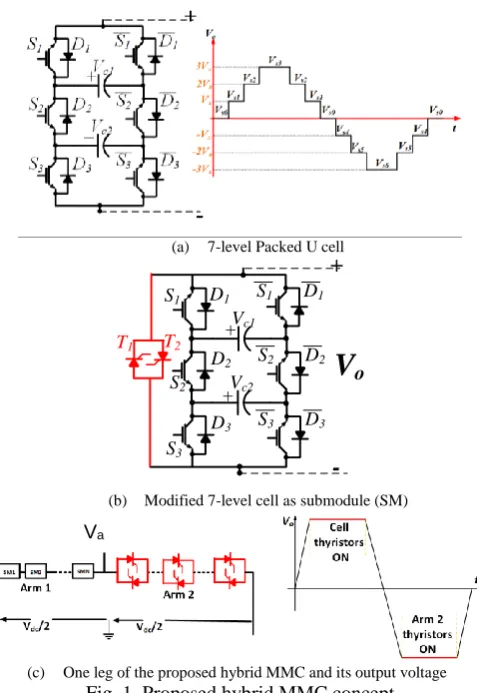
(a) 7-level Packed U cell
D1 S1 D1
D2 S2 D2
D3 S3 D3
Vc1
+
Vc2
+
+
T1
V
o-T2
S1
S2
S3
(b) Modified 7-level cell as submodule (SM)
(c) One leg of the proposed hybrid MMC and its output voltage Fig. 1. Proposed hybrid MMC concept
2 Operation principle
As stated earlier, the PUC can generate seven voltage levels. This section explains the operation principle for the proposed MMC with one cell per arm per phase. In this case, the switching states of the cell are listed in Table 1.
State T1 T2 S1 S2 S3 Vo
St1 OFF OFF 1 0 0 Vdc/N
St2 OFF OFF 1 0 1 2Vdc/3N
St3 OFF OFF 1 1 0 Vdc/3N
St4 ON ON 0 0 0 0
St5 OFF OFF 0 0 1 -Vdc/3N
St6 OFF OFF 0 1 0 -2Vdc/3N
[image:2.595.311.551.88.259.2]St7 OFF OFF 0 1 1 -Vdc/N
Table 1: Switching states.
Fig. 2 shows the simplified operation when only one cell is inserter in Arm 1 of each phase (N=1). During the transition
period (tr), the PUC in Arm 1 is switching its states in order to
[image:2.595.47.286.159.506.2]change its terminal voltage from zero to Vdc as shown in
Table 1. Meanwhile, the phase voltage (Va) is switching from
its positive half cycle value (Van = Vdc/2) to the negative half
cycle (Van = -Vdc/2). In this way, the IGBTs of each cell are
switching and conducting in very short duration which is the transition period while the thyristor are responsible for conducting the currents in all other durations. Because the cells are able to generate voltage with different polarities, the negative voltages are used to turn of the cell thyristors (T1 and
T2). In the normal operation where Arm 1 has numerous cells,
redundant cells NR are responsible to generate additional
voltage to Arm 1 in order to turn off the thyristors of Arm 1 when required. These redundant cells can be of PUC type or of the conventional HB cells. Their role will be to provide an additional voltage during a short duration (toff1) to ensure
turning off the thyristors of Arm 2 if the current is passing through Arm 2 thyristors from up to down. If the current is passing in the opposite direction, one or some of Arm 1 cells will produce negative voltage on its terminals in order to turn Arm 2 thyristors off. This will be repeated to turn off Arm 1 cell thyristors according to the current direction in the cells. Because the thyristors are ON for relatively long time durations, the cell capacitors of the PUC can be charged using the redundant states of the cells by the knowledge of the current polarity and capacitors voltage values [9].
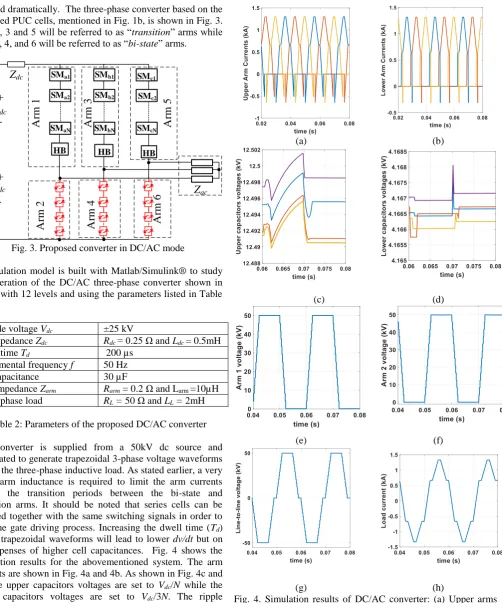
3 DC/AC converter
The trapezoidal voltage modulation concept of the dc/dc converter, shown in Fig. 2, has been proposed in [6] as an efficient alternative for HVDC systems. As stated earlier, the converter size can be significantly reduced according to the smaller capacitances required. Although the trapezoidal waveform has higher harmonic content, this can be eliminated by using Selective Harmonic Elimination (SHE) modulation technique and/or the installation of line filters to meet the grid standards. In this system, the arm inductances are only needed when the lower thyristor (Arm 2) arm is ON. Thus, no or very small arm inductances can be used in the said trapezoidal mode of operation and therefore the converter size can be
St3
St4 St2 St1 St2St3 St4
Arm 2 Thyristors ON
tr tr
T1 and T2 ON
Arm 1 cell voltage Vo Vdc
2/3Vdc
1/3Vdc
Vdc/2
Vdc/6
-Vdc/6
-Vdc/2
toff1
t
Phase voltage Va
toff2 Td
Fig. 2. Operation of the proposed converter
[image:2.595.37.296.602.703.2]reduced dramatically. The three-phase converter based on the modified PUC cells, mentioned in Fig. 1b, is shown in Fig. 3. Arm 1, 3 and 5 will be referred to as “transition” arms while
Arm 2, 4, and 6 will be referred to as “bi-state” arms.
A
rm
6
A
rm
4
½
V
dc½
V
dcZ
dc SMa1SMa2
SMaN
SMb1
SMb2
SMbN
SMc1
SMc2
SMcN
HB HB HB
Z
acA
rm
1
A
rm
3
A
rm
5
A
rm
2
+
-+
-Fig. 3. Proposed converter in DC/AC mode
A simulation model is built with Matlab/Simulink® to study the operation of the DC/AC three-phase converter shown in Fig. 3 with 12 levels and using the parameters listed in Table 2.
DC side voltage Vdc ±25 kV
DC impedance Zdc Rdc = 0.25 Ω and Ldc= 0.5mH
Dwell time Td 200 µs
Fundamental frequency f 50 Hz
Cell capacitance 30 µF
Arm impedance Zarm Rarm = 0.2 Ω and Larm =10µH
Three-phase load RL = 50 Ω and LL = 2mH
Table 2: Parameters of the proposed DC/AC converter The converter is supplied from a 50kV dc source and modulated to generate trapezoidal 3-phase voltage waveforms across the three-phase inductive load. As stated earlier, a very small arm inductance is required to limit the arm currents during the transition periods between the bi-state and transition arms. It should be noted that series cells can be grouped together with the same switching signals in order to ease the gate driving process. Increasing the dwell time (Td)
of the trapezoidal waveforms will lead to lower dv/dt but on the expenses of higher cell capacitances. Fig. 4 shows the simulation results for the abovementioned system. The arm currents are shown in Fig. 4a and 4b. As shown in Fig. 4c and 4d, the upper capacitors voltages are set to Vdc/N while the
lower capacitors voltages are set to Vdc/3N. The ripple
voltages are within the range of 1% using the conventional sorting technique where the cells are ordered according to their voltages and to the arm current direction. The upper and lower arms voltages are shown in Fig.4e and 4f. Finally, the output phase voltages and load currents are shown in Fig. 4g and 4h.
(a) (b)
(c) (d)
(e) (f)
(g) (h)
Fig. 4. Simulation results of DC/AC converter: (a) Upper arms currents, (b) lower arms currents, (c) upper capacitors voltages of Arm 1, (d) lower capacitors voltages of Arm 1, (e) Arm 1 voltage, (f) Arm 2 voltage, (g) Line-to-line voltage (Vab), and
[image:3.595.69.572.79.683.2] [image:3.595.49.289.140.333.2](a) (b)
(c) (d)
(e) (f)
(g) (h)
Fig. 5. Simulation results of DC/AC converter with SHE modulation: (a) Upper arms currents, (b) lower arms currents, (c) upper capacitors voltages of Arm 1, (d) lower capacitors voltages of Arm 1, (e) Arm 1 voltage, (f) Arm 2 voltage, (g) Line-to-line voltage (Vab), and (h) phase a load current
To reduce the harmonic content of the output voltages and currents, SHE modulation technique can be used. To give an example for that, the results in Fig. 5 show the operation of the DC/AC converter when operating using the SHE modulation to eliminate the fifth harmonic in the output current. Fig. 6 shows the THD of the output current with and without the SHE.
Frequency (Hz) Frequency (Hz)
[image:4.595.57.389.72.679.2](a) (b)
Fig. 6. THD of output current: (a) without SHE and (b) with SHE for fifth harmonic (250 Hz).
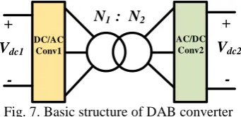
4 DC/DC operation
The proposed topology is more suitable to operate in front-to-front dc-dc transformer and can act as a dual active bridge (DAB) converter [10]. Generally, there are two dc/ac and ac/dc converters connected together via three-phase two-winding transformer at the line frequency as shown in Fig. 7. However, increasing this frequency will lead to a significant reduction in the transformer size. In addition using the trapezoidal waveforms as described in Fig. 1 and Fig. 2 will reduce the dv/dt stresses on the cells and the interfacing transformer and will lead to another significant reduction in the size of submodule cells and therefore the total size of the DAB. Using thyristors in the PUC cells as well as the lower arm is expected to reduce the conduction losses and increase the total efficiency significantly.
DC/AC Conv1
AC/DC Conv2
V
dc1+
-V
dc2+
[image:4.595.344.515.512.595.2]-N
1: N
2Fig. 7. Basic structure of DAB converter
In addition to the DAB operation in Fig. 7, the proposed topology can be used in other HVDC structures such as HVDC auto-transformers. The proposed topology is capable of providing black start following dc grid faults. Because the proposed cells are bidirectional, it is possible to generate the required voltage to block the dc side faults. In addition, the ac-link transformer should be able to prevent fault propagating between the primary and secondary sides. A Simulink/MATLAB model is built for the system in Fig. 7 using the parameters in Table 3.
(a) (b)
(c) (d)
(e) (f)
[image:5.595.275.572.81.658.2](g) (h)
Fig. 8. Simulation results of DAB system (Conv 1): (a) Upper arms currents, (b) lower arms currents, (c) upper capacitors voltages of Arm 1, (d) lower capacitors voltages of Arm 1, (e) Arm 1 voltage, (f) Arm 2 voltage, (g) Line-to-line voltage (Vab), and phase a load current
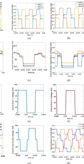
(a) (b)
(c) (d)
(e) (f)
(g) (h)
Fig. 9. Simulation results of DAB system (Conv 2): (a) Upper arms currents, (b) lower arms currents, (c) upper capacitors voltages of Arm 1, (d) lower capacitors voltages of Arm 1, (e) Arm 1 voltage, (f) Arm 2 voltage, (g) Line-to-line voltage (Vab),
[image:5.595.45.294.86.651.2]Side 1 dc voltage Vdc1 ±20 kV
Side 2 dc voltage Vdc2 ±40 kV
DC impedance Zdc Rdc = 0.25 Ω and Ldc= 0.5mH
Dwell time Td 10 µs
Fundamental frequency f 250 Hz
Cell capacitance 30 µF
Arm impedance Zarm Rarm = 0.2 Ω and Larm =10µH
Number of PUC cells per arm N
4
Table 3: Parameters of the proposed DAB system
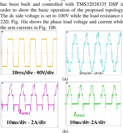
5 Experimental results
A scaled down DC/AC prototype with two cells in each arm has been built and controlled with TMS32028335 DSP in order to show the basic operation of the proposed topology. The dc side voltage is set to 100V while the load resistance is 22Ω. Fig. 10a shows the phase load voltage and current while the arm currents in Fig. 10b.
(a)
(b)
Fig. 10. Experimental results of DC/AC converter: (a) phase load voltage and current and (b) upper and lower arm currents
6 Conclusion
A modified seven-level Packed-U-cell has been used in a hybrid dc/ac topology for HVDC application. The proposed topology can be extended to DAB front-to-front and dc-dc autotransformer configurations. The cells of the upper arm have been modified by adding back-to-back thyristors while the lower arms have been replaced with series back-to-back thyristors to enable generating trapezoidal output voltages at its terminals. Consequently, the conduction losses of the converter can be reduced to half the value of its conventional counter parts. Additionally, the proposed converter is expected to have smaller cell capacitances as well as arm inductances and hence, smaller overall size. The proposed converter has the advantages of low power dissipation experienced in LCC with the same advantages of voltage sourced converters such as bidirectional power flow, black-start operation after dc link fault, and dc fault blocking.
References
[1] N. Flourentzou, V. G. Agelidis, and G. D. Demetriades, “VSC-based HVDC power transmission systems: An overview,” IEEE Trans. Power Electron., vol. 24, no. 3, pp. 592–602, Mar. 2009.
[2] A. A. Elserougi, et al., “A New Protection scheme for HVDC converters against dc-side faults with current suppression capability,” IEEE Trans. on Power Delivery.
vol. 29, no. 4, pp. 1569–1577, Aug. 2014.
[3] L. Zhang, L. Harnefors, and H. P. Nee, “Modeling and control of VSC-HVDC links connected to island systems,” IEEE Trans. Power Syst., vol. 26, no. 2, pp. 783–793, May 2011.
[4] S. Cole and R. Belmans, “Transmission of bulk power,”
IEEE Ind. Electron. Mag., vol. 3, no. 3, pp. 19–24, Sep. 2009.
[5] Y. Li, Z. W. Zhang, C. Rehtanz, L. F. Luo, S. Rüberg, and D. C. Yang, “A new voltage source converter-HVDC transmission system based on an inductive filtering method,” IET Gen. Transm. Distrib., vol. 5, no. 5, pp. 569–576, May 2011.
[6] I. A. Gowaid et al, “Quasi Two-Level Operation of Modular Multilevel Converter for use in a high-power DC transformer with DC fault isolation capability,” IEEE Transactions on Power Electronics, 2015 30 (1), pp. 108-123
[7] I. A. Gowaid et al, “The Transition Arm Multilevel Converter – A Concept for Medium and High Voltage DC-DC Transformers,” IEEE International Conference on Industrial Technology (ICIT), 2015.
[8] H. Vahedi, and K. Al-Haddad, “Real-Time Implementation of a Seven-Level Packed U-Cell Inverter with a Low-Switching-Frequency Voltage Regulator,”
IEEE Transactions on Power Electronics, vol. 31, no. 8 Aug 2016.
[9] G. P. Adam and I. E. Davidson, “Robust and Generic Control of Full-Bridge Modular Multilevel Converter HVDC Transmission Systems,” IEEE Trans on Power Delivery, vol.30, no.6, pp.2468-2476, Dec.2015.
[image:6.595.42.289.256.522.2]