Optoelectronic Properties of GaN-Based Light-Emitting
Diodes with Different Mesa Structures
Xueyun Song1,2, Xianghua Zeng1*, Junbin Zhang1, Yuzhe Jin1, Xiangdong Meng1
1College of Physics & Technology, Yangzhou University, Yangzhou, China; 2Jiangsu Research Center of Engineering and Technol-
ogy for New Photosorce Solid-State Lighting, Yangzhou, China. Email: *[email protected]
Received September 2nd, 2012; revised October 3rd, 2012; accepted November 4th, 2012
ABSTRACT
GaN/InGaN lighting-emitting diodes with different mesa structures are studied. The current-voltage characteristics, light output power, luminous efficiency, and peak wavelength of the GaN/InGaN lighting-emitting diodes with different mesa patterns are compared. It shows that the current-voltage characteristics of the chips with more mesa areas are im- proved greatly by reducing the current crowding. With higher injection current the light output powers of GaN-based LED with more mesa areas are enhanced. And the chips with more P-electrode area have a smaller red shift and a little bit blue shift due to the reduction of the current crowding.
Keywords: GaN-Based Leds; Mesa Structure; Optoelectronic Properties
1. Introduction
With small volume, light weight and long lifetime ad-vantages, GaN-based LED has a wide range of applica-tions, such as automobiles, backlighting, traffic lights, etc. It can be fabricated to white LED by many approaches, and expected to become the new fourth-generation solid- state lighting [1-5]. But most GaN-based LEDs have an insulating sapphire substrate, so their P and N electrodes are on one side, which inevitably produce current crowd- ing effect [6-9] and result in an uneven distribution of current,serious heating effect, lower light extraction efficiency and output power, and severe red shifted peak of emission wavelength [10-13].
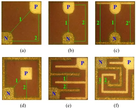
There are many methods to improve the output effi- ciency [14-17], but fabricating GaN-based LEDs with less current crowding has been an objective of research-ers engaged in the filed [6,13]. And it is a good method to reduce the current crowding by optimizing the chip’s electrode which will make the current distribute uni- formly. In Ref [11], they reported on the efficiency of GaN-based LED with different mesa patterns, but they only designed the finger interdigitated patterns. This pa- per reports on the efficiency of GaN-Based LEDs with different mesa structures, here the mesa patterns have a better symmetry and some of them are more complicated (as shown in Figure 1), therefore more results are pre-sented. By comparing the photoelectric parameters of
these samples, such as current-voltage (V-I)characteris- tics, output power, luminous efficiency, peak and domi- nant wavelength, we obtain that the mesa area or the P- electrode area is directly related to the performance of the chips. On the one hand, the chips with more mesa area have a better V-Icharacteristics, on the other hand, as the mesa area will prevent the light emission, the light- emitting efficiency will decrease a little bit smaller, the output power and luminous efficiency are either. There- fore, it needs to compromise between optical and electri- cal properties in order to obtain more favorable optoelec- tronic performance of LEDs.
(a) (b) (c)
[image:1.595.314.532.536.709.2](d) (e) (f)
2. Heterostructure and Chip Design
GaN Based LEDs, which are grown by metal organic chemical vapor (MOCVD) on c-plane (0001)-oriented 2 inch sapphire substrate, consist of a thick undoped GaN buffer layer, an highly conductive n-GaN lower cladding layer, an InGaN/GaN multiple quantum well (MQW) active region, a p-GaN upper cladding and highly doped contact layer. Top-emitting LEDs with size of 356 μm × 356 μm were fabricated using standard photolithography and Cl2/SiCl4/Ar inductively coupled plasma etching for
current isolation purposes. Firstly, the p-GaN and active region were partially etching by an ICP etcher to expose an n-GaN lower cladding layer for electrode formation. Subsequently, a 350 nm thick ITO was deposited on the p-GaN top layer as transparent conductive layer (TCL). And Cr-Au metals were deposited using the electron- beam evaporation system for the P and N electrodes. Fin- ally, SiO2 was deposited as a passive layer to protect
chips by plasma enhanced chemical vapor deposition (PECVD).
The masks make up of the basic unit, and each unit contains six different electrode shapes, each shape with 13 dies. The epitaxial wafer within basic unit size should have a good consistency, so comparing performance of chips with different electrodes are more reasonable with- in the basic unit. For simplicity, the LEDs corresponding to the six mesa patterns are called the samples #1 - #6 in sequence, their corresponding parameters, such as Mesa area, P-electrode area, Light-emitting area, and P-N elec-trodes separation for six samples are presented in Table 1, where the P-N electrodes separation is a typical length between P and N electrode as the labeled number one in
Figure1. The light output power of packaged LEDs was measured in an integrating sphere at constant temperature of T = 298 K in a dc current mode.
[image:2.595.327.518.85.228.2]3. Results
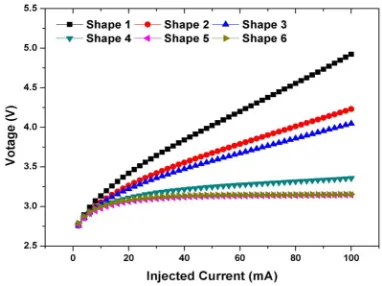
Figure 2 shows the measured voltage-current (V-I) char-
Table 1. The parameters of the Mesa structures. The die size of all LEDs is 356 μm × 356 μm.
Light-emitting area Samples Mesa area P-electrode area
Mesa top Mesa sidewalls
PN electrodes spacing
(μm2) (μm2) (μm2) (μm2) (μm)
#1 115410 9463 105948 1678 221
#2 115084 8925 106159 1911 156
#3 109184 12765 96419 1791 156
#4 86411 10000 76411 1469 107
#5 88233 23510 64723 2737 54
#6 77466 22168 55299 2653 43
Figure 2. V-I characteristics of six samples.
acteristics of the LEDs. For six LEDs (samples #1 - #6),
the forward voltages at 20 mA are 3.419, 3.264, 3.221, 3.110, 3.062, 3.084 V, respectively. With the mesa area increase, at 20 mA the voltages decrease, and the small- est one is 10% lower than the conventional mesa pattern. And the series resistances from the minim value of the derivative in V-I curves are 17.75, 11.12, 9.38, 2.12, 0.25 and 0.13 Ω,respectively, where the last one is only 0.70% of the first. From the separations between P and N electrodes in Table 1, it shows that the smaller the sepa- ration of PN electrodes, and the series resistance will decrease, so the LED V-I characteristics can be improved greatly. As a great current will crowd at the contact elec- trode edges, and results in a non-uniform temperature distribution over the die. This result is consistent with the calculations of Ref [13]. For the latter three mesa pat-terns, the P-contact areas are larger which lead to a small
current density on the P-electrode areas, and the separa-tions between P and N electrodes are smaller which lead to a more uniform current distribution. Comparing the last two mesa patterns, both the separations between P and N electrodes and the P-electrode areas are approxi-mate, so their voltages are almost same. The reason is that the Indium-Tin Oxide (ITO) transparent conductive layer (TCL) which has much better conductivity will spread the current uniformly on its p-type surface, and
[image:2.595.57.288.593.733.2]the effects of the V-I characteristics on the separation and on P-electrode area are small. The voltage-current char-acteristics for latter three kinds of samples are much bet-ter with increasing injection current, and the voltages show saturation with injection current over 30 mA.
powers decrease. At the same time the chips having more uniform current distribution will have a lower forward voltage, therefore input power is relatively lower. But for sample #1 after 60 mA, due to the current crowding ef-fects the light output power decreases.
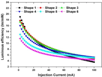
Figure 4 gives the changes of the measured luminous efficiency with injection current for six samples. With increasing injection current, the external quantum effi- ciency drops rapidly, at 20 mA their luminous efficien- cies are 11.37, 11.73, 11.42, 10.35, 8.82 and 7.64l m/mW, respectively. From samples #1 to #6, the luminous effi- ciency decreases gradually, as their top light emitting areas become gradually smaller. But the luminous effi- ciency of sample #1 drops faster than others, because the uneven distributions of the current density induce the current crowding effect, and the thermal effect of the chips will reduce the luminous efficiency at the higher current[12,13]. Therefore, by optimizing mesa structure the luminous efficiency droop at high injection current can be abated.
[image:3.595.330.512.260.384.2]The changes of the peak wavelength with injection current for six samples are shown in Figure 5. With in-creasing injection current, the wavelengths firstly drop down (blue shift), and up to 50 mA reach a minimum, and then increase gradually (red shift). The appearance of the blue or red shift for the peak wavelength may result from the existence of polarization filed in MQWs and heat effect of GaN material [18,19]. Over 50mA a fast
[image:3.595.93.255.432.551.2]Figure 3. Output powers with injection current for six sam-ples.
Figure 4. Luminous efficiencies with injection current for six samples.
Figure 5. Peak wavelengths with injection current for six samples.
Figure 6. Dominant wavelength with injection current for six samples.
[image:3.595.90.254.589.704.2]the chip has less crowding effect, and its heat effect re- duces, the gap shrinks weakly, so the red shift is smaller. The changes of the dominant wavelength are shown in
Figure 6. Similar to the peak wavelength, with increase- ing injection current the dominant wavelengths are blue shift firstly, then red, where the blue shifts are 1.55, 1.5, 1.55, 1.95, 1.85, 1.9 nm,and the red are 6.4, 4.15, 3.35, 2, 1.75, 2.05 nm, respectively.
4. Conclusion
GaN/InGaN lighting-emitting diodes with six mesa struc- tures are studied. For the more mesa area, V-I character- istics of the GaN/InGaN lighting-emitting diodes can be greatly improved by reducing the current crowding. As the chip with more mesa area will countervail the effi-cient light-emitting area, and the light output power will decrease slightly. One can see that with injection current up to 60 mA the light output power of GaN-based LED with more mesa area can be improved greatly. Therefore, this mesa pattern will be helpful to the manufacture of the large power LED. This will be considered in our fur- ther work. From the changes of the peak and dominant wavelengths, their shift blue firstly, and then red, but the last two chips had a larger blue shift and smaller red shift. Therefore, both considering the optical and electrical properties, the last two mesa structures are the favorable ones for the optoelectronic performance LEDs, where their P-electrode area is larger, and the PN electrodes spacing is shorter.
5. Acknowledgements
The authors gratefully acknowledge the financial sup- ports from Yangzhou Science and Technology Devel- opment (No: YZ2009092, YZ2010153), and give many thanks to Dr. Yue-Ming Lin and Yangzhou Huaxia Inte-grated OE System Co., Ltd for their kind help.
REFERENCES
[1] D. A. Steigerwald, J. C. Bhat, D. Collins, et al., “Illumi-
nation with Solid State Lighting Technology,” IEEE Jour-
nal Selected Topics in Quantum Electronics, Vol. 8, No. 2,
2002, pp. 310-320. doi:10.1109/2944.999186
[2] S. Nakamura, “Growth of InxGa(1−x)N Compound Semi-
conductors and High-Power InGaN/AlGaN Double Het- erostructure Violet-Light-Emitting Diodes,” Microelec-
tronics Journal, Vol. 25, No. 8, 1994, pp. 651-659.
doi:10.1016/0026-2692(94)90131-7
[3] J. J. Wierer, D. A. Steigerwald, M. R. Krames, et al., “High-Power AlGaInN Flip-Chip Light-Emitting Diodes,”
Applied Physics Letters, Vol. 78, No. 22, 2001, pp. 3379-
3382. doi:10.1063/1.1374499
[4] Y. J. Lee, P. C. Lin, T. C. Lu, et al., “Dichromatic In-GaN-Based White Light Emitting Diodes by Using Laser Lift-Off and Wafer-Bonding Schemes,” Applied Physics
Letters, Vol. 90, No. 16, 2007, Article ID: 161115.
doi:10.1063/1.2722672
[5] I. Schnitzer and E. Yablonovitch, “30% External Quan-tum Efficiency from Surface Textured, Thin-Film Light- Emitting Diodes,” Applied Physics Letters, Vol. 63, No.
16, 1993, pp. 2174-2176. doi:10.1063/1.110575
[6] X. Guo and E. F. Schubert, “Current Crowding in GaN/ InGaN Light Emitting Diodes on Insulating Substrates,”
Applied Physics Letters, Vol. 90, No. 8, 2001, p. 4191.
doi:10.1063/1.1403665
[7] H. Kim, J. Cho, J. W. Lee, S. Yoon, H. Kim, C. Sone, Y. Park and T.-Y. Seong, “Consideration of the Actual Cur- rent-Spreading Length of GaN-Based Light-Emitting Di- odes for High-Efficiency Design,” IEEE Journal of Quan-
tum Electronics, Vol. 43, No. 8, 2007, pp. 625-632.
doi:10.1109/JQE.2007.900262
[8] S.-R. Jeon, Y.-H. Song, H.-J. Jang and G. M. Yang, “Lat- eral Current Spreading in GaN-Based Light-Emitting Di- odes Utilizing Tunnel Contact Junctions,” Applied Phys-
ics Letters, Vol. 78, No. 21, 2001, pp. 3265-3267.
doi:10.1063/1.1374483
[9] H. Kim, J. Cho, J. W. Lee, S. Yoon, H. Kim, C. Sone and Y. Park, “Enhanced Light Extraction of GaN-Based Light- Emitting Diodes by Using Textured N-Type GaN Lay- ers,” Applied Physics Letters, Vol. 90, No. 16, 2007, Ar-
ticle ID: 161110.
[10] X. Guo and E. F. Schubet, “Current Crowding in GaN/ InGaN Light Emitting Diodes,” Applied Physics Letters, Vol. 90, No. 8, 2001, pp. 4191-4195.
doi:10.1063/1.1403665
[11] X. Guo, Y.-L. Li and E. F. Schubert, “Current Crowding and Optical Saturation Effects in GaInN/GaN Light-Emit- ting Diodes Grown on Insulating Substrates,” Applied
Physics Letters, Vol. 78, No. 21, 2001, pp. 3337-3339.
doi:10.1063/1.1372359
[12] V. K. Malyutenko, O. Yu. Malyutenko, A. D. Podoltsev, and I. N. Kucheryavaya, “Current Crowding in InAsSb Light-Emitting Diodes,” Applied Physics Letters, Vol. 79,
No. 25, 2001, pp. 4228-4230. doi:10.1063/1.1424065 [13] K. A. Bulashevich, I. Yu. Evstratov, V. F. Mymrin and S.
Yu. Karpov, “Current Spreading and Thermal Effects in Blue LED Dice,” Physica Status Solidi C, Vol. 4, No. 1,
2007, pp. 45-48. doi:10.1002/pssc.200673502
[14] X. J. Zhang, R. X. Yang and J. H. Wang, “Enhanced Light Outpower in InGaN/GaN Light-Emitting Diodes with a High Reflective Current Blocking Layer,” Journal
of Semiconductors, Vol. 33, No. 7, 2012, Article ID: 074
008. doi:10.1088/1674-4926/33/7/074008
[15] Y. J. Dong, J. B. Zhang, H. T. Chen and X. H. Zeng, “Performance of Power Omnidirectimal Reflector LED,”
Acta Physica Sinica, Vol. 60, No. 7, 2011, Article ID:
077803.
[16] L. Lei, X. H. Zeng, Y. P. Fan and Y. Zhang, “Optimiza- tion of Multiple Quantum Well Structure for GaN-Based Blue Light Emitting Diode,” Journal of Optoelectronics
Laser, Vol. 22, No. 9, 2011, pp. 1326-1331.
Chip,” IEEE Photonics Technology Letters, Vol. 24, No. 3, 2012, pp. 1412-1414. doi:10.1109/LPT.2012.2205236 [18] S.-H. Han, D.-Y. Lee, S.-J. Lee, et al., “Effect of Electron
Blocking Layer on Efficiency Droop in InGaN/GaN Mul- tiple Quantum Well Light-Emitting Diodes,” Applied Phy-
sics Letters, Vol. 94, No. 23, 2009, Article ID: 231123.
doi:10.1063/1.3153508
[19] Y. D. Qi, H. Liang, D. Wang, et al., “Comparison of Blue
and Green InGaN/GaN Multiple Quantum Well Light-
Emitting Diodes Grown by Metalorganic Vapor Phase Epitaxy,” Applied Physics Letters, Vol. 86, No. 10, 2005, Article ID: 101903. doi:10.1063/1.1866634
[20] Y. Yang, X. A. Cao and C. H. Yan, “Rapid Efficiency Roll-Off in High-Quality Green Light-Emitting Diodes on Freestanding GaN Substrates,” Applied Physics Letters,