Effect of Catalyst Diameter on Vapour-Liquid-Solid Growth of GaAs Nanowires B. O’Dowd,1,a) T. Wojtowicz,2 S. Rouvimov,3 X. Liu,4 R. Pimpinella,4 V. Kolkovsky,2 T. Wojciechowski,2 M. Zgirski,2 I. V. Shvets,1 M. Dobrowolska,4 J. Furdyna,4 and I.V. Shvets1
1)CRANN, School of Physics, Trinity College, the University of Dublin,
Ireland
2)Institute of Physics, Polish Academy of Sciences, Warsaw,
Poland
3)Notre Dame Integrated Imaging Facility (NDIIF), University of Notre Dame, IN,
USA
4)Physics, University of Notre Dame, IN, USA
(Dated: 8 August 2014)
GaAs nanowires were grown on (111)B GaAs substrates using the vapour-liquid-solid
(VLS) mechanism. The Au/Pt nanodots used to catalyse wire growth were defined
lithographically and had varying diameter and separation. An in-depth statistical
analysis of the resulting nanowires, which had a cone-like shape, was carried out.
This revealed that there were two categories of nanowire present, with differing height
and tapering angle.
The bimodal nature of wire shape was found to depend critically on the diameter
of the Au-Ga droplet atop the nanowire. Transmission Electron Microscopy (TEM)
analysis also revealed that the density of stacking faults in the wires varied
consider-ably between the two categories of wire. It is believed that the cause of the distinction
in terms of shape and crystal structure is related to the contact angle between the
droplet and the solid-liquid interface. The dependency of droplet diameter on contact
angle is likely related to line-tension, which is a correction to Young’s equation for
the contact angle of a droplet upon a surface. The fact that contact angle may
influ-ence resulting wire structure and shape has important implications for the planning
of growth conditions and the preparation of wires for use in proposed devices.
I. INTRODUCTION
The interesting structural, electronic and optical properties of free-standing III-V nanowires
have generated significant interest and inspired the design of a wide variety of proposed
applications1–5. The Vapour-Liquid-Solid (VLS) mechanism is widely used to fabricate
GaAs nanowires using Au nanodroplets as the catalysts for growth. Common methods for
preparation of the array of Au droplets include annealing a continuous thin film of Au6,7
aerosol deposition of Au nanoparticles onto the substrate8 and drop-casting Au
nanoparti-cles from a colloid dispersion9. While these approaches have the advantage of being able to
quickly cover a large area (order cm2), they have the disadvantage of resulting in droplets
having random location and a large distribution of diameter. These effects are known to
result in a distribution in wire shape and crystal structure7,10–12. For application purposes,
consistency in wire shape is likely to be very important and minimisation of the density of
stacking faults is also preferable13–15. Here we present the results of GaAs nanowire growth
carried out using Au nanodots which are defined using Electron-Beam Lithography (EBL).
The use of EBL-defined droplets presents an opportunity for in-depth statistical analysis of
wire shape and structure, as well as a means of testing the feasibility of EBL as a means of
defining wire location for application purposes.
While bulk GaAs has zincblende (ZB) crystal structure, it is well known that
nanos-tructures grown using the VLS method frequently exhibit wurtzite (WZ) structure7,16. The
difference between these structures amounts to a difference in the stacking order of the (111)
planes (equivalently (0001) planes in the case of WZ), with ZB having ‘ABCABC’
stack-ing while for WZ the stackstack-ing order is ‘ABABAB’. The [111] direction happens to be the
most common growth direction for VLS-grown GaAs nanowires, and so the wires grow by
nucleating (111)/(0001) planes at the solid-liquid interface.
While the the lower surface energy of the facets of WZ GaAs has a role to play in the
preference for this crystal structure in nanostructures, this is not the primary cause, as was
revealed by Glaset al.16. They examined the energy cost of adding a single (111) layer at the
solid-liquid interface, and showed that in the case of ZB structure, there is a dependency on
the angle made by the droplet edge and the plane of the solid-liquid interface, known as the
contact angle ‘θca’. This is due to the fact that the sidewalls of a nanowire having ZB crystal
structure the sidewall facets (either1120 or1010 ) are exactly parallel to the [111] wire
axis. Thus, the contact angle of the droplet can affect the preference for one crystal structure
over another, withθca close to 90°giving preference to WZ crystal structure, while a contact
angle significantly greater or less than 90° will be more likely to give rise to the nucleation
of ZB layers.
The contact angle for a droplet on a surface is given by Young’s equation17,18:
γLV cosθca =γSV −γSL (1)
where γ is the interfacial energy, and the suffixes S, L and V denote that the interface
is between solid, liquid and vapour respectively. Two modifications can be made to this
equation to more accurately represent the circumstances for a droplet on top of a nanowire.
Firstly an effect known as line tension, which is “the excess free energy per unit length of
a contact line where three distinct phases coexist”19 becomes important on the nanoscale.
The line tension, denotedτ, acts along the solid-liquid interface and can be directed inwards
or outwards on the circumference of the droplet base, thereby altering the contact angle.
It varies as 1/r, where r is the radius of the solid-liquid contact area17,18,20,21. The second
modification takes into account the fact that the droplet is essentially pinned by the
bound-aries of the solid-liquid interface. This term depends on the inclination angle, α, between
the wire sidewalls and the plane of the solid-liquid interface22,23. Including these terms gives
us the modified Young’s equation:
γLV cosθca =γSV cosα−γSL−
τ
r (2)
The introduction of the line tension term introduces a size dependency of contact angle on
the droplet volume. Ifτ is positive then the contact angle is increased for very small droplets.
However, except for values close to zero, a positive value of τ will result in a termination
of growth at a certain height, and so for steady state growth τ is usually assumed to be
negative17,19,22,24.
II. METHOD
Ordered arrays of Au-Pd nanodots (85% Au, 15% Pd) having thickness of 20 nm were
of the nanodots to the GaAs substrate. The nanodots are arranged in square grids, with 3
values of diameter (30, 60 and 100nm) and four values of centre-to-centre separation (0.5,
1.0, 1.5 and 2.0µm) giving a total of 12 grids (each grid measuring 100µm×100µm). The
patterned sample is loaded into a Riber 32 MBE system under ultra-high vacuum alongside
an unpatterned GaAs (111)B sample having a continuous 10A-thick film of Au. Both
samples are first subjected to a deoxidation anneal at 600◦C, which also causes the thin Au
film of the unpatterned sample to form a random array of Au-Ga droplets. This unpatterned
sample represents the ‘conventional’ method of nanowire growth via VLS. The unpatterned
sample also provides wires for TEM analysis.
During growth, Ga is evaporated onto the substrate by means of a standard Knudsen
cell, while As2 molecules are generated via an arsenic-cracker source, with cracker-zone
heated to 1000◦C. The substrate temperature is 480◦C during growth and the substrate
stage is rotated about its normal axis. Growth is carried out in As-rich conditions (V/III
ratio is approximately 15). Following growth, nanowires from each of the 12 arrays are
examined using SEM (FEI Magellan 400 FESEM) and the crystal structure of wires from
the unpatterned sample are analysed using HRTEM (FEI Titan 80-300).
III. RESULTS AND DISCUSSION
Figure 1(a) shows an individual nanowire from an array. It has a hexagonal pyramid
shape, with a taper ratio (height/base radius) of approximately 25. Figure 1(b) shows a
portion of one of the nanowire arrays grown from a grid-array of Au0.85Pd0.15 nanodots. In
this case the nanodots had a separation of 1µm. The rows of wires in the array are visible
but are slightly distorted by missing wires or the existence of two wires at a single site, which
may be the result of patterned nanodots splitting into a number of smaller droplets during
the deoxidation anneal. A closer view of the facet structure is shown in figure 1(c). In this
image the 112 direction is to the right, meaning that the facets that make up the wire
sidewalls (which are highlighted in red) are112 if the crystal structure is ZB, or1010 if
it is WZ. The appearance of wires possessing a rod-like shape with uniform diameter equal to
that of the catalysing droplet is usually considered to be indicative of a procedure whereby
Ga adatoms landing on the wire sidewalls migrate to the solid-liquid interface where they
2μm b)
100nm
c) 200nm a)
[image:5.612.188.421.70.323.2][𝟏𝟏𝟐 ]
FIG. 1. SEM images of nanowires grown via VLS mechanism from EBL defined nanodots. A
close-up of one wire is shown in (a), and a portion of one of the patterned regions is shown in (b).
In (c), which is a close-up of the base of the wire shown in (a), the facet structure of the wire can
be seen.
likely due to the ability of a portion of the Ga adatoms to incorporate at the wire sidewalls
leading to radial growth. This may in turn be due to lower diffusion length on the sidewalls
or higher reactivity of the adatoms with the As dimers in these growth conditions. A study
by Sartelet al. found greater rates of radial growth when As2 was used, as in the case of the
present study, rather than As426.
A detailed examination was carried out measuring the height, tapering angle and the
diameter of the droplet atop the wires, ϕ, for nanowires in each of the 12 patterned arrays of
the sample. A total of 987 wires were measured in this way. A 2D density plot was produced
which measured the number of wires falling within particular values for height and angle
(‘bin’ sizes for height and angle are 250 nm and 0.5° respectively). The results are shown in
figure 2(a). As can be seen, the nanowires seem to be grouped into one of two regions. One,
towards the top left of the plot (highlighted by a black dashed circle) is centred around a
nanowire height of 4.2µm and a taper angle of 4°. Wires from this group shall be referred
to as category 1 wires. The other wire group, towards the bottom right (highlighted by a
FIG. 2. (a) 2D density plots of height and angle for all 987 wires measured, with wires conforming to
category 1 and category 2 characteristics highlighted by black and white dashed circles, respectively.
2D density plots for subsets of wires with droplet diameters in the regions (b) 60-80nm, (c) 40-60nm,
(d) 30-40nm, (e) 20-30nm and (f) 0-20nm.
Wires from this group shall be referred to as category 2 wires.
Following further analysis, it was discovered that the likelihood of a wire belonging to a
particular group was dependent on the droplet diameter ϕ. To illustrate this, the density
plot of all 987 wires shown in figure 2(a) was broken down into subsets based on the diameter
of the droplet. The subsets chosen are 60-80nm, 40-60nm, 30-40nm, 20-30nm and 0-20nm,
and the 2D density plots for these subsets are shown in figures 2(b)-(f). As can be seen,
for large values of ϕ the wire is most likely to belong to category 1 (i.e. height and taper
angle of approximately 4µm and 4°respectively). At aroundϕ=30 nm there is a transition,
below which the wires are more likely to belong to category 2 (i.e. height of 3µm and taper
angle of 6.5°). It is interesting that the transition is not a gradual shift from one category to
the other as ϕis reduced but rather a shift in the population densities of the two categories.
This suggests that there are two distinct preferred shapes of wire depending on the droplet
diameter ϕ.
To investigate the origin of the dependency of wire shape on droplet diameter, wires from
the unpatterned sample were examined using Transmission Electron Microscopy (TEM).
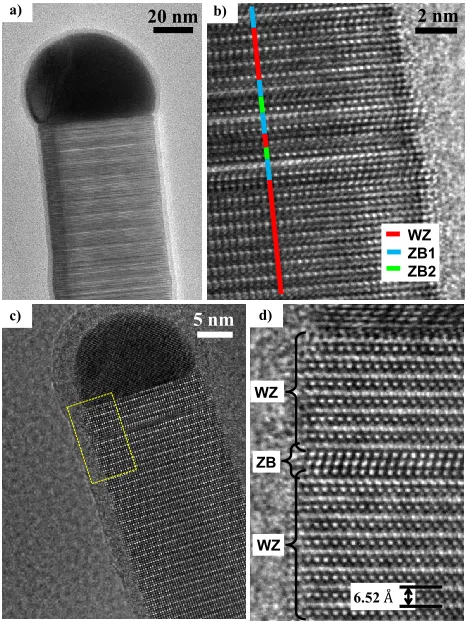
Figure 3(a) shows an image taken near the top of a category 1 wire which has a droplet
diameter of 60 nm. The Au-Ga droplet appears as a dark, truncated ellipsoid at the top of
the wire. A large number of stacking faults appear as bands of lines crossing the growth axis
of the wire. A high-resolution image of a typical region of this wire is shown in 3(b). In this
picture, a coloured line indicates the crystal structure of that portion of the wire, with red
representing WZ structure, and blue and green representing the two possible orientations of
ZB growth when viewed along the 110 direction. The average spacing between stacking
faults is between 1-2nm. The edges of the wire are not perfectly straight, and it is noticed
that wire diameter does not decrease continuously as a function of distance from the foot of
the wire. An example of this can be seen at the bottom of figure 3(a).
Figure 3(c) shows a TEM image taken from a wire from the unpatterned sample having a
20 nm 2 nm
WZ ZB1 ZB2
a) b)
c) 5 nm
6.52 Å WZ
ZB WZ
d)
FIG. 3. (a) TEM image of a category 1 wire with droplet diameter of 60 nm. (b) High resolution
image of typical region from (a). Coloured lines represent the different crystal structures of along
the wire length. (c) TEM image of a category 2 wire with droplet diameter of 17.5 nm. (d) HRTEM
image of area highlighted by yellow rectangle in (c). ‘WZ’ and ‘ZB’ denote wurtzite and zincblende
crystal structure respectively.
droplet appears as a dark hemisphere, and it is clear that the density of stacking faults
is far lower than that seen for the category 1 wire shown in 3(a). A closer view of the
area highlighted by the yellow rectangle in 3(c) is shown in 3(d). Here we can see that a
single atomic layer stacking fault has given rise to a zincblende layer (‘ZB’ in figure 3(d))
while the remainder is wurtzite (‘WZ’ in 3(d)). The average separation of stacking faults
is greater than 8 nm, and the vast majority of stacking faults consisted of single atomic
layer defects as shown in figure 3(d). For the category 1 nanowire, however, the average
separation between defects was 1-2nm, and ZB defects that extended for a number of atomic
layers were common.
As described in the introduction section, WZ crystal structure is expected for VLS growth
[image:7.612.188.422.72.383.2]a) b)
FIG. 4. TEM images showing the contact angle for category 1 (a) and category 2 (b) nanowires.
expected. TEM images of the contact angles of the two wires in figure 3 are shown in figure
4. As can be seen, the contact angle for the category 1 nanowire (which has a droplet
diameter of 60 nm) is approximately 127°, whereas for the category 2 nanowire the value is
only 106°. It appears that the larger contact angle belonging to category 1 wires has given
rise to the high density of ZB defects observed, whereas the contact angle of the category 2
wire, being closer to 90°, has allowed WZ growth with a much lower density of ZB defects.
The bimodal nature of the shapes of the wires expressed in figure 2 is likely to also be related
to the differing contact angle for category 1 and 2 wires. For category 1 wires the diameter
of the droplet is significantly greater than that of the wire. Therefore, it is possible that
during the growth a new GaAs layer will nucleate at a point slightly beyond the width of
the wire itself, resulting in an increase in wire diameter (reverse tapering). This is seen
on occasion in the TEM analysis, as evident towards the bottom of figure 3(a). Hence the
tapering angle of category 1 wires is lower than that of category 2. The difference in height
between the two categories of wires may be related to the fact that there is little variation in
volume from one category to the other (less than 3% difference in average volume of wires
with ϕ= 0−30nm and ϕ= 40−80nm). If volume is constant for both categories of wire
then the height must be greater in category 2 to compensate for the lower tapering angle.
The similarity in volume for both categories of wire suggests that the growth rate is not
sensitive to wire shape, but is governed by the quantity of material incident on the substrate
per unit area.
The origin for the dependency of contact angle on droplet diameter is uncertain. Line
tension, as outlined in the introduction, is one potential cause for this relationship. As
described above, it is known to affect nanodroplets and varies inversely with the radius of
the solid-liquid interface, r. From equation 2, the finding that contact angle is reduced for
It is possible that some cause other than line tension is responsible for the relationship
between droplet diameter and contact angle. It may be the case that the Au:Ga ratio
within the droplet varies slightly as a function of droplet diameter, or that this ratio is
heterogeneous across the sample surface in a manner that depends onϕ. Both of these effects
are known to influence contact angle while not directly linked to line tension27. Another
potential mechanism whereby droplet diameter may influence crystal structure is related to
the location within the droplet at which nucleation of a new layer occurs. It is known that if
nucleation occurs not at the triple-phase line, but at some point of the solid-liquid interface
away from the droplet perimeter, then ZB structure is preferred16. Thus, for larger droplets,
where the solid-liquid interface has a greater surface to perimeter ratio, there may be an
increased likelihood of nucleation away from the triple-phase line resulting in nucleation of
ZB layers. If this is the cause, then rather than the contact angle determining the crystal
structure (as is assumed for the other potential causes), it may be the case that it is the
crystal structure which determines the contact angle, due to the inclination angle of the
{111} wire sidewalls which are associated with ZB growth.
In summary, the size of the catalysing droplet affects the wire shape via a two-step
process. Firstly, the size of the droplet influences the contact angle. Line tension has been
identified as a potential mechanism for this adjustment. If line tension is indeed the cause,
then our finding of larger contact angles for larger droplets indicates a negative value of τ,
which is in agreement with separate studies17,19,22,24. Secondly, the contact angle influences
both the crystal structure and the angle of tapering, the former due to the finding by Glas
et al. that WZ and ZB nucleation energies are contact angle dependent16, and the latter
due to the potential for layers to nucleate beyond the boundary of the underlying layer, as
observed experimentally (bottom of figure 3(a)).
Other potential mechanisms whereby droplet diameter may bring about the findings
observed involve the composition of the AuGa droplet and the potential for nucleation to
occur away from the triple-phase line more readily in larger droplets16,27. In the latter case,
it is possible that the crystal structure determines the contact angle rather than the other
way around.
However, the ability of contact angle to dictate crystal structure seems to be borne out
from an analysis of previous studies. For example, there are a number of investigations where
these are self-catalysed wires), and the structure is found to be predominantly ZB28–33. In
contrast, most studies which find predominantly WZ structure find a contact angle close to
90°(in cases where contact angle was shown or reported)7,12,34,35. In addition, a number of
studies also found a greater density of ZB defects/regions near the foot of nanowires12,16,36,37.
This is likely due to the fact that during the initial stages of nanowire growth the contact
angle is much less than 90°, since the catalysing droplet is situated on a flat surface and the
angle α in equation 2 is therefore equal to zero.
IV. CONCLUSIONS
GaAs nanowires were successfully grown from Au catalyst nanodots which were defined
lithographically. The pattern of the nanowire array broadly reflects that of the grid of Au
nanodots, with a small proportion of deviations due to missing wires and multiple wires per
nanodot site. The positioning of wires in this way allows a thorough statistical analysis.
It was found that the droplet diameter has a critical influence on the resulting shape of
the nanowires, with two distinct categories emerging in terms of height and tapering angle.
These categories were not apparent from a cursory visual inspection of the SEM images.
It is believed that the mechanism by which droplet diameter influences wire shape is via
the dependency of line tension on droplet radius. Line tension determines the contact angle
of the droplet, which in turn affects the crystal structure and wire shape. Aside from line
tension, other mechanisms which may be responsible for the relationship between droplet
size and crystal structure are also explored. An examination of the literature suggests that
there is a strong correspondence between the contact angle and the specific crystal structure,
and yet this relationship is very rarely discussed. These findings highlight the importance
of considering droplet shape when reporting results relating to nanowire growth and when
planning growth conditions, particularly when a specific crystal structure or minimisation
of defects is central to the functionality of proposed devices.
ACKNOWLEDGMENTS
Research in Ireland is supported by the Science Foundation Ireland (SFI) under Contract
Institutions, Cycle 4, National Development Plan 2007-2013 and the Naughton Fellowship
Program. The work at Notre Dame was supported by the National Science Foundation
grant DMR1005851. The research in Poland was partially supported by the European
Union within European Regional Development Fund, through grant Innovative Economy
(POIG.01.01.02-00-008/08).
REFERENCES
1D. P. Burt, N. R. Wilson, J. M. R. Weaver, P. S. Dobson, and J. V. Macpherson, Nano
Letters 5, 639 (2005).
2G. Mariani, A. C. Scofield, C. H. Hung, and D. L. Huffaker, Nature Communications 4,
1497 (2013).
3J. Chen, Y. Y. Dai, J. Luo, Z. L. Li, S. Z. Deng, J. C. She, and N. S. Xu, Applied Physics
Letters 90, 253105 (2007).
4M. S. Gudiksen, L. J. Lauhon, J. Wang, D. C. Smith, and C. M. Lieber, Nature 415, 617
(2002).
5K. A. Dick, Progress in Crystal Growth and Characterization of Materials 54, 138 (2008).
6K. Tivakornsasithorn, R. E. Pimpinella, V. Nguyen, X. Liu, M. Dobrowolska, and J. K.
Furdyna, Journal of Vacuum Science & Technology B: Microelectronics and Nanometer
Structures 30, 02B115 (2012).
7H. Shtrikman, R. Popovitz-Biro, A. Kretinin, L. Houben, M. Heiblum, M. Bukala, M.
Gal-icka, R. Buczko, and P. Kacman, Nano Letters 9, 1506 (2009).
8M. H. Magnusson, K. Deppert, J. O. Malm, J. O. Bovin, and L. Samuelson,
Nanostruc-tured Materials 12, 45 (1999).
9P. Paiano, P. Prete, N. Lovergine, and A. M. Mancini, Journal of Applied Physics 100,
094305 (2006).
10J. C. Harmand, G. Patriarche, N. Pere-Laperne, M.-N. Merat-Combes, L. Travers, and
F. Glas, Applied Physics Letters 87, 203101 (2005).
11M. Plante and R. LaPierre, Journal of Crystal Growth 286, 394 (2006).
12M. Plante and R. LaPierre, Journal of Crystal Growth 310, 356 (2008).
14K. A. Dick, P. Caroff, J. Bolinsson, M. E. Messing, J. Johansson, K. Deppert, L. R.
Wallenberg, and L. Samuelson, Semiconductor Science and Technology25, 024009 (2010).
15J. Johansson, L. S. Karlsson, C. P. T. Svensson, T. Martensson, B. a. Wacaser, K. Deppert,
L. Samuelson, and W. Seifert, Nature Materials 5, 574 (2006).
16F. Glas, J.-C. Harmand, and G. Patriarche, Physical Review Letters 99, 3 (2007).
17H. K. Guo and H. P. Fang, Chinese Physics Letters 22, 787 (2005).
18L. Schimmele and S. Dietrich, The European Physical Journal B 30, 427 (2009).
19J. H. Weijs, A. Marchand, B. Andreotti, D. Lohse, and J. H. Snoeijer, Physics of Fluids
23, 022001 (2011).
20B. Pethica, Journal of Colloid and Interface Science 62, 567 (1977).
21P. Chen, J. Gaydos, and A. W. Neumann, Langmuir 12, 5956 (1996).
22V. Schmidt, S. Senz, and U. G¨osele, Applied Physics A 80, 445 (2004).
23N. Li, T. Tan, and U. G¨osele, Applied Physics A 86, 433 (2007).
24J. Bauer, V. Gottschalch, H. Paetzelt, G. Wagner, B. Fuhrmann, and H. Leipner, Journal
of Crystal Growth 298, 625 (2007).
25V. Pankoke, S. Sakong, and P. Kratzer, Physical Review B 86, 085425 (2012).
26C. Sartel, D. Dheeraj, F. Jabeen, and J. Harmand, Journal of Crystal Growth 312, 2073
(2010).
27A. Amirfazli and A. W. Neumann, Advances in colloid and interface science 110, 121
(2004).
28Y. Heon Kim, D. Woo Park, and S. Jun Lee, Applied Physics Letters 100, 033117 (2012).
29T. Rieger, S. Heiderich, S. Lenk, M. I. Lepsa, and D. Gr¨utzmacher, Journal of Crystal
Growth 353, 39 (2012).
30G. E. Cirlin, V. G. Dubrovskii, Y. B. Samsonenko, A. D. Bouravleuv, K. Durose, Y. Y.
Proskuryakov, B. Mendes, L. Bowen, M. A. Kaliteevski, R. A. Abram, and D. Zeze,
Physical Review B 82, 035302 (2010).
31B. Bauer, A. Rudolph, M. Soda, A. Fontcuberta i Morral, J. Zweck, D. Schuh, and
E. Reiger, Nanotechnology 21, 435601 (2010).
32S. Gibson and R. LaPierre, Physica Status Solidi (RRL) - Rapid Research Letters 7, 845
(2013).
33S. Plissard, K. A. Dick, G. Larrieu, S. Godey, A. Addad, X. Wallart, and P. Caroff,
34D. L. Dheeraj, G. Patriarche, H. Zhou, T. B. Hoang, A. F. Moses, S. Gronsberg, A. T. J.
van Helvoort, B. O. Fimland, and H. Weman, Nano Letters 8, 4459 (2008).
35M. Tchernycheva, J. C. Harmand, G. Patriarche, L. Travers, and G. E. Cirlin,
Nanotech-nology 17, 4025 (2006).
36J. Bauer, H. Paetzelt, V. Gottschalch, and G. Wagner, Physica Status Solidi (B) 247,
1294 (2010).
37F. Glas, G. Patriarche, and J. C. Harmand, Journal of Physics: Conference Series 209,