VMEbus PC/AT
Processor Module
Revision Description Date
A Manual Released 7/94
Trademark Information
Brand or product names are registered trademarks of their respective owners.
Copyright Information
This document is copyrighted by Xycom Incorporated (Xycom) and shall not be reproduced or copied without expressed written authorization from Xycom.
The information contained within this document is subject to change without notice. Xycom does not guarantee the accuracy of the information and makes no commitment toward keeping it up to date.
Address comments concerning this manual to:
CHAPTER TITLE PAGE
1 INTRODUCTION
1.1 Product Features 1-1
1.2 Manual Structure 1-2
1.3 XVME-678/688 Board Operational Description 1-3 1.3.1 80386SX or 486SLC/e Central Processing Unit (CPU) 1-4
1.3.2 DRAM 1-4
1.3.3 Floppy Drive Controller 1-4
1.3.4 Hard Drive Controller 1-4
1.3.5 Graphics Controller 1-5
1.3.6
110
Ports 1-51.3.7 VMEbus Master Interface 1-5
1.3.8 Keyboard Controller 1-5
1.4 Specifications 1-6
2 INSTALLATION
2.1 Introduction 2-1
2.2 Jumpers 2-2
2.2.1 VGA Jumpers (J3, J5) 2-4
2.2.2 EPROM/Flash Jumper (J1) 2-4
2.2.3 IRQ12 Jumper (J8) 2-4
2.2.4 Battery and Test Jumpers (J2, J4) 2-5
2.3 Switch Settings 2-5
2.4 Connectors 2-6
2.4.1 VMEbus PI Connector 2-8
2.4.2 VMEbus P2 Connector 2-9
2.4.3 Floppy Drive Connector (P4) 2-10
2.4.4 IDE Hard Drive Connector (P5) 2-11
2.4.5 Keyboard Connector (P6) 2-12
2.4.6 Auxiliary Connector (P7) 2-12
2.4.7 COM2 Serial Port Connector (P8) 2-12
2.4.8 COM 1 Serial Port Connector (P9) 2-13
2.4.9 VGA Connector (PlO) 2-13
2.4.10 Parallel Port Connector (JKl) 2-14
2.4.11 Speaker Connector (17) 2-14
2.4.12 PXTI Connector 2-15
2.4.13 PATI Connector 2-16
Table of Contents
CHAPTER TITLE PAGE
3 BIOS SETUP MENUS
3.1 Introduction 3-1
3.2 Software Control and Initial Setup 3-1
3.3 BIOS Main Menu 3-2
3.3.1 BIOS Setup Menu 3-3
3.3.2 VMEbus Master Setup Menu 3-8
3.3.3 Solid State Disk Setup Menu 3-11
3.3.4 Extended BIOS Features Menu 3-13
3.3.5 System Information Menu 3-16
3.3.6 Diagnostics Menu 3-16
3.3.7 Format Fixed Disk Menu 3-23
4 PROGRAMMING
4.1 Introduction 4-1
4.2 XVME-678/688 Memory Maps 4-1
4.2.1 DRAM 4-7
4.2.2 EPROM 4-8
4.3 Accessing VMEbus Memory Space Using the
Real Mode Window 4-9
4.3.1 EPROM 4-9
4.3.2 VMEbus lACK Space 4-9
4.3.3 VMEbus Short 110 Space 4-10
4.3.4 VMEbus Standard Address Space 4-11
4.4 VMEbus Master Interface 4-12
4.5 Shadow RAM Option 4-14
4.6 110 Port Addresses 4-15
4.6.1 Control Register 1 4-17
4.6.2 Auxiliary Interrupt 4-18
4.6.3 Status Register 1 4-18
4.6.4 Status Register 2 4-19
4.6.5 VMEbus HI Address 4-19
4.6.6 Control Register 2 4-19
4.6.7 Control Register 3 4-20
4.6.8 Control Register 4 4-20
4.6.9 Control Register 5 4-21
4.6.10 Control Register 6 4-21
4.7 Interrupts 4-22
4.7.1 Auxiliary Maskable Interrupts (AMIs) 4-22
CHAPTER 4
5
4.8.3 4.94.10
5.1
5.2
5.2.1
5.2.2
5.2.3
5.2.4
5.2.5
5.2.6
5.3
5.3.1
5.3.2
5.4
5.4.1
5.4.2
5.4.3
5.4.4
5.4.5
5.4.6
5.5
5.5.1
5.5.2
5.5.3
5.5.4
5.5.5
5.5.6
5.6
5.6.1
5.6.2
5.6.3
5.6.4
5.6.5
5.6.6
TITLEPROGRAMMING (continued)
Numeric Consistency System Resource Function CMOS RAM
XVME BIOS FUNCTIONS
XVME BIOS Functions Miscelleneous Functions Identify XVME Model
Get Real Mode Window Physical Segment Get LED Configuration
Set LED Configuration
Get Flash BIOS Write Configuration Set Flash BIOS Write Configuration Real Mode Window (RMW) Functions Get Real Mode Window Configuration Set Real Mode Window Configuration
PAGE 4-28 4-30 4-31
5-1
5-4
5-4
5-5
5-6
5-7 5-8 5-9Auxiliary Non-maskable Interrupt (ANMI) Functions Get ANMI Group Configuration
5-10
5-10
5-115-12
5-12
5-135-14
5-15
5-16
5-17 5-18 5-18 5-195-21
5-22
5-23
5-24
5-25
5-25
5-26
5-27 5-285-30
5-32
Set ANMI Group Configuration Get ANMI Mask
Set ANMI Mask Get ANMI Status Clear ANMI
VMEbus Master Functions
Get VMEbus Master Configuration Set VMEbus Master Configuration Get VMEbus Ownership Configuration Set VMEbus Ownership Configuration Get VMEbus Ownership Status
Wait for VMEbus Ownership to be Granted VMEbus Interrupt Handler Functions Get VMEbus Interrupt Group Configuration Set VMEbus Interrupt Group Configuration Get VMEbus Interrupt Mask
Set VMEbus Interrupt Mask
Table of Contents CHAPTER 5 A B C D 5.6.7 5.6.8 5.7 5.7.1 FIGURE 1-1 2-1 2-2 2-3 2-4 2-5 3-1 3-2 3-3 3-4 3-5 3-6 3-7 3-8 3-9 3-10 3-11 3-12 3-13
TITLE PAGE
XVME BIOS FUNCTIONS (continued)
Determine Highest Priority Pending VMEbus Interrupt 5-33 Acknowledge VMEbus Interrupt Via Real Mode Window 5-34 VMEbus System Resource Functions 5-35
Get System Resource Flag 5-35
APPENDICES
VMEbus CONNECTOR/PIN DESCRIPTIONS QUICK REFERENCE GUIDE
EXTENDED VGA MODES
BLOCK DIAGRAM, ASSEMBLY DRAWING, AND SCHEMATICS
LIST OF FIGURES
TITLE PAGE
XVME-678/688 Board Block Diagram 1-3
XVME-678/688 Jumper and Switch Locations 2-3
XVME-678/688 Connector Locations 2-7
XVME-678/688 Board Front Panel 2-19
DRAM Installation 2-24
80387SX Math Co-processor Installation 2-25
Main Setup Menu 3-2
BIOS Setup Menu 3-3
VMEbus Master Setup Menu 3-8
Solid State Disk Setup Menu 3-11
Extended BIOS Features Menu 3-13
System Information Menu 3-16
Advanced Diagnostics Menu 3-17
Advanced Diagnostics Test Menu 3-18
Diskette Drive Menu 3-20
Fixed Disk Menu 3-21
Parallel Port Test Menu 3-22
Serial and Parallel Loopback Connections 3-22
FIGURE 4-2 4-3 4-4 4-5 4-6 4-7 4-9 4-10 4-11 4-12 4-13 4-14 TABLE 1-1 2-1 2-2 2-3 2-4 2-5 2-6 2-7 2-8 2-9 2-10 2-11 2-12 2-13 2-14 2-15 2-16 3-1
LIST OF FIGURES (continued)
TITLE PAGE
2 Mbyte Memory Map (as seen by the CPU) 4-3 4 Mbyte Memory Map (as seen by the CPU) 4-4 10 Mbyte Memory Map (as seen by the CPU) 4-5 16 Mbyte Memory Map (as seen by the CPU) 4-6
EPROM Memory Map 4-8
BERR Mapped Onto IOCHCK* 4-12
BERR, SYSFAIL, and ABORT Switch Mapped on IRQI04-24 Auxiliary Non-maskable Interrupt Structure 4-25
Byte-Ordering Schemes· 4-26
Maintaining Address Consistency 4-27
Maintaining Numeric Consistency 4-28
Reset Structure 4-30
LIST OF TABLES
TITLE PAGE
XVME-678/688 Module Specifications 1-6
XVME-678/688 Jumper Options 2-4
XVME-678/688 SWI Switch Settings 2-5
PI Pinouts 2-8
P2 Pinouts 2-9
Floppy Drive Connector 2-10
IDE Hard Drive Connector 2-11
Keyboard Connector 2-12
Auxiliary Connector 2-12
COM2 Serial Port Connector 2-12
COM1 Serial Port Connector 2-13
VGA Connector 2-13
Parallel Port Connector 2-14
Speaker Connector 2-14
PXT 1 Pinouts 2-15
PAT 1 Pinouts 2-16
Bank and SIMM Size 2-22
1.1 PRODUCT FEATURES
The XVME-678/688 VMEbus PCI A T processor modules are designed to combine the high-performance and ruggedized packaging of the VMEbus with the broad application software base of the IBM PCI AT standard. These 6U, double-high modules require a single VMEbus slot, are fully AT -compatible, and support all standard PCI AT software.
The XVME-688 features a low-power CMOS design with an 80386SX processor running at 25 MHz. The XVME-678 features a Cyrix 486SLC/e running at 25 MHz. The 486SLC/e provides an internal 1 Kbyte cache, a 486SX-compatible instruction set, and a 80386SX pin out.
Both modules offer the following features:
• 25 MHz 80386SX microprocessor (XVME-688) or 25 MHz 486SLC/e (XVME-678) • 0, 1, or 4 Mbytes of DRAM
-SIMM sockets for memory expansion up to 16 Mbytes DRAM
-Zero wait state page interleaved DRAM accesses with 60 nsec DRAMs • Shadow RAM option for System and VGA BIOS
• Super VGA graphics controller with 512 Kbytes of DRAM • Floppy disk controller
• High-performance IDE hard disk controller • A socket for an 80387SX math co-processor • VMEbus master interface
• VMEbus interrupt handler • Programmable interrupt enable
• Programmable bus request and bus grant levels • VMEbus slot 1 functions
• Real mode window, allowing VMEbus Short I/O and Standard address space locations to be accessed while processor is in real mode
• Two RS-232C serial communication ports • Centronics-compatible parallel port • PS/2-compatible keyboard port
Chapter 1 -Introduction
1.2 MANUAL STRUCTURE
The chapters in this manual are organized in the following manner:
Chapter One Module Description: functional and environmental specifications, module structure, VMEbus compliance information, and blo.ck diagram
Chapter Two Installation: system requirements, jumper and switch settings, connector pinouts, and procedures for installing the XVME-678/688 into a backplane, installing SIMM memory onto the XVME-678/688, adding extended BIOS. and installing the optional math co-processor
Chapter Three BIOS Setup Menus: descriptions of menu-driven BIOS utilities
Chapter Four Programming: information required to program the module, including memory maps, I/O maps, and interrupt information
Appendix A VMEbus Connector/Pin Description: VMEbus signals, connectors, pin numbers and their descriptions
Appendix B Quick Reference Guide: default jumper settings, tables, and graphs
Appendix C Extended VGA Modes: information about extended video modes
1.3 XVME-678/688 BOARD OPERATIONAL DESCRIPTION
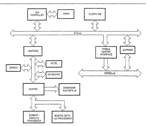
Figure 1-1 shows the logical arrangement of the XVME-678/688 board.
VGA CONTROLLER
BUFFERS
SCATSX
DRAM
ATbus
DRAMSIMM SOCKETS (4)
t..-c ---'{
--~----,
80386SXI 486SLC/e PROCESSOR
80387SX MATH CO-PROCESSOR
FLOPPY IDE
VMEbus
[image:13.617.66.544.208.620.2]Chapter 1 - Introduction
1.3.1 80386SX or 486SLC/e Central Processing Unit (CPU)
The XVME-688 uses an 80386SX microprocessor to provide operational capabilities. The XVME-678 uses a Cyrix 486SLC/e that provides a 486SX-compatible instruction set with a 1 Kbyte internal cache. These 25 MHz CPUs can access up to 16 Mbytes of DRAM.
1.3.2 ])1lAJ\I
The XVME-678/688 uses Dynamic Random Access Memory (DRAM) configured in a page interleave mode with 0 wait-state operation. The 1, 4, and 16 Mbyte versions of the XVME-678/688 are two-way interleaved, while the 2 and 10 Mbyte versions have no interleaving.
The XVME-678/688 comes factory-configured with 0, 1, or 4 Mbytes of DRAM. Additional DRAM can be installed in 2, 10, and 16 Mbyte configurations. Refer to section 2.7 for more information.
1.3.3 Floppy])rive Controller
The XVME-678/688 floppy drive controller can support up to two PC/AT-compatible floppy drives. These drives can be any combination of 360 Kbytes, 720 Kbytes, 1.2 Mbytes, and 1.44 Mbytes.
1.3.4 Hard ])rive Controller
The XVME-678/688 uses the IDE interface for the hard drive controller. This 16-bit interface provides complete hardware-level compatibility to the IBM PC/AT hard drive controller. Two drives can be connected to the interface by daisy chaining the ribbon cable and setting one drive as the master and one as the slave. (This requires setting jumpers on the drive. Consult your drive manual for more information. )
CAUTION
The IDE ribbon cable should not exceed 18 inches. Otherwise, errors may occur and data may be corrupted.
1.3.5 Graphics Controller
The XVME-678/688 VGA graphics controller supports all IBM VGA, EGA, CGA, and MDA modes to the register level. The VGA adapter supports Super VGA up to 1024 x 768 with 16 colors. The VGA BIOS is 8 bits. Shadowing the BIOS through the BIOS Setup Menu (see Chapter 3 for more information) significantly increases system performance.
The VGA controller supports IBM modes 0-13H (hex) as well as other modes. See Appendix C for a complete list of supported modes.
1.3.6 I/O Ports
The XVME-678/688 has two RS-232C serial ports and one IBM PC/AT style Centronics-compatible parallel port. These ports are controlled in the BIOS Setup Menu which allows the ports to be disabled or enabled from software. Interrupts are enabled or disabled by setting bits in 110 registers (refer to Chapter 5).
1.3.7 VMEbus Master Interface
The VMEbus master interface allows the 80386SX CPU to become a master or interrupt handler on the VMEbus. The XVME-678/688 master interface is invoked whenever the 80386SX accesses the VMEbus Standard, Short 110, or lACK address spaces. All accesses to the VMEbus are through the Real Mode Window.
1. 3.8 Keyboard Controller
Chapter 1 - Introduction
1.4 SPECIFICATIONS
Table 1-1 contains the functional specifications for the XVME-678/688.
Table 1-1. XVME-678/688 Module Specifications
SPECIFICATION
Mechanical
Processor XVME-688 XVME-678
Processor Speed
AT-bus Speed
Math Co-processor (optional)
Graphics Controller
Floppy Disk Interface
Hard Disk Interface
PS/2 A UX Port
Serial Ports (2)
Parallel Port
Power Requirements
+5 V @ 1.9 A typ., 2.7 A max.
SIMM Memory Configuration SIMM Sites
Memory Configurations Memory Accepted Memory Speed Required
DESCRIPTION
80386SX· 486SLC/e
25 MHz
10 or 8.33 MHz
80387SX
VGA analog output
Max. resolution: 1024 x 768, 16 colors
PC/AT-compatible: supports two
drives-360 Kbyte, 720 Kbyte, 1.2 Mbyte, and 1.44 Mbyte capacities
IDE controller: supports two drives
Compatible with PS/2 mouse
RS-232C
Centronics compatible
+ 12 V @ 2 rnA max.
-12 V @ 1 rnA max.
4
Table 1-1. XVME-678/688 Module Specifications (continued)
SPECIFICATION
Environmental
Temperature Operating Non-operating
Humidity
Altitude Operating Non-operating
Vibration Operating
Non-operating
Shock
Operating
Non-operating
VMEbus
DESCRIPTION
0° to 65° C (32° to 149°F) -40° to 85°C (-40° to 185°F)
5 to 95 % RH, non-condensing
Sea level to 10,000 ft. (3048 m) Sea level to 50,000 ft. (15240 m)
5 to 2000 Hz
.015" peak to peak displacement 2.5 g max acceleration
.030" peak to peak displacement 5.0 g max acceleration
30 g peak acceleration, 11 msec duration 50 g peak acceleration, 11 msec duration
Complies with VMEbus Specification IEEE 1014 A24/AI6:DI6/D08(EO) Master
R(0-3) Bus Requester
Interrupt Handler IH(I)-IH(7) SYSCLK and SYSRESET Driver SGL Arbiter
ROR Option
2.1 INTRODUCTION
This chapter provides the information necessary to configure the XVME-678/688 VMEbus PC/AT Processor Module. It also provides information on installing the XVME-678/688 into a backplane, adding extended BIOS to the XVME-678/688, adding DRAM memory in SIMM sockets, and installing an optional math co-processor.
WARNING
If the battery is disabled in your system, please do the following: Upon enabling, your module must be powered up for a minimum of 30 seconds. Failure to follow this procedure may result in premature battery failure.
WARNING
XVME-678/688 CPU modules with functional revision levels of 4.1 or higher (functional revision levels and part numbers are located on a label on the PI connector) feature a 16-bit compatible PC/104 expansion site. This PC/104 expansion site requires a new version of the XVME-956 Modular I/O Carrier Module. If the CPU module's functional revision level is 4.1 or higher, use the XVME-956/12 (part number 70956-012). If the functional revision level is less than 4.1, use the XVME-956/2 (part number 70956-002). Do not use the XVME-956/2 on a CPU module with functional revision levels of 4.1 or higher as this may cause damage to both modules.
In addition, the XVME-956/402 SCSI Expansion Module has been updated. The XVME-956/412 must be used with XVME-678/688 modules that have a functional revision level of 4.1 or higher. Use of the XVME-956/402 with the new CPU modules will damage the SCSI Expansion Module and the CPU.
Chapter 2 - Installation
NOTE
The XVME-678/688 module obtains power from both the VMEbus PI and P2 backplanes. However, only PI is necessary for proper operation.
2.2 JUMPERS
All of the jumpers on the XVME-678/688 are shipped in the correct positions. The unit will function as required with no modifications.
NOTE
Jumpers
only
need to be modified when disabling VGA or replacing the BIOS EPROM with Flash RAM devices.~J3
SA
~J2 SA
[image:21.613.64.557.218.584.2]Chapter 2 - Installation
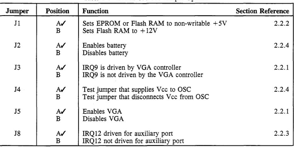
Table 2-1. XVME-678/688 Jumper Options
Jwnper Position Function Section Reference
11 A.t Sets EPROM or Flash RAM to non-writable + 5V 2.2.2 B Sets Flash RAM to + 12V
12 A.t Enables battery 2.2.4
B Disables battery
13 A.t IRQ9 is driven by VGA controller 2.2.1
B IRQ9 is not driven by the VGA controller
J4 A.t Test jumper that supplies V cc to OSC 2.2.4
B Test jumper that disconnects V cc from OSC
J5 A.t Enables VGA 2.2.1
B Disables VGA
J8 A.t IRQ12 driven for auxiliary port 2.2.3
B IRQ12 not driven for auxiliary port
.t indicates default settings
2.2.1 VGA Jwnpers (J3, J5)
Jumper J5 enables the VGA BIOS and Xycom Setup when positioned to A (default) or disables the VGA BIOS and XYCOM Setup when positioned to B.
Jumper 13 should be set to A (default) for IRQ9 to be driven by the VGA, or to B for IRQ9 not to be driven by the VGA.
2.2.2 EPROM/Flash Jwnper (Jl)
Jumper 11 sets EPROM and Flash RAM devices to a non-writable +5V when positioned to A (default). When positioned to B, 11 sets Flash RAM devices to + 12V.
2.2.3 IRQ12 Jwnper (J8)
2.2.4 Battery and Test Jwnpers (J2, J4)
Jumper J2 enables the XVME-678/688 on-board battery when positioned to A (default), and disables the battery when positioned to B. This jumper should remain positioned to A. To disable the battery, position switch 6 of SWI to open (see Section 2.3). See WARNING in Section 2.1 regarding a disabled battery.
Jumper J4 is a test jumper that supplies Vcc to OSC. This jumper must always remain positioned to A.
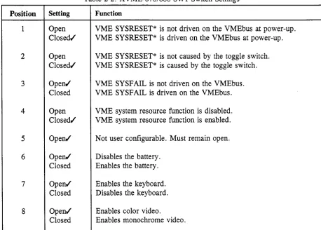
2.3 SWITCH SETTINGS
The XVME-678/688 has one eight-position switch, SWI. This switch allows critical options, which are not software accessible, to be enabled in a common area. Figure 2-1 on page 2-2 shows the switch location. The settings and their functions are shown in the table below.
Table 2-2. XVME-678/688 SWI Switch Settings
Position Setting Function
1 Open VME SYSRESET* is not driven on the VMEbus at power-up. Closedvi' VME SYSRESET* is driven on the VMEbus at power-up.
2 Open VME SYSRESET* is not caused by the toggle switch. Closedvi' VME SYSRESET* is caused by the toggle switch.
3 Openvi' VME SYSFAIL is not driven on the VMEbus. Closed VME SYSFAIL is driven on the VMEbus.
4 Open VME system resource function is disabled. Closedvi' VME system resource function is enabled.
5 Openvi' Not user configurable. Must remain open.
6 Openvi' Disables the battery. Closed Enables the battery.
7 Openvi' Enables the keyboard. Closed Disables the keyboard.
8 Openvi' Enables color video.
[image:23.612.71.529.321.649.2]Chapter 2 - Installation
NOTE
The battery enable switch (SW6) is shipped in the OPEN position. Close this switch to allow the CMOS configuration to be retained on power-down.
2.4 CONNECTORS
The XVME-678/688 has 12 connectors:
• IDE hard drive • Floppy drive • Parallel port
• COM1 and COM2 serial ports • PS/2 A UX port
• VGA • Keyboard • Speaker
• VMEbus P 1 and P2
• PC/l 04-compatible expansion site
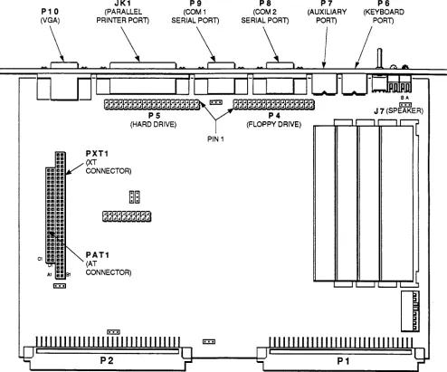
The connectors must be clean, dry, and undamaged at the time of installation. Figure 2-2 on the following page shows the location of the connectors on the board.
NOTE
P10 (VGA) 1111 1111 1111 1111 1111 1111 1111 1111 1111 1111 1111 1111 1111 1111 1111 1111 1111 1111 1111 1111 1111 1111 1111 1111 1111 1111 1111 1111 1111 1111 1111 1111 1111 1111 1111 1111 1111 II C1 tE:::E::l JK1 (PARALLEL PRINTER PORT) PXT1 (XT CONNECTOR)
mm
PAT1 (AT CONNECTOR) tE:::E::l P9 (COM 1 SERIAL PORT)PIN 1
tE:::E::l P8 (COM 2 SERIAL PORT) P7 (AUXILIARY PORT) P6 (KEYBOARD PORT) SA tE:::E::l J 7 (SPEAKER)
r--l r--l r--l r-;:J
[image:25.612.59.553.189.600.2]Chapter 2 - Installation
2.4.1 VMEbus PI Connector
VMEbus PI is a 96-pin DIN connector.
Table 2-3. PI Pinouts
Pin Row A Signal Row B Signal Row C Signal
1 DO BBUSY D08
2 DOl BCLR* D09
3 D02 ACFAIL* D10
4 D03 BGOIN* Dll
5 D04 BGOOUT* D12
6 D05 BGlIN* D13
7 D06 BG10UT* D14
8 D07 BG2IN* D15
9 GND BG20UT* GND
10 SYSCLK BG3IN* SYSFAIL*
11 GND BG30UT* BERR*
12 DS1* BRO* SYSRESET*
13 DSO* BRl* LWORD*
14 WRITE * BR2* AM5
15 GND BR3* A23
16 DTACK* AMO A22
17 GND AMI A21
18 AS* AM2 A20
19 GND AM3 A19
20 IACK* GND A18
21 IACKIN* SERCLK A17
22 IACKOUT* SERDAT* A16
23 AM4 GND A15
24 A07 IRQ7* A14
25 A06 IRQ6* A13
26 A05 IRQ5* A12
27 A04 IRQ4* All
28 A03 IRQ3* A10
29 A02 IRQ2* A09
30 AOI IRQ1* A08
31 -12V +5V STDBY +12V
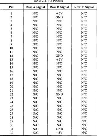
2.4.2 VMEbus P2 Connector
[image:27.613.141.469.162.622.2]VMEbus P2 is a 96-pin DIN connector.
Table 2-4. P2 Pinouts
Pin Row A Signal Row B Signal
1
N/C
+5V2
N/C
GND3
N/C
N/C
4
N/C
N/C
5
N/C
N/C
6
N/C
N/C
7
N/C
N/C
8
N/C
N/C
9
N/C
N/C
10
N/C
N/C
11
N/C
N/C
12
N/C
GND13
N/C
+5V14
N/C
N/C
15
N/C
N/C
16
N/C
N/C
17
N/C
N/C
18
N/C
N/C
19
N/C
N/C
20
N/C
N/C
21
N/C
N/C
22
N/C
GND23
N/C
N/C
24
N/C
N/C
25
N/C
N/C
26
N/C
N/C
27
N/C
N/C
28
N/C
N/C
29
N/C
N/C
30
N/C
N/C
31
N/C
GND32
N/C
+5VRow C Signal
Chapter 2 - Installation
2.4.3 Floppy Drive Connector (P4)
The floppy drive connector is a 34-pin header located on the board near P8, the COM2 serial port connector. It is the interface and control connection for up to two floppy drives.
Table 2-5. Floppy Drive Connector
Pin Signal Pin Signal
1 GND 18 FDIRC*
2 FRWC* 19 GND
3 GND 20 FSTEP*
4 N/C 21 GND
5 KEY 22 FWD*
6 N/C 23 GND
7 GND 24 FWE*
8 IDX* 25 GND
9 GND 26 FTKO*
10 Mal 27 GND
11 GND 28 FWP*
12 FDS2 29 GND
13 GND 30 FRDD*
14 FDS1 31 GND
15 GND 32 FHS*
16 M02 33 GND
2.4.4 IDE Hard Drive Connector (P5)
The IDE hard drive connector is a 40-pin header located near JK1, the parallel port. It is the control connector for any hard drive(s) interfaced with the XVME-678/688. The XVME-678/688 can control up to two hard drives from this connector.
Table 2-6. IDE Hard Drive Connector
Pin Signal Pin Signal
1 RESET* 21 N/C
2 GND 22 GND
3 ID87 23 IOW*
4 SD8 24 GND
5 SD6 25 IOR*
6 SD9 26 GND
7 SD5 27 N/C
8 SDlO 28 ALE
9 SD4 29 N/C
10 SD11 30 GND
11 SD3 31 ATIRQ14
12 SD12 32 ATIOCS16*
13 SD2 33 SAl
14 SD13 34 N/C
15 SD1 35 SAO
16 SD14 36 SA2
17 SDO 37 HCSO
18 SD15 38 HCS1
19 GND 39 N/C
Chapter 2 - Installation
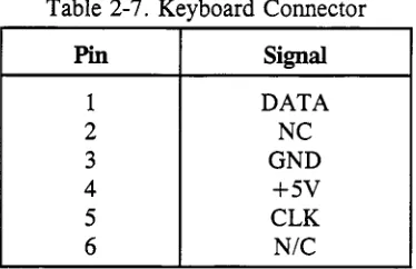
2.4.5 Keyboard Connector (P6)
P6, a 6-pin MINI DIN connector, serves as the interface point for a keyboard. An interface cable is shipped with the XVME-678/688 so a standard PC/AT keyboard can be used.
Table 2-7. Keyboard Connector
Pin Signal
1 DATA
2 NC
3 GND
4 +5V
5 CLK
6 N/C
2.4.6 Auxiliary Connector (P7)
P7 is a PS/2-compatible, 6-pin MINI DIN connector. This port accepts a PS/2-compatible mouse, track ball, etc.
Table 2-8. Auxiliary Connector
Pin Signal
1 DATA
2 NC
3 GND
4 +5V
5 CLK
6 N/C
2.4.7 COM2 Serial Port Connector (P8)
The 9-pin D subminiature COM2 serial port connector is located on the module's front panel.
Table 2-9. COM2 Serial Port Connector
Pin Signal Pin Signal
1 DCD2 6 DSR2
2 RXD2 7 RTS2
3 TXD2 8 CTS2
[image:30.612.211.398.175.296.2] [image:30.612.209.397.386.508.2]2.4.8 COMl Serial Port Connector (P9)
The 9-pin D subminiature COMI serial port connector, P9, is located on the module's front panel.
Table 2-10. COMI Serial Port Connector
Pin Signal Pin Signal
1 DCDI 6 DSRI
2 RXDI 7 RTSI
3 TXDI 8 CTSI
4 DTRI 9 RII
5 GND
2.4.9 VGA Connector (PlO)
The VGA connector, P1O, is a 15-pin subminiature located at the bottom of the module's front panel.
Table 2-11. VGA Connector
Pin Signal Pin Signal
1 RED 9 KEY
2 GREEN 10 GND
3 BLUE 11
N/C
4
N/C
12N/C
5 GND 13 HSYNC
6 GND 14 VSYNC
7 GND 15
N/C
Chapter 2 -Installation
,
2.4.10 Parallel Port Connector (JKl)
JK1 is a 25-pin female D subminiature connector located on the module's front panel.
Table 2-12. Parallel Port Connector
Pin Signal Pin Signal
1 STROBE 14 AUTOFEED
2 PDOUTO 15 PERROR
3 PDOUTI 16 INIT
4 PDOUT2 17 SELIN
5 PDOUT3 18 GND
6 PDOUT4 19 GND
7 PDOUT5 20 GND
8 PDOUT6 21 GND
9 PDOUT7 22 GND
10 PACK 23 GND
11 PBUSY 24 GND
12 PE 25 GND
13 SELECT
2.4.11 Speaker Connector (J7)
17 is a three-pin header located on the board near the LEDs.
Table 2-13. Speaker Connector
Pin Signal
1 SIGNAL
2 +5V
[image:32.613.212.401.449.534.2]2.4.12 PXTl Connector
The PC/104-compatible PXT1 is a two-row, 64-pin connector. It allows a single card expansion to XVME-678/688 without an adapter card. This interface incorporates the power that allows plug-in adapters to be free of the need for a PI or P2 connection.
Table 2-14. PXTl Pinouts
Pin Row A Signal Row B Signal
1 IOCHCHK* GND
2 SD7 RESETDRV
3 SD6 +5V
4 SD5 IRQ9
5 SD4
N/C
6 SD3 DRQ2
7 SD2 -12V
8 SD1
N/C
9 SDO +12V
10 IOCHRDY KEY
11 AEN SMEMW*
12 SA19 SMEMR*
13 SA18 IOW*
14 SA17 IOR*
15 SA16 DACK3*
16 SA15 DRQ3
17 SA14 DACK1*
18 SA13 DRQ1
19 SA12 REF*
20 SAll SYSCLK
21 SAlO IRQ7
22 SA9 IRQ6
23 SA8 IRQ5
24 SA7 IRQ4
25 SA6 IRQ3
26 SA5 DACK2*
27 SA4
TIC
28 SA3 ALE
29 SA2 +5V
30 SAl OSC
31 SAO GND
Chapter 2 - Installation
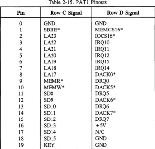
2.4.13 PATl Connector
[image:34.613.145.461.184.487.2]PAT1 is a two-row, 40-pin connector that allows a single card expansion to XVME-678/688 without an adapter card. This interface incorporates the power that allows plug-in adapters to be free of the need for a PI or P2 connection.
Table 2-15. PAT1 Pinouts
Pin Row C Signal Row D Signal
0 GNO GNO
1 SBHE* MEMCS16*
2 LA23 IOCS16*
3 LA22 IRQ 10
4 LA21 IRQ11
5 LA20 IRQ12
6 LA19 IRQ15
7 LA18 IRQ 14
8 LA17 OACKO*
9 MEMR* ORQO
10 MEMW* DACK5*
11 S08 ORQ5
12 S09 OACK6*
13 SOlO ORQ6
14 SOlI OACK7*
15 S012 ORQ7
16 S013 +5V
17 S014 N/C
18 S015 GNO
2.5 INSTALLING THE XVME-678/688 INTO A BACKPLANE
This section provides the information necessary to install the XVME-678/688 PCI AT Processor Module into the VMEbus backplane.
Xycom modules are designed to comply with all physical and electrical VMEbus backplane specifications. The XVME-678/688 is a double-high, single-board VMEbus module. As such, it requires one slot with either just the PI VMEbus backplane, or with both the PI and P2 backplanes.
The XVME-955 Hard Disk/Floppy Disk Module, available from Xycom, is ideally suited for use with the XVME-678/688. It combines a high-capacity 3.5" IDE drive and a 3.5" 1.44 Mbyte micro-floppy into a unit that occupies only two double-high VMEbus slots. Ask your Xycom representative for details.
WARNING
Do not install or remove any boards before turning off the power to the bus and all related external power supplies.
1. Disconnect all power supplies to the backplane and/or terminal.
2. Make sure the backplane PI and P2 connectors are accessible.
3. Verify all jumper settings.
4. If using the Intel80387SX math co-processor, install it in socket U7 of the XVME-678/688. Refer to Section 2.8 for more detailed diagrams.
5. Position SWI switch 6 to closed to enable the on-board battery.
6. Connect the floppy disk cable to P4 on the component side of the XVME-678/688 board. Refer to Figure 2-2 on page 2-6 for the location of P4.
7. Connect the IDE hard drive cable to P5 on the component side of the XVME-678/688 module. Refer to Figure 2-2 on page 2-6 for the location of P5.
Chapter 2 - Installation
9. Make sure the cardcage slot that will hold the XVME-678/688 is clear and accessible. If using the XVME-678/688 in conjunction with the XVME-955 module, make sure that the two cardcage slots to the right of the XVME-678/688 (which will hold the XVME-955) are also clear.
10. Install the XVME-678/688 into the cardcage by centering the unit on the plastic guides in the slots (PI connector facing up) and pushing the boards slowly toward the rear of the chassis until the PI and P2 connectors engage. The boards should slide freely in the plastic guides.
CAUTION
Do not use excessive force or pressure to engage the connectors. If the boards do not properly connect with the backplane, remove the module and inspect all connectors and guide slots for possible damage or obstructions.
11. Secure the module to the chassis by tightening the machine screw at the top and bottom of each board.
12. Connect all remaining peripherals by attaching each interface cable into the appropriate connector on the front of the XVME-678/688 board as follows: VGA cable-VGA, keyboard-KEYBD, serial devices-COM 1 and COM2, and parallel device-LPTl. Refer to Figure 2-2 on page 2-6 for locations of these connectors.
XVME·688
(I FAIL
C)PASS ABORT
(!) RESET KEYBD
(;)
AUOX••• •• •
.
•
xycom
Chapter 2 - Installation
2.6 ADDING EXTENDED BIOS
The XVME-678/688 has one 256Kx8 EPROM that can represent the entire IBM BIOS range. The device address is the physical address which is viewed from an EPROM programmer such as a Data I/O. The system address is the address the code appears at when plugged into the EPROM site on the XVME-678/688, as addressed by the 80386SX processor.
A diagram of the XVME-678/688 and EPROM programmer addresses is shown below:
Device Address
30000-3FFFFF
20000-2FFFF
10000-1 FFFF
08000-0FFFF
00000-07FFF
System BIOS
64K
Diagnostics
64K
User Area
64K
User Area
32K
Video BIOS
32K
System Address
FOOOO-FFFFF
EOOOO-OEFFFF
DOOOO-DFFFF
CBOOO-CFFFF
COOOO-C7FFF
Adding on-board extended BIOS to the XVME-678/688 involves two major steps: programming the EPROM and setting the Extended BIOS Setup Menu.
Programming the EPROM
Before beginning, make sure your EPROM programmer supports 2-Mbit devices.
1. Remove the 32-pin EPROM from socket U8.
2. Place the EPROM into the EPROM programmer's socket.
3. Load the EPROM into the RAM of the programmer. Set the starting address at OH.
NOTE
At this point, the data should be stored to a disk to protect the information in case of an error in programming.
5. Use a UV light to erase the EPROM.
6. Place your extended EPROM programmer RAM starting at location lOOOOH. The code should not exceed 64 Kbytes.
7. Reburn the EPROM with the new code. This places the new extended BIOS in the DOOO:OOOO-DOOO:FFFF block.
NOTE
At this point, the data should be stored to a disk to protect the information in case of an error in programming.
8. Place the EPROM back into socket U8 on the XVME-678/688.
Setting
theEPROM
Menu1. Power-up the XVME-678/688. After the memory tests, press
<
Ctrl ><
Alt ><
S > simultaneously to enter the Extended BIOS Menu.2. Use the arrow keys to highlight Solid State Disk Setup and press
<
Enter> to select this menu.3. Enable the on-board extended BIOS from DOOOO-DFFFF and disable the BIOS from EOOOO-EFFFF.
4. Select FlO to save the configuration, and then press
<
Esc> to exit the menu.Chapter 2 - Installation
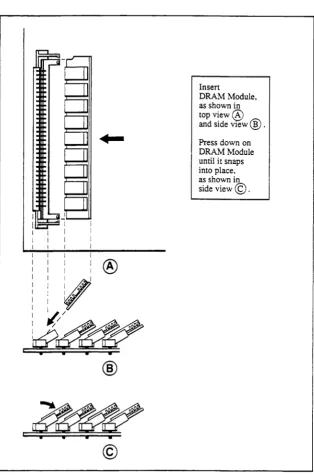
2.7 INSTALLING DRAM
The XVME-678/688 has four SIMM sites in which to add memory. Due to the 25 MHz CPU speed, the access time of the DRAM interface is very important. To run at 0 wait states, the SIMMs must have the following access times:
• 60 ns access time for nine chip DRAM SIMMs • 70 ns access time for three chip DRAM SIMMs
If you opt for 80 ns DRAMs, change the 0 wait state option to 1, wait state in the Setup Menu.
NOTE
Three-chip memory modules are recommended to meet the VME height specifications.
The XVME-678/688 can accommodate 1, 2, 4, 10 or 16 Mbytes of DRAM, mounted on SIMM strips. SIMM strips with 256Kx9, 1Mx9, or 4Mx9 DRAM may be used. The table below lists the combinations needed for the five memory configurations. (The bank location is silk screened on the back of the board.)
Table 2-16. Bank and SIMM Size
Memory Bank 0 low Bank 0 high Bank 1 low Bank 1 high
1 Mbyte 265Kx9 265Kx9 256Kx9 256Kx9
2 Mbytes 1Mx9 1Mx9 N/A N/A
4 Mbytes 1Mx9 1Mx9 1Mx9 1Mx9
10 Mbytes 1Mx9 1Mx9 4Mx9 4Mx9
16 Mbytes 4Mx9 4Mx9 4Mx9 4Mx9
1
!I1hyte A1envry
The 1 Mbyte DRAM is divided into 640 and 384 Kbyte blocks for 80386SX accesses when the Shadow RAM option is not enabled. The 640 Kbyte block resides from 000000-09FFFF; the 384 Kbyte block from 100000-15FFFF. If the shadow RAM option is enabled, the DRAM is reduced to the lower 640 Kbytes of DRAM.
2
Mhytes MetmryThe 2 Mbyte version has 1.64 Mbytes of DRAM divided as 640 Kbyte and 1 Mbyte blocks. The additional 384 Kbytes of DRAM are dedicated for Shadow RAM and are not relocatable. Because this configuration uses only two SIMMs, there is no interleaving. This configuration tends to be less optimal for performance than the other memory configurations.
Two IMx9 SIMMs are needed for the 2 Mbyte configuration.
4
Mbytes
MetmryThe 4 Mbyte version has 3.64 Mbytes of DRAM divided as 640 Kbyte and 3 Mbyte blocks. The additional 384 Kbytes of DRAM are dedicated for Shadow RAM and are not relocatable.
Four IMx9 SIMMs are needed for the 4 Mbyte configuration.
10
Mbytes
MetmryThe 10 Mbyte version has 9.64 Mbytes of DRAM divided as 640 Kbyte and 9 Mbyte blocks. The additional 384 Kbytes of DRAM are dedicated for Shadow RAM and are not relocatable. Because this configuration uses two SIMMs of different sizes, there is no interleaving. This configuration tends to be less optimal for performance than the others.
Two 4Mx9 SIMMs and two IMx9 SIMMs are needed for the 10 Mbyte configuration.
16 Mbytes Metmry
The 16 Mbyte version has 15.64 Mbytes of DRAM divided as 640 Kbyte and 15 Mbyte blocks. The additional 384 Kbytes of DRAM are dedicated for Shadow RAM and are not relocatable.
Four 4Mx9 SIMMs are needed for the 16 Mbyte configuration.
Installation ProcedlO'e
1. Turn off power to the XVME-678/688.
2. Refer to Table 2-16 on page 2-21 and select the appropriate type of SIMMs for your memory configuration, and install them into the appropriate banks.
Chapter 2 -Installation
I
:®
,II
~
@
Insert
DRAM Module, as shown in topview@ and side view
® .
[image:42.613.148.462.85.559.2]Press down on DRAM Module until it snaps into place, as shown in side view
©.
Figure 2-4. DRAM Installation
To remove a strip, pull gently outward on the two metal tabs on either end of the socket. The strip should loosen in the socket and pop forward slightly for removal.
CAUTION
2.8 INSTALLING AN OPTIONAL INTEL 80387SX MATH CO-PROCESSOR
With the power to the XVME-678/688 off, install the 80387SX math co-processor into socket U31 of the XVME-678/688, as shown in Figure 2-5. Align pin 1 of the chip with pin 1 of the socket designated for the math co-processor (U7), as shown.
Math
Co-Processor
Chip
Pin 1
[image:43.613.78.543.228.566.2]3.1 INTRODUCTION
This chapter contains information on running the BIOS Setup Menus on the XVME-678/688. All pertinent menu instructions are included.
Beyond the standard key codes translated by the BIOS, there are additional function keys that can be used in the BIOS Setup Program:
<Ctrl> <Alt> <S> < Ctrl > <Alt> <L>
Enter SETUP program Soft keylock
In addition, the following function keys can be used on the XVME-678 in the BIOS Setup Program if the cache is set to zero.
< Ctrl > <Alt> <-> <Ctrl> <Alt> <
+
>Switch to slow CPU speed Switch to fast CPU speed
3 .2 SOFTWARE CONTROL AND INITIAL SETUP
The XVME-678/688 is equipped with the Quadtel AT Compatible BIOS System. This BIOS allows easy modification of certain characteristics of the system configuration. The parameters set during the BIOS SETUP program are stored in battery-backed CMOS RAM so that the information is retained during power-down periods. Once the BIOS is set up, it is ready to run any PCI AT software. (Consult the operating system manual for specific applications and instructions.)
Several Xycom extensions were added to the XVME-678/688 BIOS:
• ROM DOS (Solid State Disk) support
• Menus for configuring Xycom value-added features
• XVME BIOS Interrupt functions for access to Xycom' s value-added features
Chapter 3 - BIOS Setup Program
General instructions for navigating through the screens are described below:
• Arrow keys move the cursor up, down, left, and right. Press < Enter> to validate a selection. • < Esc> exits the menu. You are prompted to save any changes.
• < F5 > selects the previous or smaller value. • < F6 > selects the next higher value.
• < F9 > automatically configures the system with the default values. These default values are defined by the system configuration and the values set in the Setup Menu.
NOTE
Disk drives must be configured manually.
• <FlO> saves the current configuration. With the exception of time and date, the configuration is not saved until < FlO> is pressed.
3.3 BIOS MAIN MENU
The BIOS Main Menu is presented as the top level in the BIOS setup menu structure. To access the Main Setup Menu, depicted below, press < Ctrl > < Alt > < S
>
simultaneously after the BIOS has completed the RAM test.Main Setup Menu Copyright 1993 by Xycom, Inc.
Setup
VMEbus Master Setup Solid State Disk Setup Extended BIOS Features System Information Diagnostics
t.,1..Move Enter Select Esc Exit
3.3.1 BIOS Setup Menu
On the Setup Menu, depicted in Figure 3-2 below, the time, date, and setup information contained in the CMOS RAM can be changed. This information is used by the System BIOS for system configuration.
Extended BIOS Setup - Copyright 1989-91 Quadtel Corporation
Current Date: [0110111988] Current Time: [00:00:00]
[ [ [ [
640]K 3072]K 96]K 288]K
System Memory Extended Memory Shadow Memory EMS Memory
Internal COM A: Internal COM B: Internal LPT:
Diskette Drive 0: Diskette Drive 1:
[COM1, 3F8H] [COM2, 2F8H] [LPT1, 378H]
[1.44 MB, 3 1/2]
[N ot Installed ]
Fixed Disk 0: Type: [None] Fixed Disk 1: Type: [None]
+-th
MoveF1 Help Esc Exit
F5 F6
Previous Value Next Value
Video System: Power-up Speed:
BIOS Shadow:
Wait States:
Internal Floppy: Internal IDE:
[EGA I VGA [Fast
[System in RAM] [Video in RAM] [0, All banks]
[Enabled ] [Enabled ]
System Memory Cache: [On ] AT Bus Speed: [10.0] MHz
F9 Automatic Configuration FlO Save Configuration
Figure 3-2. BIOS Setup Menu
Chapter 3 - BIOS Setup Program
3.3.1.1 Date (01/0111988 format)
The date entry sets the real time clock for the month, day, and year. The left and right arrow keys and the enter key may be used to move from one field to the next. The numeric keys, 0-9, are used to change the field values. It is not necessary to type zeros in front of numbers.
3.3.1.2 Time (00:00:00 format)
The time entry sets the real time clock for hours, minutes, and seconds. During the power-up sequence, the time is read from the real time clock and saved in the BIOS system time.
The hour is calculated according to a 24-hour military clock, i.e., 00:00:00 through 23:59:59. The left and right arrow keys and the enter key may be used to move from one field to the next. The numeric keys, 0-9, are used to change the field values. It is not necessary to enter the seconds or type zeros in front of numbers.
3.3.1.3 Setup RAM Configuration
The RAM on the XVME-678/688 can be partitioned or allocated between system memory, extended memory, shadow memory, and EMS memory. The F9 key is used to automatically resize memory and select default memory values. The default memory configuration is 640 Kbytes system memory, 96 Kbytes shadow memory, 288 Kbytes EMS memory, and 3072 Kbytes or 15360 Kbytes of extended memory, depending on the XVME-678/688 version.
3.3.1.4 System Memory
This option should always indicate the size of conventional system memory as 640 Kbytes.
3.3.1.5 Extended Memory
This option sets the amount of extended memory in Kbyte increments. The maximum amount of extended memory is 31 Mbytes (31744 Kbytes).
3.3.1.6 Shadow Memory
be displayed on the menu. This field, which is not editable, is controlled by the BIOS shadow selections (Section 3.3.1.13). It is for reference only.
The default shipping configuration for the XVME-678/688 will have the System BIOS and the Video BIOS shadowed. Shadowing the BIOS increases system performance.
NOTE
Shadow RAM is always allocated for BIOS shadow only. Disabling the BIOS shadow option will not increase the amount of system memory.
3.3.1.7 EMS Memory
This option is used to set the amount of system memory to be configured as Expanded Memory (EMS). As the amount of EMS memory increases, the amount of extended memory decreases, and vice versa.
3.3.1. 8 Internal Floppy and IDE (Disabled/Enabled)
These selections enable or disable the internal floppy and IDE hard disk drive controllers.
3.3.1. 9 Diskette Drives 0 and 1
Diskette Drive 0 Diskette Drive 1
(none/1.44MB. 31h"/360KB, 5IA"/1.2MB, 5IA"/720KB, 31;2'1)
(~/1.44MB, 31;2'1/360KB, 5IA "/1.2MB, 5IA "/720KB, 31;2'1)
These fields are used to specify the types of floppy disk drives connected to the PC/AT.
3.3.1.10 Fixed Disk Drives 0 and 1
Fixed Disk 0 Fixed Disk 1
(~/l-14/l6-45/User) (~/1-14/16-45/User)
Chapter 3 - BIOS Setup Program
3.3.1.11 Video System
There are four video adapter choices:
• EGAIVGA (Enhanced Graphics Adapter, Video Graphics Array, or any special video adapter) • 40 Color (Color Adapter, power-up in 40 column mode)
• 80 Color (Color Adapter, power-up in 80 column mode) • Monochrome Adapter
This field should not be changed from its default-EGAIVGA. This allows video functions to be controlled by the video BIOS rather than the system BIOS.
3.3.1.12 Power-Up Speed
This option determines the CPU speed at boot time. Choices are Fast (25 MHz) and Normal (10 MHz).
3.3.1.13 BIOS Shadow (System in RAM/ROM, Video in RAM/ROM)
The System BIOS and the VGA BIOS may be shadowed into DRAM to increase system performance. Shadowing is the process of loading the BIOS from EPROM into DRAM after the power-up. Since the DRAM bus width is 16 bits and the EPROM is only 8 bits, opcode fetches from the DRAM have a significant increase in system performance.
3.3.1.14 Wait States
This sets the number of wait states for memory controlled by the chipset to 0 or 1.
NOTE
3.3.1.15 Internal COM A and COM B
These selections individually set the port address that will be programmed by the BIOS for each port. There are three options:
• Off
• Default for COM A COM1 (3F8h) COM2 (2F8h) • Default for COM B
NOTE
It is recommended that automatic configuration be used to select the COM and LPT ports. Automatic configuration selects the first logical port address that does not conflict with any other communication ports in your system. If the addresses are selected manually, conflicts with other devices in the system may occur.
3.3.1.16 Internal LPf (off/LPT1 at 378h/278h/3BCh)
This item selects the port address to be programmed by the BIOS for the internal LPT port. There are four options:
• Off
• LPT1 at 378h • LPT1 at 278h • LPT1 at 3BCh
3.3.1.17 System Memory Cache (Off/Qn/N/A)
The system memory cache option-which refers to the XVME-678' s 1 Kbyte internal cache on the 486SLC/e-can be enabled or disabled by changing the field to ON or OFF. If the cache is disabled (OFF), the XVME-678 takes longer to perform memory accesses, degrading system performance. The XVME-688 does not support this option, so NI A is the default.
3.3.1.18 AT-bus Speed (8.33/10 MHz)
Chapter 3 - BIOS Setup Program
3.3.2 VMEbus Master Setup Menu
The VMEbus Master Setup Menu, depicted in Figure 3-3 below, allows configuration of the XVME-678/688 VMEbus master interface, auxiliary non-maskable interrupts (NMIs), and the VMEbus interrupt handler.
VMEbus Master Setup - Copyright 1993 by Xycom, Incorporated
VMEbus Master Configuration: System Resources Disabled Master Interface [Disabled] VMEbus Request Level [3] Master Byte Swapping N/A VMEbus BERR Timeout N/A
Master Access Mode [N on-Privileged] VMEbus Release [When done]
Auxiliary NMI Configuration: VMEbus BERR [Disabled] Abort Push Button [Disabled] VMEbus SYSF AIL [Disabled]
VMEbus ACF AIL N/A
VMEbus Interrupt Handler Configuration: L1 [Disabled] L2 [Disabled] L3 [Disabled] L4 [Disabled] L5 [Disabled] L6 [Disabled] L 7 [Disabled]
+-thMove F5 Previous Value FlO Save Configuration F6 Next Value Esc Exit
Figure 3-3. VMEbus Master Setup Menu
3.3.2.1 Master Interface (Disabled/Enabled)
Select Enabled for the system to power-up with the VMEbus master interface enabled. If disabled, the XVME-678/688 cannot access VMEbus memory or perform VMEbus interrupt acknowledge (lACK) cycles.
3.3.2.2 Master Byte-Swapping
[image:52.612.84.522.182.408.2]3.3.2.3 Master Access Mode (Non-Privileged/Supervisory)
This field allows the choice of Non-privileged or Supervisory accesses for VME master cycles. The access mode selection controls the AM2 signal on the VMEbus when the XVME-678/688 performs VMEbus accesses.
3.3.2.4 System Resources (Display Only)
This option displays the state of the SYSRES switch, which determines if the VMEbus system resources are provided by the XVME-678/688 or another VMEbus processor. The system resources are VMEbus Arbiter, BERR timeout, SYSCLK, and lACK daisy chain driver. These resources must be provided by the module installed in VMEbus slot 1.
3.3.2.5 VMEbus Request Level (01112/3)
This feature sets which bus request level (0,1,2,3) will be used by the XVME-678/688 when requesting use of the VMEbus. If the XVME-678/688 is providing the system resources, this selection is automatically set to 3.
3.3.2.6 VMEbus BERR Timeout
If system resources are enabled, the length of the VMEbus BERR timeout is 16 /J-S. If system resources are disabled, this option is unavailable.
3.3.2.7 Auxiliary NMI Configuration
Chapter 3 -BIOS Setup Program
These options are used to define which of the following ANMIs. are enabled at power-up:
• ABORT Switch • VMEbus BERR • VMEbus SYSFAIL • VMEbus ACFAIL
Each ANMI can be enabled or disabled. All are disabled by default.
VMEbus ACFAIL is not available (N/A) on the XVME-678/688. It is listed on the menu only for compatibility with other XVME PC/AT products-such as the XVME-674/677-that support VMEbus ACFAIL.
3.3.2.8 VMEbus Interrupt Handler Configuration
3.3.3 Solid State Disk Setup Menu
The Solid State Disk Setup Menu, depicted in Figure 3-4 below, is used to configure the XVME-678/688 Solid State Disk (SSD) interface and the on-board extended BIOS.
Solid State Disk Setup - Copyright 1993 by Xycom, Incorporated
Solid State Disk Options: SSD Size [ 128]KBytes
SSD Interface [Disabled] SSD Address [ OOO]OOOOOH
Boot from SSD [Disabled] SSD Device Type [RAM ]
SSD Location [VMEbus Standard ] XVME-956/l01 Device Size [l]Mbit
Onboard Extended BIOS Options:
EOOOO-EFFFF Disabled DOOOO-D7FFF [Disabled]
C8000-CFFF [Disabled] D8000-DFFF [Disabled]
~thMove F5 Previous Value FlO Save Configuration F6 Next Value Esc Exit
Figure 3-4. Solid State Disk Setup Menu
3.3.3.1 SSD Interface (Disabled/Enabled)
If enabled, the SSD driver is initialized when the CPU is booted; if disabled, the SSD driver is not initialized.
3.3.3.2 Boot from SSD (Disabled/Enabled)
If enabled, the SSD is assigned the drive C designator and the system attempts to boot from drive C. If
disabled, the SSD is assigned the drive D designator and the system does not attempt to boot from drive D. This option is only valid if the SSD Interface has been enabled.
3.3.3.3 SSD Location (VMEbus Standard/XVME-956/l01)
There are two options:
VMEbus Standard XVME-956/l01
Chapter 3 -BIOS Setup Program
3.3.3.5 SSD Address (QQQOOOOOh)
This indicates the starting address of the SSD in hexadecimal, on 1 Mbyte boundaries. The SSD Address is set to zero if the SSD Location is XVME-956/101.
3.3.3.6 SSD Device Type (RAM/ROM/FLASH/EEPROM)
This specifies the device type used by the SSD. The EEPROM option is not implemented at this time.
3.3.3.7 XVME-956/101 Device Size (1/2/4 MBits)
This option is only necessary if SSD is in the XVME-956/101. It specifies the size of the devices used for the SSD. This is necessary only if the SSD Location Field has been set to XVME-956/101. It specifies whether the devices installed in the XVME-956/101 are 1 Mbit, 2 Mbit, or 4 Mbit devices.
3.3.3.8 On-board Extended BIOS
An extended BIOS may be on-board or off-board. The XVME-678/688 contains an onboard extended BIOS ROM. An offboard extended BIOS may be located on a module installed in the PC/I04 site. During power-up, the XVME-678/688 BIOS scans memory to locate any extended BIOS. The onboard extended BIOS setup options indicate where extended BIOS code is located. All extended BIOS areas are assumed to be offboard by default. Onboard extended BIOS must be enabled to function properly.
3.3.4 Extended BIOS Features Menu
The Extended BIOS Features Menu is depicted below.
Extended BIOS Features - Copyright 1989-91, Quadtel Corp.
Auto-park Disk: [No] Keyboard Click: [No ] Quick Boot: [No] Keyboard Delay: [3/4 Sec ] Screen Saver: [Disabled] Keyboard Rate: [221 Sec] Numlock Boot State: [Auto ]
+-th
Move F5 Previous Value F9 Auto Configuration Esc Exit F6 Next Value FlO Save ConfigurationFigure 3-5. Extended BIOS Features Menu
Each of the choices on this menu are described below.
3.3.4.1 Auto Park Disk (N.Q/Yes)
This selection determines whether the system BIOS automatically parks the fixed disk drive. If this option is enabled, the system BIOS parks the fixed disk drive(s) heads after several seconds of inactivity. Most modern hard disk drives have self-parking heads, so enabling this option may not be necessary.
CAUTION
This feature can be incompatible with fixed disk drives that are not BIOS compatible and could cause problems with programs that do not utilize the BIOS for fixed disk 110.
NOTE
Chapter 3 - BIOS Setup Program
3.3.4.2 Quick Boot (NQ/Y es)
When quick boot is selected, the system BIOS bypasses the floppy disk drive tests, memory tests, and floppy disk drive boot on power-up or soft reset. The system initializes and boots from the fixed disk in a few seconds.
CAUTION
During hard disk partitioning and formatting, the quick boot selection must be set to No. Otherwise, an operating system missing error is displayed, and the system does not boot.
NOTE
If yes is the option selected, memory is not tested and the floppy disk drive(s) defined in the Setup Menu must be correct. Also, the system will
not boot from drive A.
3.3.4.3 Screen Saver (Disabled/10 min/30 minl1 hour)
This option allows blanking the screen after a specified period of keyboard inactivity. This ensures that the data displayed does not permanently burn into the monitor. Blanking can be set to occur after 10 minutes, 30 minutes, or one hour, or this option can be disabled. Press any key to redisplay the screen after the screen saver has been activated.
CAUTION
Do not enable the screen saver when running programs that do not use the BIOS for keyboard handling, such as Microsoft Windows. If the screen saver is enabled with these programs, the screen blanks after the specified time, regardless of activity, and can only be restored by exiting the program.
3.3.4.4 Keyboard Click (NQ/Y es)
3.3.4.5 Keyboard Delay (112/.3/4 quarters of a second)
This sets the amount of time that elapses after a key is pressed before the key starts to repeat. The smaller the time selected, the sooner the key starts to repeat.
3.3.4.6 Keyboard Rate (2/6/10/13/18/22/27/30 per second)
This option defines the rate at which the keyboard repeats while a key is pressed. The higher the number, the faster the key repeats.
3.3.4.7 Numlock Boot State (All1a/OniOft)
Chapter
3 -BIOS Setup Program
3.3.5 System Infonnation Menu
The System Information Menu, depicted in Figure 3-6 below, provides the following information:
System Information - Copyright 1989-91 by Xycom, Incorporated
Processor: Cx486SLC/e LPT 1 Address: 0378H Coprocessor: Internal LPT2 Address: Unused
LPT3 Address: ·Unused
BIOS ID: 3171000006
BIOS Revision: 03.06.01 COM1 Address: 03F8H COM2 Address: 02F8H Programmable Memory: 4096K COM3 Address: Unused
Other Memory:
OK
COM4 Address: UnusedInternal Mouse: No
Press
<
any key> to exit.Figure 3-6. System Information Menu
The System Information Menu states the type of processor and math co-processor used and the port addresses. The BIOS ID and revision identify the BIOS and may vary. Programmable memory is controlled by the BIOS. Other memory includes AT-bus memory that is annexed as system memory. (This memory could be from a PC/104 expansion card.)
3.3.6 Diagnostics Menu
The Advanced Diagnostics Software System is a collection of utility programs that provide advanced tests for PC/AT-compatible systems. This section contains information on using the Advanced Diagnostics Software System on the XVME-678/688. All pertinent menu instructions are included.
The Diagnostics Menu offers the following choices: Park Fixed Disks, Diagnostics, and Format Fixed Disk. Each of the choices from the Main Menu is explained in the following sections.
3.3.6.1 Park Fixed Disks
3.3.6.2 Diagnostics
When Diagnostics is selected from the Main Menu, a warning message is displayed. It states that running the utility can cause problems with other running software. You are also told to do the following:
• Reboot your system after running diagnostics.
• Format your floppy disks using DOS after exiting the utility. • Insert scratch diskettes into all drives.
After reading the warning and inserting the disks, press (N) to abort the operation or (Y) to continue.
If (Y) is selected, the Advanced Diagnostics Menu appears. It is shown in Figure 3-7 below.
Advanced Diagnostics V1.04A, Copyright 1989, 1990 Quadtel Corporation
Continuous: [No] Stop on error: [Yes] Echo log to LPT1: [No]
[P] System Board [N] Monochrome Adapter [ 84] Keyboard [N] Color Graphics Adapter [640K] System Memory [N] Enhanced Graphics Adapter [3072K] Extended Memory [P] Video Graphics Array
[N] Monochrome Parallel [1.2 MB] Diskette Drive 0 [P] Primary Parallel [360 KB] Diskette Drive 1 [P] Secondary Parallel [P] Fixed Disk 0 [P] Primary Serial
[N] Fixed Disk 1 [P] Secondary Serial
t-l.
Move F5 Previous Value F9 Test Present DevicesF1 Help F6 Next Value FlO Test Selected Devices
Esc Exit
Figure 3-7. Advanced Diagnostics Menu
Items that appear in bold in the menus indicate fields that users can change. Default settings initially appear on the screen.
Each of the selections on the menu indicate the hardware item to test and the configuration of that item. Some items are present (P) or not present (N), while others specify a hardware type. For example, Keyboard can be an 84-key keyboard, a 101-key keyboard, or not present.
[image:61.613.73.536.280.496.2]Chapter 3 -BIOS Setup Program
General instructions for using this menu are described below:
• Arrow keys (t.J,) move the cursor up and down. • TAB moves to the right.
•
<
Enter> validates the selection.•
<
Esc> exits the menu. You are prompted to save any changes.•
<
F5 > selects the previous or smaller value;<
F6> selects the next or higher value.•
<
F9 > tests all currently available items. Set these selections to not present (N) if there are specific tests that you do not want performed.•
<
FlO> tests a single item when the cursor is moved to the specified test. The selection to test cannot be set to N or None.Each of the tests on the Diagnostics Menu is described below.
When a test is initiated, a window like that shown in Figure 3-8 is displayed. The information shown depends on the type of test selected.
Advanced Diagnostics Copyright 1989, 1990 Quadtel Corporation
Continuous: No Stop on error: Yes Echo log to LPTl: No Press
<
ESC> to abort current test.Testing: Primary Async Test Results:
External Loopback ... None Modem control lines ... Passed Baud rate clock (110 baud) ... Testing
Figure 3-8. Advanced Diagnostics Test Menu
The left side of the screen shows information relating to the test(s) being performed; the right side shows results of completed tests.
CAUTION
3.3.6.3 Test Control Options
The fields at the top of the screen are options that control how the tests are performed. These options must be set before a test or tests are initiated.
Continuous Test Set to yes or no. When set to yes, the test is performed continuously until
<
Esc> is pressed to stop it. After pressing<
Esc>, press the space bar to continue or press<
Esc> to abort the test(s). Continuous test works with a single test (selected by<
FlO»
or several tests (selected by<
F9».
Stop on Error
Echo to LPTI
Set to yes or no. When set to yes, the diagnostic system stops after detecting an error. After the system reports the error, press the space bar to continue or
<
Esc> to end testing.Set to yes or no. If set to yes, the test result data is written to a printer attached to LPTl. This feature is useful if Continuous Test is set to Yes, Stop on Error is set to No, and run the test(s) unattended.
NOTE
Some of the submenu tests require response to prompts. These are identified as interactive. If performing continuous unattended tests, do not select any interactive tests.
3.3.6.4 System. Board
This selection tests the processor, DMA registers, CMOS RAM, real time clock, timers, and interrupt controller. After the tests are completed, press
<
Esc> to return to the Diagnostics Menu or the space bar to run the tests again.3.3.6.5 Keyboard
After Keyboard test is selected, a menu appears that allows the keyboard and controller tests to be enabled or disabled.
<
F7 > selects all tests, while<
F8 > sets all tests to No.Chapter 3 -BIOS Setup Program
3.3.6.6 System Memory
This diagnostic tests the amount of read/write system memory.
3.3.6.7 Extended Memory
This diagnostic tests the amount of extended system memory. Separate tests for read/write and address lines are performed.
3.3.6.8 Diskette Drives 0 and 1
Choosing to test the diskette drives brings up a submenu that requests the drive to test. Certain test features can be set to Yes or No. The test will seek tracks, verify tracks, change the disk, and perform a read/write and format.