Abstract- This paper proposes a pulse width-modulationstrategy to achieve balanced line-to-line output voltages and to maximize the modulation index in the linear modulation range where the output voltage can be linearly adjusted in the multilevel cascaded inverter (MLCI) operating under unbalanced dc-link conditions. In these conditions, the linear modulation range is reduced, and a significant output voltage imbalance may occur as voltage references increase. In order to analyze these effects, the voltage vector space for MLCI is evaluated in detail. From this analysis, the theory behind the output voltage imbalance is explained, and the maximum linear modulation range considering an unbalanced dc-link condition is evaluated. After that, a neutral voltage modulation strategy is proposed to achieve output volt-age balancing as well as to extend the linear modulation range up to the maximum reachable point in theory. In the proposed method, too large of a dc-link imbalance precludes the balancing of the output voltages. This limitation is also discussed. Both the simulations and the experiments for a seven-level phase-shifted modulated MLCI for electric vehicle traction motor drive show that the proposed method is able to balance line-to-line output voltages as well as to maximize the linear modulation range under the unbalanced dc-link conditions.
Keywords- Multilevel cascaded invert-ers(MLCIs), neutral voltage modulation (NVM), phase-shifted (PS) modulation, space vector pulsewidth modulation (PWM) (SVPWM).
I. INTRODUCTION
MULTILEVEL inverters enable the synthesis of a sinusoidal output voltage from several steps of voltages. For this reason, multilevel inverters have low dv/dt characteristics and generally have low harmonics in the output voltage and current. In addition, the switching of very high voltages can be achieved by stacking multilevel inverter modules. Due to these advantages, multilevel inverters have been applied in various application fields. Among various topologies for multilevel inverters, the multilevel cascaded inverter (MLCI) structure is one of the prominent topologies because of its simple structure for modularization and fault-tolerant capability. Therefore, MLCIs are used for many applications, such as dynamic voltage restorer, static synchronous compensator (STATCOM), high-voltage energy storage device, photo-voltaic inverters, medium-voltage drives, electric vehicle (EV) traction drives, and so on . In MLCI applications, a modulation strategy to generate gating signals is very crucial to achieve high-performance control. Regarding this issue, many studies have been conducted, and they are roughly categorized into multilevel selective harmonic elimination pulsewidth modulation (PWM) (SHEPWM), multilevel carrier-based PWM, and multilevel space vector PWM (SVPWM) methods. Generally, a carrier-based PWM or SVPWM is preferred in applications such as motor drives , where dynamic properties are very important, whereas SHEPWM is preferred in some high-power static power conversion applications,In, an SVPWM method has been studied to cover the vermodulation range in the multilevel inverter. To reduce the common-mode voltage, a multilevel SVPWM has been proposed in . The series SVPWM method has been reported to easily implement SVPWM for the MLCI.
In an SVPWM is proposed for hybrid inverters consisting of neutral point clamp and H-bridge inverters to improve output voltage quality and efficiency. As with two-level inverters,
Here, each H-bridge module incorporates voltage and current sensing circuitries, gate drivers, and communication interfaces between the module itself and the main controller. In addition, battery cells can be also included in the bridge module. The unipolar modulation technique is applied between two switching legs in the H-bridge module. Consequently, the effective switching fre-quency in each H-H-bridge module is twice the carrier frequency. In addition to this, the well-known PS modulation technique is used to implement interleaving and multilevel operation Therefore, the effective switching frequency fsw in a phase is
where N and fc represent the number of the H-bridge modules in each phase and the carrier frequency of PWM, respectively. As an example, Fig. 2 shows the carriers for each module, the duty cycles in unipolar modulation, and the output voltage when N = 2.
Voltage Vector Space Analysis
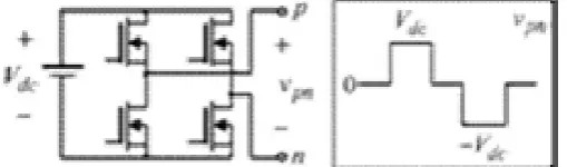
When the dc-link voltage of a single H-bridge module is Vdc, the output voltage vpn has three states, i.e., Vdc, 0,
Madhuranthaka et al., International Journal of Advanced Research in Computer Science and Software Engg. 8(4) ISSN(E): 2277-128X, ISBN: 978-93-87396-07-4, pp. 66-70
Fig. 2. Unipolar and phase shift modulation for single H-bridge module.
Fig. 3. Output voltage of a single H-bridge module
Fig. 4. One-by-three configuration MLCI.
as shown in Fig. 3. By adopting the concept of a switching function, it can be represented as
where Sp is a switching function and p can be replaced with a, b, or c, which represent the phases.
Fig. 4 shows a simple one-by-three configuration MLCI. For voltage vector space analysis, the main concept is derived from this simple topology, and then, it is expanded to more levels. In Fig. 4, there are two neutral points s and n
in the MLCI. Here, the voltage between the output point of each phase and the neutral point n is defined as the pole voltage. The pole voltages are represented as van, vbn, and vcn. The voltage between the output point of each phase and the
load side neutral point s is specified as the phase voltage. The phase voltages include vas, vbs, and vcs. By using this
concept, the voltage between the two neutral points is defined as vsn and can be written as
III. PROPOSED MODULATION TECHNIQUE
In Section II, the maximum synthesizable voltage in the linear modulation range was evaluated under the unbalanced dc links. In this section, a method is proposed to realize the maximum modulation index in the linear modulation range under these conditions.
A. Traditional Offset Voltage Injection Method
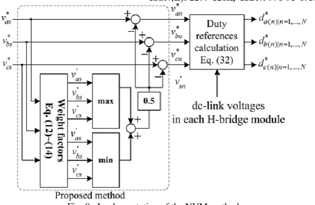
Fig. 8. Implementation of the NVM method
-references to implement various PWM schemes in carrier-based PWM by using the fact that line-to-line voltages are applied to a three-phase load [43], [44]. For example, the offset voltage vsn∗ is injected to the phase voltage
references vas∗, vbs∗, and vcs∗to implement carrier-based SVPWM as in
Then, the pole voltage references van∗, vbn∗, and vcn∗, which will be converted to PWM duty references, are
However, the aforementioned technique may not maximize the linear modulation range in MLCI undergoing unbalanced dc-link conditions.
B. Duty Calculation
In Fig. 8, the final voltage references are entered to the duty reference calculation block. In this block, the duty references of each H-bridge module are calculated as follows:
The calculated duty references are compared to PS carriers to generate gating signals, as shown in Fig. 10. It should be noted that the duty references for each H-bridge in each phase are shared in the PS modulation.
IV. MATLAB DESIGN OF CASE STUDY AND RESULTS
Madhuranthaka et al., International Journal of Advanced Research in Computer Science and Software Engg. 8(4) ISSN(E): 2277-128X, ISBN: 978-93-87396-07-4, pp. 66-70
Fig.14.Simulink model of conventional SVPWM technique
Fig.15.Performance of conventional SVPWM technique
Fig.17.Performance of traditional NVM.
VI. CONCLUSION
The NVM technique for MLCIs under unbalanced dc-link conditions has been proposed in this paper. In order to analyze the maximum synthesizable voltage of MLCIs, the voltage vector space has been analyzed using the switching function. From the analysis, the maximum linear modulation range was derived. The proposed NVM technique is applied to achieve the maximum modulation index in the linear modulation range under an unbalanced dc-link condition as well as to balance the output phase voltages. Compared to the previous methods, the proposed technique is easily implemented and improves the output voltage quality under unbalanced dc-link conditions. Both simulations and experimental results based on the IPM motor drive application verify the effectiveness of the proposed method.
REFERENCES
[1] J. Rodriguez, J.-S. Lai, and F. Z. Peng, ―Multilevel inverters: A survey of topologies, controls, and applications,‖ IEEE Trans. Ind. Electron., vol. 49, no. 4, pp. 724–738, Aug. 2002.
[2] H. Abu-Rub, J. Holtz, J. Rodriguez, and G. Baoming, ―Medium-voltage multilevel converters—State of the art,
challenges, and requirements in in-dustrial applications,‖ IEEE Trans. Ind. Electron., vol. 57, no. 8, pp. 2581– 2596, Aug. 2010.
[3] J.-S. Lai and F. Z. Peng, ―Multilevel converters—A new breed of power converters,‖ IEEE Trans. Ind. Appl.,
vol. 32, no. 3, pp. 509–517, May/Jun. 1996.
[4] M. Malinowski, K. Gopakumar, J. Rodriguez, and M. A. Perez, ―A survey on cascaded multilevel inverters,‖
IEEETrans. Ind. Electron., vol. 57, no. 7, pp. 2197–2206, Jul.2010.
[5] J. Rodriguez, L. G. Franquelo, S. Kouro, J. I. León, R. C. Portillo,A. M. Prats, and M. A. Perez, ―Multilevel