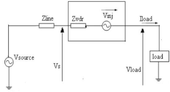
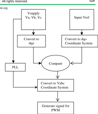
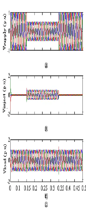
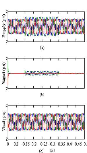
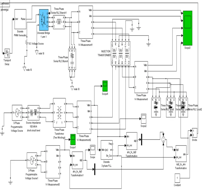
MODELING AND SIMULATION FOR VOLTAGE SAGS/SWELLS MITIGATION USING DYNAMIC VOLTAGE RESTORER (DVR)
Full text
Figure
Related documents
Patent 3,113,979 Positional isomerisation and isomerisation between alkyl substituents are produced in a single stage process by the use of a catalyst consisting of
In 2009 NTRU cryptosystem has been approved for standardization by the institute of electrical and electronics engineers (IEEE). These mathematicians contact with each other
Of these, 34 transcripts were associated with 53 eQTL (20% of the transcripts segregating among the three data sets), 22 in the female data set (Table 4A), 12 in the male data
They are the subjects’ perceptions of rural life and rural persons; the perceived costs of living in a rural environment and strategies employed to defray those costs; the
Although we favor the notion that the two actin-bind- ing domains of Sac6p do bind to the same site on actin, we suggest there are differences between the two do-
I think this view is mistaken since Feyerabend disagrees with Popper’s understanding of quantum theory (what he would later call “pompous declarations and sophomore
BAU: Business as usual; BPMS: Business Process Management System; BSC: Balanced Scorecard; EC: Executive Committee; IMC RBNQA: Indian Merchant Chambers: Ramakrishna Bajaj
Conclusions: Combination and ethanol were the most effective sclerosants in terms of highest success rates and lowest complication rates, and sclerosant volume per lesion volume had
