OPTIMIZATION AND CHARACTERIZATION OF NEW MATERIALS TO ENHANCE PERFORMANCE OF POLYMER SOLAR CELLS
Andrew Stuart
A dissertation submitted to the faculty of the University of North Carolina at Chapel Hill in partial fulfillment of the requirements for the degree of Doctor of Philosophy in the Department of Chemistry.
Chapel Hill 2012
ii
ABSTRACT
Andrew Stuart: Optimization and Characterization of New Materials to Enhance Performance of Polymer Solar Cells
(Under the direction of Dr. Wei You)
Conjugated polymer solar cells have steadily grown in efficiency, from less than 1% to over 10% in less than two decades. They have the potential to be the next major energy source due to lightweight, flexible and inexpensive materials. However, the main stumbling block to full scale adoption of polymer solar cells is the still relatively low power conversion efficiency. Researchers are currently addressing this issue by designing new materials and device structures that can improve solar cell performance.
In this report, we focused on designing and characterizing new polymers and device structures for polymer solar cells. We focus specifically on the recent discovery of effects of substituents on the conjugated backbone and how it affects not only photovoltaic response, but also charge recombination and device morphology. Further collaborations with experts of complementary expertise in the field have allowed us to zero in on specific effects fluorine substituents have on polymer stacking, domain organization with PCBM, and polymer/PCBM miscibility. Our findings have helped us to understand the influence these substituents play on photovoltaic polymers and will help us to design new higher performance materials in the near future.
iii
iv
ACKNOWLEDGMENTS
First and foremost I would like to thank Dr. Wei You for his guidance, attitude, and encouragement which provided me with a great environment to conduct my research. Next I would like to thank my committee members, Prof. Cahoon, Prof. Meyer, Prof. Papanikolas, Prof. Samulski and Prof. Sheiko, for their support and assistance in my research and in completing this dissertation.
v
TABLE OF CONTENTS
LIST OF TABLES………..…….viii
LIST OF FIGURES………...ix
Chapter 1. Introduction……..………...……….……....1
1.1. Background………...……….1
1.2. History and Development of Organic Photovoltaics...……….3
1.3. Polymer Solar Cell Basics…………...……….7
1.4. The Energy Conversion Process………...…………..9
1.4.1. Light Absorption……….………...……...9
1.4.2. Exciton Generation and Splitting….………...………….10
1.4.3. Creation of Free Charge Carriers and Charge Collection…….…....…….11
1.5. Device Morphology and Characterization………...…...………12
1.6. Improving Performance of Polymer Solar Cells………14
1.6.1. Improving PSCs by Addition of Constituents to the Polymer Backbone..14
vi
2. Fluorine Substituents Reduce Charge Recombination and Drive
Structure and Morphology Development in Polymer Solar Cells.……...…….17
2.1. Introduction………...……….17
2.2. Polymer Synthesis, Optical and Electrochemical Properties.………19
2.3. Photovoltaic Properties………...………..21
2.3.1. Open Circuit Voltage (Voc)………...22
2.3.2. Short CircuitCurrent (Jsc)………..23
2.3.3. Fill Factor (FF)………..24
2.4. Charge Recombination Studies……….…………...………25
2.5. Device Morphology…..………...……….28
2.5.1. GIWAXS Analysis……….29
2.5.2. R-SoXS Analysis………...30
2.5.3. Polymer:PCBM Miscibility Measurement with STXM ………..….……34
2.6. Conclusions………...………...37
2.7. Experimental Section………...……….37
3. Fluorine Substituted Conjugated Polymer Yields 7% Efficiency and Exhibits Remarkable Insensitivity to Induced Morphological Changes.………..…..43
3.1. Introduction………...………43
3.2. Polymer Synthesis………...…….46
3.3. Optical and Eletrochemical Properties……...……….47
3.4. General Photovoltaic Properties…………...………..49
vii
3.5.1. Characterization of PBnDT-FTAZ Morphologies with GI-WAXS……..55
3.5.2. Characterization of Morphology with R-SoXS……….57
3.5.3. Miscibility of PCBM and PBnDT-FTAZ with STXM……….………….62
3.6. Conclusions………...………..63
3.7. Experimental Section………...……….64
4. Transparent Nanoparticle Thin Films with Substantial Porosity for Enhanced Hole Collection and Transport for Polymer Solar Cells…………...…….68
4.1. Introduction………...………68
4.2. Nanoparticle Film Synthesis and Formation ...………70
4.3. Nanoparticle Film Infiltration and Characterization ...………75
4.4. Nanoparticle Films in Polymer Solar Cell Devices ………...……79
4.5. Conclusions………...………….80
4.6. Experimental Section………...………...81
5. Conclusions and Future Research Opportunities……...………..………83
5.1. Conclusion………...……….…………...83
5.2. Future Research Opportunities for Polymer Solar Cells………84
5.2.1. Mesoporous Oxide Films as a Platform for Functional Electrodes….…..84
5.2.2. New Acceptor Materials with Complementary Light Absorption….…....86
APPENDICES………...….……….…88
viii
LIST OF TABLES Table
2-1 Molecular Weight, HOMO level and Optical Properties.……...………..20 2-2 PV Response and SCLC Mobility of 1:1 Polymer:PC61BM.……...……….21
ix
LIST OF FIGURES Figure
1-1 Diagrams of device architectures……....……….……...……3
1-2 SEM micrograph of a nanoparticle oxide film used in DSSC devices …...5
1-3 BHJ Device Structure and Chemical Structures………...……….….…….6
1-4 Typical I-V curve of a polymer solar cell under illumination…...8
1-5 Light absorption spectra and coefficients………....………...…...……...….10
1-6 TEM images of Polymer:PCBM Bulk Heterojunction Morphology ..………...14
2-1 PBnDT-DTBT, -DTfBT and -DTffBT Polymer Structures …….….…………...18
2-2 UV-Vis and Fluorescence of DTBT based polymers…...………...….20
2-3 Fluorine concentration and thickness vs. Voc, Jsc, FF and η.….….………...…....25
2-4 Scaling exponent vs. voltage and FF vs. light intensity..………...……….…….27
2-5 GIWAXS data for DTBT polymers..……….………30
2-6 R-SoXS scattering profiles and scattering contrast for DTffBT...……...…..33
2-7 Miscibility of PCBM in DTBT, DTfBT, and DTffBT…...……….…..36
3-1 Polymerization of PBnDT-FTAZ and PBnDT-HTAZ……...…………...………46
3-2 Solution and film UV-Vis absorption spectra and CV voltammograms.….…….48
3-3 J-V curves and IPCE for the highest performing cells for each polymer...50
3-4 J-V curves for FTAZ devices processed from CB, DCB, and TCB………….…53
3-5 GI-WAXS out of plane, Jsc, polymer crystals scattering intensity…………..…..56
3-6 R-SoXS scattering of blend films……….……….59
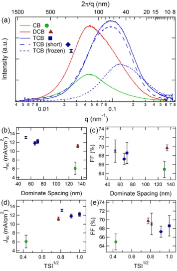
3-7 Jsc and FF as functions of dominate domain d-spacing ………...……...61
x
4-1 A cross section of a typical BHJ PSC with good morphology.……….69
4-2 A cross section of a PSC utilizing a mesoporous nanoparticle electrode.……….70
4-3 FESEM of nanoITO films prepared without and with a polymer.…………...….72
4-4 Cross-sectional FESEM of NiO nanoparticle thin films…………..……….72
4-5 FESEM of NiO nanoparticle thin films…………..………..………….73
4-6 FESEM of defects in nanoNiO films………..………..……….74
4-7 FESEM of nanoITO infiltrated with P3HT and PCBM ………....…..75
4-8 FESEM and EDS of infiltrated nanoITO thin films.…………...………..76
4-9 Raman shift of a nanoITO film infiltrated with P3HT……….….77
4-10 Secondary ion mass spectrometry of NanoNiO films………..…………..78
4-11 Diagram of a mesoporous solar cell device….………..79
5-1 Surface initiated conjugated polymerization………...……….………….…85
CHAPTER 1
Introduction
1.1 Background
2
Since the first inorganic solar cell was made in Bell Labs in 1954,1 thick, inflexible, highly processed inorganic materials have dominated the field with high power conversion efficiencies (PCE or η). Inorganic based single junction solar panels have yielded efficiencies from 8% for lower cost materials, to 25% efficiency2 for single crystalline Silicon based modules. However, the main aggravating factor to full-scale adoption of PV energy sources is the high cost of materials and processing costs3 needed to produce them. While economies of scale and process engineering have brought these costs down significantly, it may be necessary to employ a paradigm shift in the materials and processing of solar panels in order to make solar energy competitive with other energy sources.
1.2. History and Development of Organic Photovoltaics The field of organic photovoltaics
observed photocurrent being published by this initial report, progress was slow
the early 1980’s. These devices consisted of a single organic layer, typically a dye or fused ring structure, which acted as the active layer. The main stumbling block in the field was that the photocurrent achieved was dependent on a creating a large bias between the two working electrodes by using materials of different work functions. This barrier was overcome in the late 1970s and published in 1986 by Tang, with the i
bilayer device.7
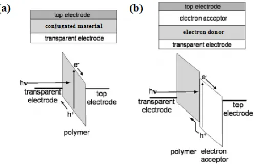
Figure 1-1. Diagrams of device architecture and function of: (a) single layer organic solar cell device; (b) bilayer solar cell device.
16, Copyright 2004 American Chemical Society.
3
istory and Development of Organic Photovoltaics
The field of organic photovoltaics can be traced back to a report of the first observed photocurrent being published by Kallman and Pope in 19606. However, after this initial report, progress was slow yielding devices achieving only 0.1% efficiency by the early 1980’s. These devices consisted of a single organic layer, typically a dye or fused ring structure, which acted as the active layer. The main stumbling block in the nt achieved was dependent on a creating a large bias between the two working electrodes by using materials of different work functions. This barrier was overcome in the late 1970s and published in 1986 by Tang, with the inception of the
Diagrams of device architecture and function of: (a) single layer organic solar cell device; (b) bilayer solar cell device. Reprinted with permission from Reference 16, Copyright 2004 American Chemical Society.
can be traced back to a report of the first However, after yielding devices achieving only 0.1% efficiency by the early 1980’s. These devices consisted of a single organic layer, typically a dye or fused ring structure, which acted as the active layer. The main stumbling block in the nt achieved was dependent on a creating a large bias between the two working electrodes by using materials of different work functions. This barrier nception of the
4
Tang reported a device made of a copper phtalocyanine (CuPC) layer (see Figure 1-3) followed by a perylene tetracarboxylic derivative layer sandwiched between two electrodes, yielding a PCE of 0.95% and fill factor (FF) of 65%. What made this device so revolutionary was the new concept of using two layers, one with an n-type and one with a p-type material. These layers formed a junction where excited electron/hole pairs could easily separate and then travel to the cathode and anode, respectively. This n/p-type material structure is the foundation with which all successful organic photovoltaics have been built from since.
5
Figure 1-2. SEM micrograph of a nanoparticle oxide film used in DSSC devices
Arguably one of the most important concepts introduced into these devices is the nanoparticle oxide layer as seen in figure 1-2, which facilitates electron collection and transport through a network of anatase TiO2 nanoparticle, greatly increasing the surface area and thus the total volume of the active layer adsorbed dye. Recent progress in these devices has evolved into the more stable solid state DSSC devices which replaces the liquid electrolyte with solid hole transporting material11,12 and the use of porphyrin based dyes with much broader light absorption spectra10.
Figure 1-3. (a) Structure and device function Chemical structures of: (b) CuPc, (c) MDMO
PC61BM. Reprinted with permission from Reference 16, Copyright 2004 American
Chemical Society.
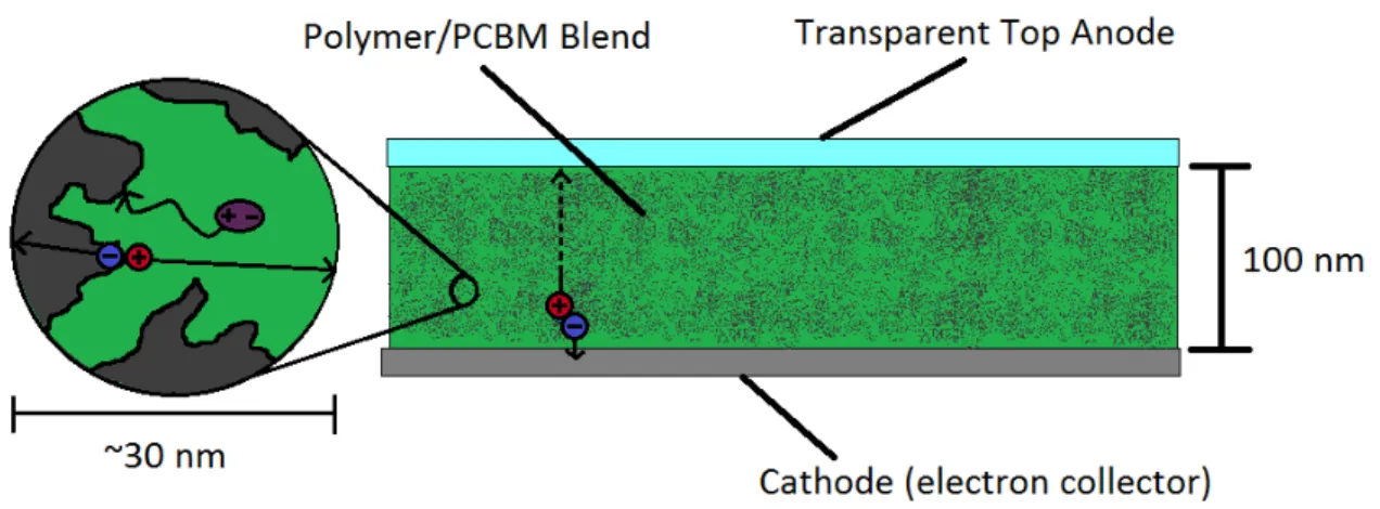
The discovery of the BHJ proved to be a pivotal step in the development of high performance PSCs. A BHJ is formed by combining both PCBM and polymer into a common solvent, then casting the solution into a thin layer onto an electrode allowing the solvent to evaporate
PCBM form a unique bi-continuous phase morphology which allows holes and electrons to transport to the anode and cathode, respectively. Additi
(when compared to bilayer devices) of the donor and acceptor materials greatly increases the surface area between the two phases which enhances the charge separation efficiency.18,19
After the discovery of the BHJ in more promising material, poly(3
6
and device function of a BHJ solar cell and morphology. Chemical structures of: (b) CuPc, (c) MDMO-PPV, (d) MEH-PPV, (e) P3HT and (f)
BM. Reprinted with permission from Reference 16, Copyright 2004 American
The discovery of the BHJ proved to be a pivotal step in the development of high performance PSCs. A BHJ is formed by combining both PCBM and polymer into a common solvent, then casting the solution into a thin layer onto an electrode allowing the solvent to evaporate.15-17 During this evaporation process, the polymer and
continuous phase morphology which allows holes and electrons to transport to the anode and cathode, respectively. Additionally, the
large-(when compared to bilayer devices) of the donor and acceptor materials greatly increases the surface area between the two phases which enhances the charge separation
After the discovery of the BHJ in 1995, researchers shifted their PSC efforts to a more promising material, poly(3-hexylthiophene) (P3HT). Over the next ten years, P3HT BHJ solar cell and morphology. PPV, (e) P3HT and (f) BM. Reprinted with permission from Reference 16, Copyright 2004 American
The discovery of the BHJ proved to be a pivotal step in the development of high performance PSCs. A BHJ is formed by combining both PCBM and polymer into a common solvent, then casting the solution into a thin layer onto an electrode and During this evaporation process, the polymer and continuous phase morphology which allows holes and electrons -scale mixing (when compared to bilayer devices) of the donor and acceptor materials greatly increases the surface area between the two phases which enhances the charge separation
7
was studied extensively and through optimization of material synthesis and morphology control achieved world record efficiencies of 5%.20-23 While this was a remarkable achievement for polymer solar cells, efficiency enhancement of P3HT plateaued due to the inherently large band gap of the polymer. Since 2005, researchers have focused on synthesizing new low band gap polymers, and have successfully raised the PCE of polymer based photovoltaics to over 7%.24-27 Looking at this rapid acceleration of world record efficiencies for PSCs, the future of the field appears to be quite promising.28
1.3. Polymer Solar Cell Basics
A typical polymer solar cell is made up of two electrodes, a transparent anode and metal cathode, sandwiching the BHJ photoactive layer as in figure 1-3(a). Upon construction of a solar cell, the single most parameter for characterizing performance is the power conversion efficiency. The PCE (η) is defined as the ratio between the input power, or power that is incident on the device (Pin), and the output power, or power
delivered by the device (Pout).
(1)
Pin is also referred to as the solar irradiance and is typically measured in units of mW/cm2.
Pout is experimentally determined by measuring the current density (Jsc) vs. voltage (V)
curve under illumination, and finding the maximum power point (MPP) of the curve (the point at which the product of Jsc and V is maximized.) Pout is also defined as the product
of the short circuit current (Jsc), open circuit voltage (Voc), and fill factor (FF).
Jsc is the amount of photocurre
and Voc is the bias required to prevent all charges from leaving the solar cell. The
the ratio between the area of the defined mathematically as:
where Jmpp and Vmpp are the value of current density and voltage at the maximum power
point, respectively. The determination of the MPP and more easily understood graphically in
Figure 1-4. Typical I-V curve of a polymer solar cell under illumination.
8
is the amount of photocurrent produced when there is no applied field to the device is the bias required to prevent all charges from leaving the solar cell. The
area of the dotted rectangle and solid rectangle in figure 1
(3)
are the value of current density and voltage at the maximum power point, respectively. The determination of the MPP and the other variables
more easily understood graphically in Figure 1-4:
V curve of a polymer solar cell under illumination.
nt produced when there is no applied field to the device is the bias required to prevent all charges from leaving the solar cell. The FF is in figure 1-4 and is
9 1.4. The Energy Conversion Process 1.4.1. Light Absorption
10
Figure 1-5. Light absorption spectra and coefficients of several photovoltaic materials in comparison with standard AM 1.5 solar spectrum. Reprinted with permission from Reference 29, Copyright 2007 American Chemical Society.
1.4.2. Exciton Generation and Splitting
11
nm.33 However, experts in the field are in agreement that increasing the surface area between the donor and acceptor materials suppresses geminate recombination and greatly enhances Jsc. In bilayer devices, the interfacial area is very small and many excitons do not reach the interface, yielding low photocurrent.34,35 The ubiquity of the BHJ is due to the fact that the two components, polymer and PCBM, are mixed in solution and can form a continuous high surface area interface which dramatically increases the amount of exciton splitting. Organization of the polymer and PCBM phases in the BHJ, also known as the active layer morphology, can change dramatically depending on the film formation conditions. Good device morphology will provide a polymer/PCBM interface within an exciton’s diffusion length allowing the dissociation of all excitons generated by light absorption. Upon reaching an interface, the exciton will split in an exceptionally fast and efficient process36 provided there is enough driving force between the LUMO of the polymer and LUMO of the PCBM.13,37
1.4.3. Creation of Free Carriers and Charge Collection
12
The transport of the free charges is facilitated by the built in voltage caused by the offset of the work functions of the two electrodes. However, the free charge carriers require a continuous pathway to the electrode in order to be incorporated into the photocurrent. This is a potential drawback of the BHJ structure, as poor mixing of material domains can lead to charges being trapped. Additionally, long winding pathways of polymer and PCBM interfaces lead to a higher probability of electrons and holes from different excitons to recombine which is referred to as bimolecular recombination. It is therefore very important to create device morphology with a large interfacial surface area between the donor and acceptor (mitigate geminate recombination) but with continuous pathways for free carriers to transport (mitigate bimolecular recombination). Through this optimized morphology, the photocurrent of the solar cell is maximized. Charge transfer into the electrode is the final non-trivial step before the charge can be incorporated into the photocurrent. Matching the electrode work function well to the HOMO of the donor and LUMO of the acceptor is necessary in order to achieve good ohmic contact that will result in minimal losses. Interfacial layers41 and wide bandgap oxides42 have been used to facilitate the charge injection process.
1.5. Device Morphology and Characterization
13
morphology. Initially, morphology was studied indirectly, by constructing solar cell active layers with different solvents, concentrations, weight ratios and thermal annealing conditions, and then observing the effect on power conversion efficiency. Studies34,43-45 have shown how important solvent selection and mixing can be on device morphology. Thermal annealing can greatly affect the organization of the active layer, especially in devices based on P3HT:PCBM.20,46,47 Other variables that affect morphology include using solvent additives,48 polymer molecular weight and structure49, and solvent annealing.17,20
14
Figure 1-6. TEM images of Polymer:PCBM Bulk Heterojunction Morphology. The darker regions of higher density PCBM clusters.
1.6. Improving Performance of Polymer Solar Cells
There are a number of different aspects of polymer solar cells that can be optimized in order to improve power conversion efficiency. These range from new monomer and polymer structures to improve hole transport and light absorption, novel additives and post processing steps to enhance morphology, to hybrid organic/inorganic devices that can increase absorption. The scope of the work in this dissertation will focus on the effects of subtle changes to constituents on two conjugated polymer series, and using a new transparent oxide structure to enhance photocurrent.
1.6.1. Improving PSCs by Addition of Constituents to the Polymer Backbone
15
absorption, affecting HOMO/LUMO energy levels, the band gap and intramolecular charge transport. A good conjugated backbone will make the polymer chain planar, have good anchoring points for side chains and constituents, and allow easy control of the electronic HOMO/LUMO levels. Rational design of the conjugated backbone has yielded high performance polymers with broad light absorption and great charge transport. Side chains can affect polymer solubility, charge transport and donor/acceptor interactions53 which makes them important to consider when synthesizing new polymer materials. Longer aliphatic chains increase polymer solubility while shorter chains enhance intermolecular hole transport. Side chain branching can be a good compromise between good solubility and allowing chains to pack closer. The majority of the work in this dissertation will focus on the effect of the addition of substituents to conjugated polymers. Substituents can have a dramatic effect on the properties of conjugated polymers and photovoltaic properties of PSCs. Recently they have been shown to be useful in tweaking electronic levels and device performance of high performance polymers.54-56 The ultimate effects stemming from constituent substitution are still not fully understood, which presents an interesting opportunity for more detailed study.
16
1This chapter is reproduced in part with permission from: Andrew Stuart, Huaxing Zhou, John R.
Tumbleston, Wentao Li, Harald Ade, and Wei You. “Fluorine Substituents Reduce Charge Recombination and Drive Structure and Morphology Development in Polymer Solar Cells” Manuscript in Preparation, 2012
CHAPTER 2
Fluorine Substituents Reduce Charge Recombination and Drive Structure
and Morphology Development in Polymer Solar Cells
12.1. Introduction
Fluorine atoms substituted directly to the backbone of conjugated polymers have shown great promise in enhancing the efficiency of polymers based bulk heterojunction (BHJ) solar cells.27,56,59-66 For example, fluorine substituents have been identified as the single performance-enhancing factor in three of the highest performing polymers.27,59-61 A detailed comparison of these three polymers and their non-fluorinated analog has been analyzed by a recent review article.66 However, the cause for the efficiency improvement varies noticeably, depending upon specific systems. It is generally true that electron-withdrawing nature of these fluorine substituents, when directly on the conjugated backbone, lowers the HOMO energy level of conjugated polymers. This can translate into an enhanced open circuit voltage (Voc) in related BHJ solar cells, which essentially
accounts for the efficiency increase in certain systems.56,59,60,64 However, in some other reported systems,27,61,63 it appears that fluorinated polymers also demonstrate noticeably better short circuit current (Jsc) and/or Fill Factor (FF) in their BHJ devices than those of
18
warrants further investigation. More importantly, the improvement on Jsc and/or FF has
been the dominating factor in the efficiency enhancement in these systems, as opposed to the Voc enhancement as the major boost for efficiency in other systems.56,59,60
Thereforethe peculiar “fluorine” impact has been under intensive research, aiming to uncover the underlying working principles.
As our attempt to further understand the “fluorine” impact, we selected one such system, poly[benzo[1,2-b:4,5-b′ ]dithiophene-alt-5,6-difluoro-4,7-dithien-2-yl-2,1,3-benzothiadiazole] (DTffBT) (“2F”) and its non-fluorinated analogue, PBnDT-DTBT (“0F”), for an in-depth study. In our original report,55 we found the fluorinated polymer (“2F”) not only exhibited an increased Voc, but also enhanced Jsc and FF in its
BHJ devices. To complete this series, we further synthesized a new polymer with a singly substituted fluorine, PBnDT-DTfBT (“1F”), and carefully investigated this polymer together with doubly and non-fluorinated analogs in a comparative manner (see Figure 2-1). In this contribution, we show how increasing the concentration of fluorine atoms boosts the performance of conventional photovoltaic characteristics (Voc, Jsc, and FF) in
this series of polymers. Further, we reveal that these fluorine atoms reduce bimolecular recombination through improved polymer organization, a purification of polymer-rich and fullerene-rich domains, and a reduction in molecular miscibility. Both the
19
recombination and morphological and structural changes are characteristic of the “fluorine”
impact in this series of polymers.
2.2. Polymer Synthesis, Optical and Electrochemical Properties
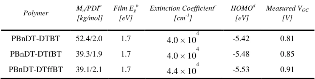
Monomers were synthesized as previously reported for both DTBT and DTffBT55 while detailed DTfBT monomer synthesis is described in the Supporting Information (See Appendix 2). Previous studies have shown that polymer molecular weight and side chain size and positioning can greatly affect the photovoltaic response of devices.53,67,68 With this polymer series, we used the exact same side chain structure for each polymer and optimized the polymerization and purification of each to yield similar molecular weight (Mn) and polydispersity index (PDI), as seen in Table 2-1.
20
Table 2-1. Key Polymers Properties: Molecular Weight, HOMO level and Optical Properties
Polymer Mn/PDI
a
[kg/mol]
Film Egb [eV]
Extinction Coefficientc [cm-1]
HOMOd [eV]
Measured VOC [V]
PBnDT-DTBT 52.4/2.0 1.7 4.0 × 10⁴ -5.42 0.81
PBnDT-DTfBT 39.3/1.9 1.7 4.0 × 10⁴ -5.48 0.85
PBnDT-DTffBT 39.1/2.1 1.7 4.4 × 10⁴ -5.53 0.91
a) Determined by GPC in 1,2,4-trichlorobenzene at 150°C.
b) Band gap calculated from the onset of the absorption of the solid film. c) Measured from film absorption spectra at λmax
d) Measured by cyclic voltammetry
500 600 700 800 900
1x10⁴ 2x10⁴ 3x10⁴ 4x10⁴ 5x10⁴ M o la r A b so rp ti v it y ε (c m -1 ) Wavelength (nm) DTBT DTfBT DTffBT N o rm a liz e d F lu o ro e s c e n c e ( A .U .)
21
Similar neat thin films of all three polymers were deposited onto a glassy carbon electrode and scanned with cyclic voltammetry to discern any differences in electrochemical ionization potentials. Examination of voltammograms for each of the polymers (see supporting Information) shows that the HOMO energy level appears to scale with increasing fluorine concentration. HOMO levels for DTBT and DTffBT are summarized in Table 2-1 and match well with previous results, while the HOMO level of DTfBT falls right in the middle at -5.48 eV.
To summarize this section, all three polymers appear to possess very similar intrinsic polymer properties, which is important to note when comparing photovoltaic response and morphology of devices made from each of the polymers. The only discernible difference found in the intrinsic properties is the slight increase in HOMO level as more fluorine atoms are introduced to backbone.
2.3. Photovoltaic Properties
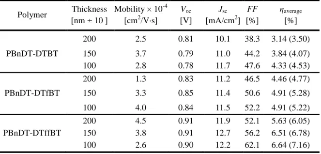
Table 2-2. PV Response and SCLC Mobility of 1:1 Polymer:PC61BM
Polymer Thickness [nm ± 10 ]
Mobility × 10-4 [cm2/V·s]
Voc
[V]
Jsc
[mA/cm2] FF [%]
ηaverage
[%] 200 2.5 0.81 10.1 38.3 3.14 (3.50)
PBnDT-DTBT 150 3.7 0.79 11.0 44.2 3.84 (4.07)
100 2.8 0.78 11.7 47.6 4.33 (4.53) 200 1.3 0.83 11.2 46.5 4.46 (4.77)
PBnDT-DTfBT 150 3.3 0.85 11.4 50.6 4.91 (5.28)
22
Photovoltaic devices were constructed and optimized in a typical fashion, by spin casting a blended solution using a device structure of ITO/PEDOT:PSS/ polymer:PC61BM/Ca/Al. After numerous optimization trials, a 1:1 weight ratio was found
to yield the best results with a concentration of 20 mg/mL in 1,2-dichlorobenzene. Once this optimal solution composition was found, solar cells were made with active layer thicknesses of 100, 150 and 200 nm to flesh out any thickness dependence of their photovoltaic characteristics. Hole mobility, which has been shown to affect device function,20,47 was measured by Space Charge Limited Current69 (SCLC). Hole mobility did not appear to vary much between each of the devices supporting that the incorporation of Fluorine on the BT unit does not significantly affect hole transport. I-V curves were measured under AM 1.5 conditions and typical photovoltaic characteristics for the polymers are displayed in Table 2-2. Analysis of the table reveals both thickness dependence within each polymer series, and fluorine concentration dependence, manifested most significantly in JSC and FF. Figure 2-3 can be used as a good graphical
aid to visualize the influence of device thickness and fluorine concentration. Below, we discuss in detail each of the three performance parameters that dictate device performance, Voc, Jsc, and FF.
2.3.1. Open Circuit Voltage (Voc)
23
reorganizational energy characterized by the Stokes shift.71 Table 2-1 shows that the HOMO level of the polymers range from -5.4 eV for DTBT to -5.5 eV for DTffBT. We attribute this difference to the observed enhancement in Voc with increasing fluorine
concentration, but to be sure we have attempted to quantify possible loss mechanisms commonly observed in Voc. The Stokes shift was observed to be ~50nm for all three
polymers indicating no polymer reorganizational losses. Additionally, looking at Figure 2-3 (a), the Voc is independent of active layer thickness, which indicates space charge
does not appear to play significant role as a loss mechanism of the Voc. The increase in
Voc seems to originate solely from the increased intramolecular charge transfer caused by
the addition of Fluorine atoms to the polymer backbone. However, this slight increase in Voc cannot fully account for the large increases observed in power conversion efficiency
as fluorine concentration is increased.
2.3.2. Short Circuit Current (Jsc)
Looking at the trends in the values of Jsc for each of the polymers in Table 2-2 (b),
there appears to be a significant effect stemming from both device thickness and fluorine concentration. For both of the fluorinated species, Jsc does not appear to vary
significantly as thickness is increased, while the DTBT series is characterized by a dramatically increasing drop in current. Additionally, there appears to be a trend of enhanced Jsc with increasing fluorine concentration, especially in the thicker 150 and 200
nm devices, where recombination processes are more likely to occur. Notably, at 200nm the Jsc for both of the fluorinated polymers are relatively the same, while the
24
light absorption or enhanced hole mobility, leading us to attribute the differences to charge recombination losses.
2.3.3. Fill Factor (FF)
Typically, charge recombination losses manifest most significantly in device FF where the internal electric field is weak. Looking at Figure 2-3(c), FF is not only greatly affected by active layer thickness, but also by fluorine concentration. Comparing the FF plot to the efficiency curves in plot (d), it is clear that of the three major photovoltaic parameters, FF appears to have the greatest influence on device power conversion efficiency. Most significantly, at 100 nm thickness, the fully fluorinated DTffBT exhibits the highest FF of 62% compared to only 52% and 48% for DTfBT and DTBT, respectively. This trend continues with increasing device thickness, with the non-fluorinated DTBT dropping to a mere 38% FF at 200 nm, while both non-fluorinated polymers still possess respectable fill factors.
25
Figure 2-3. Fluorine Concentration (DTBT, DTfBT, DTffBT) and Device Thickness (100nm,150nm, 200nm) are varied and their effect on (a) Voc, (b) Jsc, (c) FF and (d) η are
shown. Thickness measurements are +/- 10 nm.
2.4. Charge Recombination Studies
In order to determine which loss mechanisms are causing the noted differences in FF and efficiency, we measured photovoltaic performance under variable light intensity (Plight) between 0.2 and 1.5 suns. This technique is a simple probe for bimolecular
26
photocurrent (Jphoto) at different values of Plight, bimolecular recombination can be
quantified as a function of applied voltage by fitting a power law scaling exponent, α via,
Jphoto = β(Plight)α (1)
where β is a constant. Figure 2-4 shows a stark increase in α which represents a decrease in bimolecular recombination near maximum power point (~0.5 V) as the Fluorine density is increased. This reduction in recombination with Fluorine addition helps explain the enhanced FF as observed in Figure 2-3c and Figure 2-4b as functions of active layer thickness and light intensity, respectively. In terms of light intensity dependence, Figure 4b shows not only a higher absolute FF but also an insensitivity of FF to light intensity for DTffBT-based devices. This means that as the number of free carriers increases via a higher Plight, blends with a greater number of fluorine substituent atoms are able to stifle
recombination and avoid FF losses. Overall, the light intensity dependence of Jphoto and
FF indicates that at maximum power point, bimolecular recombination is indeed weakest in the devices with DTffBT and increases as the number of fluorine substitute atoms is reduced.
Differences in recombination are not limited to maximum power point and also influence Jsc. As the applied voltage is decreased to strengthen the internal electric field
and sweep out more of the charge carriers, α increases for all devices. There is low bimolecular recombination at short circuit conditions for the fluorinated DTffBT and DTfBT devices since α ≈ 1, while those based on DTBT only achieve minimal recombination for higher electric fields near -3 V bias. At short-circuit, α = 0.92 for DTBT-based solar cells, which indicates that Jsc is restricted due to this loss mechanism.
27
that is sensitive to the number of fluorine substituent atoms on the polymer backbone. Changes in this recombination process help explain the observed enhancement in FF when moving from DTBT to DTfBT to DTffBT-based devices.
Figure 2-4. (a) Scaling exponent vs voltage and for devices with different Fluorine concentration and 200nm thickness. (b) FF as function of light intensity.
28
losses due to geminate recombination is to apply a large reverse bias to working devices under illumination, and compare the observed saturation current (Jsat) with Jsc.74 A large
reverse bias should overcome any built in space charge and increase the drift velocity of the excitons enough to prevent geminate recombination. To characterize our devices, we applied a reverse bias up to -3 volts to reach the JSAT for each of the polymers (See
Appendix 2). The ratio of JSC/JSAT is around 80% for all three polymers, indicating
fluorine substitution plays little role in influencing geminate recombination losses.
2.5. Device Morphology
29
performance, but they also reveal morphological and structural changes imposed by the substituent atoms since blend films receive no thermal or solvent annealing treatment. 2.5.1. GIWAXS Analysis
Appendix 2) confirms this result where fibrillar structures are observed. Overall, these results indicate that addition of two fluorine substituent atoms causes a change in the polymer crystallinity and crystallite orientation of blend films. The relevance to device performance will be discussed below.
Figure 2-5. Two dimensional DTBT, and (c) DTBT polymers.
peaks labeled along with the typical scattering
2.5.2. R-SoXS Analysis
While GIWAXS provides valuable insights into the structure of the polymer/fullerene blends, it is only sensitive to the crystalline regions of the film. However, amorphous regions not probed with GIWAXS can
device function, especially since molecular miscibility has been demonstrated for many BHJ systems.80 To gain a more complete picture of film morphology, the distributions of
30
ms this result where fibrillar structures are observed. Overall, these results indicate that addition of two fluorine substituent atoms causes a change in the polymer crystallinity and crystallite orientation of blend films. The relevance to device
ance will be discussed below.
Two dimensional GIWAXS data for blend films based on (a) DTffBT, (b) DTBT, and (c) DTBT polymers. (d) In plane and out of plane sectors with the polymer peaks labeled along with the typical scattering contribution from PCBM.
While GIWAXS provides valuable insights into the structure of the polymer/fullerene blends, it is only sensitive to the crystalline regions of the film. However, amorphous regions not probed with GIWAXS can play an important role in device function, especially since molecular miscibility has been demonstrated for many To gain a more complete picture of film morphology, the distributions of ms this result where fibrillar structures are observed. Overall, these results indicate that addition of two fluorine substituent atoms causes a change in the polymer crystallinity and crystallite orientation of blend films. The relevance to device
blend films based on (a) DTffBT, (b) In plane and out of plane sectors with the polymer
31
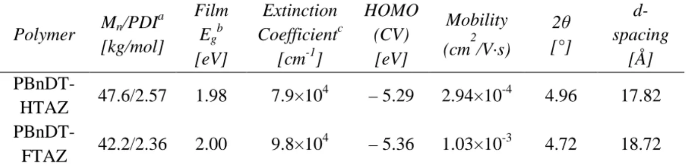
domain spacing along with relative domain purities are assessed with resonant soft X-ray scattering (R-SoXS). This technique utilizes the unique optical contrast between polymer and fullerene near the carbon 1s absorption edge (hν ~ 280 eV). Using the dispersive (δ) and absorptive (β) parts of the complex index of refraction, 1 , for the polymers and PCBM (see Appendix 2), the scattering contrast as a function of photon energy is shown in Figure 2-6a for DTffBT and PCBM. The contrast is determined by the differences in δ and β and is proportional to ∆ ∆.. Also displayed in Figure 2-6a is the contrast between polymer and fullerene with vacuum, which represents scattering due to mass-thickness variations, such as surface roughness.
32
In order to justify that the scattering peaks observed for 284.0 eV photon energy represent domain separation between polymer-rich and fullerene-rich domains, the total scattering intensity (TSI) is determined as a function of energy. This corresponds to integrating the scattering curves in Figure 2-6a and is given by:
! " #$∆ ∆%
&%' (2)
where # is the incident photon energy, %( is the material volume fraction of each domain, and '
is the illuminated volume proportional to the film thickness. Figure 2-6b shows that the energy dependence between 280 and 287 eV has approximately the same energy dependence as the contrast function of polymer:PCBM and does not follow either of the vacuum contrast functions. From this agreement, we can be confident that the scattering is a result of optical contrast between polymer-rich and fullerene-rich domains.
Figure 2-6. (a) R-SoXS scattering profiles for photon energies where the contrast between polymer and fullerene is enhanced (284.0 eV) and reduced (27
Scattering contrast for DTffBT:PCBM as function of photon energy near the carbon 1s absorption edge. Contrast of both polymer and fullerene with vacuum are also shown, which quantify mass-thickness variations such as surface roughness. The ene dependence of the total scattering intensity (TSI) matches the energy dependence of the DTffBT:PCBM contrast function supporting that the measured scatter at 284.0 eV is dominated by contrast between polymer
scattering is dominated by surface roughness which explains the absence of the broad scattering distribution at this energy in (a).
33
SoXS scattering profiles for photon energies where the contrast between polymer and fullerene is enhanced (284.0 eV) and reduced (27
Scattering contrast for DTffBT:PCBM as function of photon energy near the carbon 1s absorption edge. Contrast of both polymer and fullerene with vacuum are also shown,
thickness variations such as surface roughness. The ene dependence of the total scattering intensity (TSI) matches the energy dependence of the DTffBT:PCBM contrast function supporting that the measured scatter at 284.0 eV is dominated by contrast between polymer-rich and fullerene-rich domains. For 270.0 e scattering is dominated by surface roughness which explains the absence of the broad scattering distribution at this energy in (a).
34
Both GI-WAXS and R-SoXS reveal that fluorine substitution plays a role in the determining the structure and morphology of spincast films. To summarize, the fully fluorinated DTffBT-based blend shows greater face-on polymer crystalline structure and larger lamellar crystallites along with larger polymer/fullerene domains that are more pure. Since blends do not receive thermal or solvent annealing treatment and are merely allowed to dry in a closed petri dish after spin casting, the structure and morphology are not forced to evolve under additional driving forces. Even when cast films were not allowed to dry over a typical 12 hour period and instead were vacuum dried immediately after spin coating, similar structural and morphological differences were observed, namely that polymer crystallite orientation becomes more face on and dominate domain spacing and purity increase with fluorine substitution (see Appendix 2). For these samples, the crystallite orientation and dominate domain spacing are frozen in place and not allowed time to diffuse into a more diffuse structure. This indicates that the fluorine atoms play a fundamental role in determining the structure and morphology of the active layers.
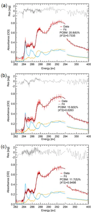
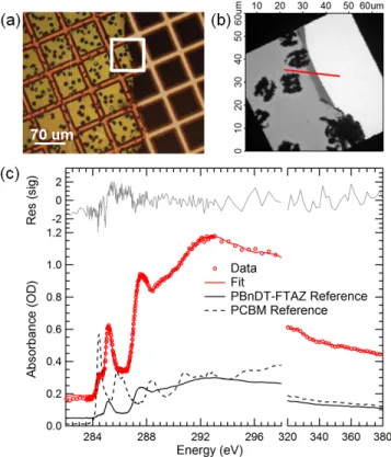
2.5.3. Polymer:PCBM Miscibility Measurement with STXM
35
matrix and quantified. Figure 2-7 shows spectroscopic line scans of the depleted polymer matrix along with linear combination fits using the pure polymer and PCBM spectra. It is found that the miscibility of PCBM in polymer is highest for DTBT at 20% and reduces to 16% and 12% for DTfBT and DTffBT, respectively. In all cases, the initial percentage of PCBM in the blend films is ~50% by weight as measured during solution preparation and confirmed on STXM measurements of non-annealed films (see Appendix 2). The trend in miscibility is in agreement with the trend in domain purity where the domain purity increases with fluorine substitution. In other words, DTBT based blends have the highest miscibility (i.e. highest molecular mixing) and therefore have the lowest domain purity.
Figure 2-7. Miscibility of PCBM in (a) DTBT, (b) DTfBT, and (c) DTffBT that were solvent annealed to equilibrium. Scanning transmission x
used to measure the film composition near large, pure PCBM crystals that form after long-term annealing. The initial PCBM percentage by weight prior to ann
is not a good predictor for the increased recombination observed. Therefore, the structure and morphology could play a very important role. A primary result of this paper is that
36
Miscibility of PCBM in (a) DTBT, (b) DTfBT, and (c) DTffBT
that were solvent annealed to equilibrium. Scanning transmission x-ray microscopy was used to measure the film composition near large, pure PCBM crystals that form after term annealing. The initial PCBM percentage by weight prior to annealing was 50%.
is not a good predictor for the increased recombination observed. Therefore, the structure and morphology could play a very important role. A primary result of this paper is that
Miscibility of PCBM in (a) DTBT, (b) DTfBT, and (c) DTffBT in thin films ray microscopy was used to measure the film composition near large, pure PCBM crystals that form after
ealing was 50%.
37
characterizing one aspect of the morphology is not sufficient to fully describe device performance.
2.6. CONCLUSIONS
In this study, a new polymer was synthesized and combined with two other to create a series of polymers with varied fluorine concentration on the BT moiety. I-V characterization showed that fluorine concentration has a small effect on VOC and JSC, but
most significantly impacts device FF and bimolecular recombination. This effect can be explained by the observed behavior changes that are caused by increasing the fluorine concentration. The fully fluorinated DTffBT-based blend shows greater face-on polymer crystalline structure and larger lamellar crystallites along with larger polymer/fullerene domains that are more pure. The higher purity, caused by the observed lower miscibility with PCBM as fluorine concentration is increased, reduces bimolecular recombination leading to improved device function. Most significantly, fluorine substitution onto the BT unit increases overall device efficiency from 4 to over 7%, scaling with increasing fluorine concentration, and may have similar effects when substituted onto similar monomers and conjugated polymers.
2.7. Experimental Section Reagents and instrumentation
38
solvents were dried when necessary and purified by distillation. Microwave assisted polymerizations were conducted in a CEM Discover Benchmate microwave reactor. Gel permeation chromatography (GPC) measurements were performed on a Polymer Laboratories PL-GPC 220 instrument (at Cornell University) The obtained molecular weight is relative to the polystyrene standard. 1H nuclear magnetic resonance (NMR) measurements were recorded either with a Bruker Avance 300MHz AMX or Bruker 400 MHz DRX spectrometer. 13C nuclear magnetic resonance (NMR) measurements were carried out with a Bruker 400 MHz DRX spectrometer. Chemical shifts were expressed in parts per million (ppm), and splitting patterns are designated as s (singlet), d (doublet), m (multiplet) and br (broad). Coupling constants J are reported in Hertz (Hz).
UV-Vis & Fluorescence Spectroscopy
39 Cyclic voltammetry
Cyclic voltammetry measurements were carried out using a Bioanalytical Systems (BAS) Epsilon potentiostat equipped with a standard three-electrode configuration. Typically, a three-electrode cell equipped with a glassy carbon working electrode, a Ag/AgNO3 (0.01 M in anhydrous acetonitrile) reference electrode, and a Pt wire counter
electrode was employed. The measurements were done in anhydrous acetonitrile with tetrabutylammonium hexafluorophosphate (0.1 M) as the supporting electrolyte under an argon atmosphere at a scan rate of 100 mV/s. Polymer films were drop-cast onto the glassy carbon working electrode from a 3 mg/mL chlorobenzene solution and dried under house nitrogen stream prior to measurements. The potential of Ag/AgNO3 reference
electrode was internally calibrated by using the ferrocene/ferrocenium redox couple (Fc/Fc+). The electrochemical onsets were determined at the position where the current starts to differ from the baseline. The highest occupied molecular orbital (HOMO) and lowest unoccupied molecular orbital (LUMO) energy levels of polymers were calculated from the onset oxidation potential (Eox ) and onset reductive potential (Ered), respectively, according to eqs. 1 and eqs. 2.
) 8 . 4 ( + −
= Eox
HOMO (eV) (1)
) 8 . 4 ( + −
= Ered
LUMO (eV) (2)
Polymer solar cell fabrication and testing
40
sheet resistance of 15Ω/□. Prior to use, the substrates were ultrasonicated for 20 minutes in 2-propanol. The substrates were then dried under a stream of nitrogen and placed in a UV-Ozone cleaner for 20 minutes. A 0.45 µm PVDF filtered dispersion of PEDOT:PSS in water (Baytron PH500) was then spun cast onto clean ITO substrates at 4000 rpm for 60 seconds and baked at 140 °C for 20 minutes yielding a thin film with a thickness of 40 nm. A 1:1 w/w blend of polymer and PCBM at 10 mg/mL was dissolved in dichlorobenzene 120 °C for overnight, filtered through a 1.0 µm poly(tetrafluoroethylene) (PTFE) filter, and spun cast between 400 – 1000 rpm for 60 seconds onto a PEDOT:PSS layer. The substrates were then left to dry at room temperature under N2 for 12 hours. The devices were finished for measurement after
41
voltage drop Vrs across the indium tin
oxide/poly(3,4-ethylene-dioxythiophene):poly(styrene sulfonic acid) (ITO/PEDOT:PSS) series resistance and contact resistance, which is found to be around 35 Ω from a reference device without the polymer layer. From the plots of J 0.5 vs. V(supporting information), hole mobilities of copolymers can be deduced from
(3)
where ε0 is the permittivity of free space, εr is the dielectric constant of the polymer
which is assumed to be around 3 for the conjugated polymers, µh is the hole mobility, V is
the voltage drop across the device, and L is the film thickness of active layer. AFM Images were taken using an Asylum Research MFP3D Atomic Force Microscope. Varied light intensity studies were performed by using neutral density filters ranging from 0.1 up to 1.0 optical density. Light intensity for each filter was calculated by the ratio of measured current of an NREL certified stardard silicon solar cell under each filter to the current collected under 1-sun condition. A total of 7 different light intensities were used as I-V curves were collected in series from each individual device.
Grazing Incidence Wide Angle X-ray Scattering (GIWAXS).
Samples for GI-WAXS were prepared on PEDOT:PSS-coated Si substrates using the same preparation conditions as devices. Measurements were taken at beamline 7.3.3 of the Advanced Light Source using a Pilatus 1M detector. A grazing incident angle of 0.15º was used where air scatter was minimized by purging the air between the x-ray source, sample, and detector with helium gas.
3 2
0 8 9
42 Resonant Soft X-ray Scattering (R-SoXS).
2This chapter is reproduced in part with permission from Reference 27 and John R. Tumbleston, Andrew
C. Stuart, Eliot Gann, Hongping Yan, Brian A. Collins, Wei You, and Harald Ade. “Insensitivity of device performance to morphology in high performance organic solar cells” Manuscript in Preparation for Advanced Materials, 2012.
CHAPTER 3
Fluorine Substituted Conjugated Polymer Yields 7% Efficiency and Exhibits
Remarkable Insensitivity to Induced Morphological Changes
23.1. Introduction
44
polymers with high photovoltaic efficiency would be desirable in addition to high performance low band gap polymers.
Poly(3-hexylthiophene) has long been the standard medium band gap polymer used in tandem solar cells, since single bulk heterojunction (BHJ) cells of P3HT blended with PCBM exhibit a reliably measured power conversion efficiency between 4% and 5%.46
However, P3HT exhibits a very high lying HOMO energy level of – 5.1 eV, which limits the Voc of the resulting photovoltaic cells to a low value of 0.6 V. Second, P3HT based BHJ cell requires either thermal or solvent annealing to reach maximum performance, a time consuming process, which is not conducive to roll to roll high throughput manufacturing. Thus, the seemingly overlooked medium band gap polymers warrant further exploration.
Research efforts in this group have recently focused on developing low band gap intramolecular charge transfer (ICT) copolymers using the design motif outlined in Fig.
1a.90,91,92
45
observed for TAZ based polymers than the benzothiadiazole based counterparts. TAZ based polymers also provide an additional advantage of incorporating solubilizing alkyl chains onto the acceptor unit, rather than on the thiophene rings on the backbone of the polymer. Alkyl chains anchored to the thiophene rings on the polymer backbone may cause steric repulsion between the adjacent monomer units. Therefore, placing the alkyl chain away from the polymer backbone on the TAZ unit allows the polymer backbone to adopt a more planar conformation. We hypothesize that this increased planarity would increase the hole mobility of the resulting polymer.
While a wider band gap is a disadvantage in that less light is harvested from the solar spectrum, the larger gap between the HOMO and the LUMO on the polymer provides an opportunity to increase the open circuit voltage.93
In order to increase the Voc while holding the band gap constant, the energy levels of both the HOMO and LUMO of the conjugated polymer must be decreased simultaneously. Thus, electron withdrawing groups would need to be added to the polymer. Fluorine has recently attracted attention as an electron withdrawing group used in high efficiency photovoltaic polymers.62
Since it is only one small atom in size, it can be introduced onto the polymer backbone without any deleterious steric effects that a larger electron withdrawing group such as a nitro or trifluoromethyl group would incur. Density functional theory calculations predicted a 0.11 eV decrease in the HOMO energy level by adding two fluorine atoms to the benzotriazole unit. Thus, the fluorinated monomer, FTAZ, was envisioned and synthesized.
46
Both polymers show an optical gap of 2.0 eV, which is even slightly bigger than that of P3HT (1.9 eV). However, the photovoltaic performance of PBnDT-HTAZ is on par with that of P3HT, with an overall efficiency of 4.3% at an active layer thickness of 230 nm. More impressive results come from the PBnDT-FTAZ:PC61BM based BHJ cells, which show a Voc of 0.79 V, a Jsc of 12.45 mA/cm2, and a very notable FF of 72.2%, leading to a highest overall efficiency of 7.1% with an active layer thickness of 250 nm. Furthermore, PBnDT-FTAZ based BHJ cells are able to achieve an efficiency of 6% at an unprecedented active layer thickness of 1 micron, and can achieve high efficiencies under a number of different solvent processing conditions. All these boast the great potential of PBnDT-FTAZ in constructing low cost, high efficiency solar cells.
3.2. Polymer Synthesis
Figure 3-1. Polymerization of PBnDT-FTAZ and PBnDT-HTAZ with a Suzuki polycondensation.
butylnonyl)benzo[1,2-b:4,5-47
b']dithiophene produced the corresponding copolymers (HTAZ and PBnDT-FTAZ, Fig. 3-1) in yields greater than 95%. Both polymers were purified by Soxhlet extraction with methanol, ethyl acetate, hexanes, and chloroform. The resulting purple solids from the chloroform fraction exhibit high and nearly identical molecular weight distributions (Table 3-1).
Table 3-1. Key optical, electrochemical and polymer properties of HTAZ and FTAZ
Polymer Mn/PDI
a
[kg/mol]
Film Egb
[eV]
Extinction Coefficientc
[cm-1]
HOMO (CV) [eV]
Mobility (cm2/V·s)
2θ [°] d-spacing [Å]
PBnDT-HTAZ 47.6/2.57 1.98 7.9×10
4
– 5.29 2.94×10⁻⁴ 4.96 17.82
PBnDT-FTAZ 42.2/2.36 2.00 9.8×10
4
– 5.36 1.03×10⁻³ 4.72 18.72 a) Determined by GPC in 1,2,4-trichlorobenzene at 150°C.
b) Band gap calculated from the onset of the absorption of the solid film. c) Measured from film absorption spectra at λmax (534 nm).
3.3. Optical and Eletrochemical Properties
48
of PBnDT-FTAZ indicates that it aggregates in solution much more strongly than PBnDT-HTAZ.
In addition to small differences in absorption spectra, the two polymers display very similar electrochemical oxidation characteristics as well (Fig. 3-2d). Cyclic voltammetry reveals reversible oxidation behavior for both polymers, with the fluorinated
Figure 3-2. Solution UV-Visible absorption spectra for a) FTAZ and b) PBnDT-HTAZ; c) Film UV-Vis absorption spectra for both polymers; d) The oxidative portion of the cyclic voltammogram for PBnDT-FTAZ and PBnDT-HTAZ. The ferrocene/ferrocenium redox couple is used as a standard (-4.8 eV) and is shifted up the Y-axis by 0.5 mA for clarity.
49
material. Both materials display HOMO energy levels at least 0.2 eV lower than the currently favored, wide band gap polymer, P3HT (– 5.1 eV), implying that a higher Voc could be obtained than that of the P3HT based devices (~ 0.6 V). The cyclic voltammetry LUMOs for PBnDT-FTAZ and PBnDT-HTAZ are -3.05 eV and -2.87 eV, respectively. In summary, despite minor differences in the aggregation properties in solution and the oxidation behavior, these polymers possess roughly identical optical and electronic properties.
3.4. General Photovoltaic Properties
Optimized photovoltaic devices were obtained by spin casting a 1:2 blend of polymer:PC61BM in 1,2,4-trichlorobenzene (TCB), and then allowing the
trichlorobenzene to evaporate slowly in a petri dish. Thickness optimizations were conducted and summarized in Table 3-2. While the optimal thickness for PBnDT-HTAZ is easily identified as around 230 nm with the highest Jsc and FF among corresponding values associated with all thicknesses studied, the optimal thickness in the case of PBnDTFTAZ is arguably estimated to be around 250 nm where the highest efficiency was obtained (7.1%) (Fig. 3-3a and 3-3b). In fact, one particular feature of the fluorinated material (PBnDT-FTAZ) is its insensitivity to changes in active layer thickness. The Jsc continuously rises as the thickness of the active layer of PBnDT-FTAZ:PC61BM BHJ
50
It is intriguing to note that PBnDT-FTAZ performs almost twice as well as PBnDT-HTAZ, though the only difference between these two polymers is the two
Figure 3-3. (a) J-V curves for the highest performing cells for each polymer. The fluorine atoms cause increases in every performance category. PBnDT-FTAZ overall performs 76% better than PBnDT-HTAZ. (b) Incident photon to current efficiency and solid film absorption of each blend of polymer:PC61BM. (c) Dependence of the FF and Jsc on the
thickness of the active layer. (d) SEM of 1 micron active layer that showed 6% power conversion efficiency (scale bar: 1 µm).
51
Table 3-2. Thickness optimizations for photovoltaic devices.
Polymer Polymer: PC61BM
Thickness [nm]
Voc
[V]
Jsc
[mA/cm2]
FF [%]
ηaverage (ηmax)
[%] PBnDT-
HTAZ
1:2 165 0.66 8.47 52.4 2.94 (3.27)
1:2 230 0.70 11.14 55.2 4.30 (4.36)
1:2 430 0.66 9.73 50.5 3.25 (3.29)
1:2 750 0.71 9.41 47.1 3.14 (3.18)
PBnDT- FTAZ
1:2 160 0.74 11.54 70.4 6.03 (6.49) 1:2 250 0.79 11.83 72.9 6.81 (7.10) 1:2 310 0.79 12.20 67.3 6.47 (6.76) 1:2 400 0.74 13.33 58.0 5.83 (6.17) 1:2 1000 0.74 13.97 54.1 5.60 (6.06)
the electron withdrawing effect of the fluorine atoms. Additionally, we also hypothesized that PBnDT-FTAZ chains may pack in a wider and possibly more ideal fashion due to the repulsive nature of the fluorine atoms, which repel hydrocarbon materials. This hypothesis was tested with X-ray diffraction spectroscopy (Table 3-1), and indeed a larger d-spacing was observed for the fluorinated polymer PBnDT-FTAZ than for the non- fluorinated material (18.6 Å vs. 17.5 Å). It is, therefore, not unreasonable to conclude that PC61BM is also kept slightly farther away from the PBnDT-FTAZ chains
52
3.5. Morphology effect on Photovoltaic Properties of PBnDT-FTAZ
Figure 3-4. (a) Current density vs. voltage under 1 Sun illumination for PBnDT FTAZ:PCBM devices processed from CB, DCB, and TCB. The inset shows the chemical structure of PBnDT-FTAZ. (b) Short
devices along with two other devices processed from TCB (number 4 and 5) that receive shorter annealing times compared to the normal TCB device (number 3). While changes are noted in the Jsc with respect to processing condition, the
all samples indicating excellent charge transport with minimal recombination.
53
(a) Current density vs. voltage under 1 Sun illumination for PBnDT FTAZ:PCBM devices processed from CB, DCB, and TCB. The inset shows the chemical
FTAZ. (b) Short-circuit current (Jsc) and (c) fill factor (
devices along with two other devices processed from TCB (number 4 and 5) that receive shorter annealing times compared to the normal TCB device (number 3). While changes with respect to processing condition, the FF remains at least 65% for all samples indicating excellent charge transport with minimal recombination.
(a) Current density vs. voltage under 1 Sun illumination for PBnDT-FTAZ:PCBM devices processed from CB, DCB, and TCB. The inset shows the chemical
54
carriers is expected. The high FF indicates that extraction of photogenerated carriers is excellent where loss of free carriers via pathways such as bimolecular recombination97 are minimal regardless of solvent choice.
Since changes in performance with solvent are primarily noted in Jsc, two other
preparation conditions are used when casting from TCB in order to broaden the parameter space of processing conditions. Reducing the drying time for TCB cast films was achieved using a larger petri dish for solvent drying (TCB (short)) and by vacuum drying (pressure = -30 in.Hg) for 10 min immediately after spin-coating (TCB (frozen)). Performance parameters are shown in Figure 3-4(b),(c) and listed in Table 3-3 for all processing conditions of this study. Interestingly, all the processing conditions show good performance above 5.8% except for blends cast from CB, where the Jsc is substantially reduced (Figure 1(b)). For all processing conditions, the FF remains above 65%. It should be noted that there are insignificant changes in absorption from UV-VIS measurements so variations in Jsc are asserted to be due to changes in internal quantum efficiency, not absorption efficiency.
Table 3-3. Average device performance with different processing conditions
Device Number Processing Condition Thickness (nm) Voc (V) Jsc
(mA/cm2)
FF (%)
PCE (%)
1 CB 270 ± 5 0.79 ± 0.01 6 ± 1 65 ± 2 3.1 ± 0.8
2 DCB 245 ± 5 0.82 ± 0.01 11.2 ± 0.4 70 ± 1 6.4 ± 0.3
3 TCB 260 ± 5 0.79 ± 0.01 12.2 ± 0.4 69 ± 2 6.6 ± 0.3
4 TCB (short) 250 ± 5 0.74 ± 0.01 11.8 ± 0.4 67 ± 1 5.8 ± 0.3