Open Access Journal
Published BY AENSI Publication
© 2017 AENSI Publisher All rights reserved
This work is licensed under the Creative Commons Attribution International License (CC BY).
http://creativecommons.org/licenses/by/4.0/
To Cite This Article: Gurneet Kaur Gill and Paramveer Singh Gill., Design and Implementation of ALU Using Vedic Mathematics Based Multiplication Unit.. Aust. J. Basic & Appl. Sci., 11(4): 100-106, 2017
Design and Implementation of ALU Using Vedic Mathematics Based
Multiplication Unit.
1Gurneet Kaur Gill and 2Paramveer Singh Gill
1Student, Chandigarh Engineering College, M.tech VLSI, Gurneet Kaur Gill, Landran, Punjab, India.
2Assistant Professor, Chandigarh Engineering College, Electronics and Communication Department, Paramveer Singh Gill, Landran,
Punjab, India.
Address For Correspondence:
Gurneet Kaur Gill, Student, Chandigarh Engineering College, M.tech VLSI, Gurneet Kaur Gill, Landran, Punjab, India.
A R T I C L E I N F O A B S T R A C T Article history:
Received 18 December 2016 Accepted 16 March 2017
Available online 25 March 2017
Keywords:
Vedic Multiplier, Arithmetic Logic Unit (ALU), DSP operations, ALU, CSA, Verilog.
Background: An ALU is the most significant building block required in arithmetic and logical functions. Multiplication unit is the key block of ALU and can be used to control many logical implementation of the circuit. Although some multiplication based algorithms are in use, the implementations of multipliers put up on Vedic mathematics have not got that much credit. The structure minimizes the complexity. The technique is helpful in reducing the computational path delay and by reutilization of resources the area overhead can be minimized to a certain extent. Objective: In this paper a vedic mathematics based multiplication unit is used to design an ALU. The Vedic mathematics based algorithm is adopted for multiplication in the projected advance in addition to carry select adder bring into play in order to improve the timing complexity as well as area overhead. Results: The proposed methodology is implemented using the Xilinx Spartan 6 FPGA and Verilog Hardware Description Language. In the proposed architecture the timing delay is improved by a significant value of approx. 62% with the slight improvement in area. Conclusion: The improvement in the timing delay allows the circuit to work faster in the digital circuits. In the future the arithmetic operations unit must be further improved in terms of area efficiency which increases its application in digital processing functions.
INTRODUCTION
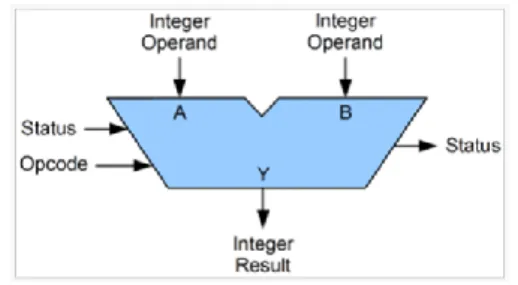
Fig. 1: Symbolic representation of ALU
Related Work:
In Rawat (2015), in this document, the multiplication unit of ALU is built by making the use of ancient formulas simply known as 16 sutras i.e. (Vedic Mathematics).The number of configurations can be made such as 2 bit, 4 bit and 8 bit multipliers using the method of Vedic approach .The encoding is in a VHSIC Hardware Description language (VHDL) and EDA tool is further used for synthesisation, on Xilinx ISE12.2i.In Begum (2016), the model and functions of a range of tasks approved out by a reconfigurable ALU are explained in. A one precision presentation representing the location of decimal point by exponent of radix, addition and subtraction of 32 bit is taken. It can be helpful in parallel processing approach and computation intensive applications. In Ravi Kishore Kodali (2014), the most common way to represent or write the floating point digits is as ((1)S)(F)(2E), where the fractional values are represented by F as well as the exponent values are shown by E. In general, mantissa value can be allotted by addition of 1 as MSB. The part containing the large value of exponent than the value could be handled; in such condition the overflow flag becomes high. In Poornima M. (2013), with the usage of formulae from Vedic mathematics multiplier is designed and outcomes are detailed in terms of area and delay consumption. In M. Senthil Kumar (2014), the synchronous vital algorithm is used, in which the transmitter as well as the receiptant are employed for a single standard of coding as well as decoding known as AES. The given structure is compare to the other one called look up table way, as area occupied by the Look-up table approach is much more along the amount of a Xilinx Spartan 3E series of FPGA. In Biswajeet Pandey (2013), in order to optimise the energy, there is a latest technique that is employed is low voltage complementary metal oxide semiconductor approach. The output evaluation shows a energy optimization as using LVCMOS12 and LVCMOS15 instead of LVCMOS 25 is 68.34% and 52.51%.In Biswabandu Jana(2014), The Co-existence of CMOS and SET (Single Electron Transistor) is the current growth in the age of superior semiconductor engineering. This document results with the tough execution of ALU (Arithmetic Logic Unit) BY employing hybrid SET-CMOS, as well as compose exercise of hybrid SET-CMOS based reversible nature logic gates. The imitation of outputs of given both cases are done with estimate of similarities and dissimilarities
made between them by means of miscellaneous advances. In this paper ALU design of 4 bit hybrid SET-CMOS
and 4 bit hybrid SET-CMOS Reversible logic gate .In Subhajit Roy(2014), the paper demonstrates a well organised and operational designing the asynchronous ALU with minimisation of delay for the execution of instructions on FPGA. By using 4 way handshaking protocol the delay can be decreased and get large pliability and execution of the arithmetical and logical unit. The design methodology counted here is asynchronous. In Priyanka Nautiyal (2015), as the need required in ALU is calculation of large number of bits therefore it is required to add cascading addition unit. But the disadvantage is that Cascaded adders cause Carry Propagation Delay (CPD) .As a result the speed decreases of the whole operation. 8 Bit, 16 Bit, 32 Bit and 64 Bit ALU is designed by modified SQRT CSLA and also implemented ALU using modified SQRT CSLA by CLA. Thus for
higher bit ALU, regular/modified SQRT CSLA, cascade methodology can be used.
Carry Select Adder:
The CSA here is basically for combating the delays that are caused due to carry calculation in ripple carry adder. In this work a 4 bit, 8 bit, 16 bit and 32 bit CSA are constructed respectively.
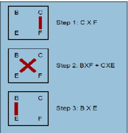
Fig. 3: Vertical and Crosswise approach.
Vedic Multiplication unit for 2*2 bit module:
The scheme is illustrated below for two, 2 bit number A and B, where A=a1a0 and B=b1b0.The same vertical and crosswise approach adopted here we get:
Let
A=a1a0, B=b1b0
Applying the same technique we get: C0S0=a0b0
C1S1=C0+a0b1+b0a1 C2S2=C1+a1b1
The end result will be C2S2S1S0
Vedic Multiplication for 4*4 bit module:
Here the equations would become: C0S0=a0b0
C1S1=C0+a0b1+a1b0 C2S2=C1+a2b0+a1b1+a0b2 C3S3=C2+a1b2+a2b1 C4S4=C3+a2b2
The end result would be C4S4S3S2S1S0
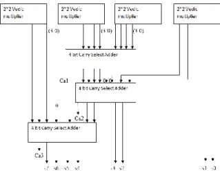
Vedic Multiplication for 8*8 bit module:
The equations are as follows: A=a7a6a5a4a3a2a1a0, B=b7b6b5b4b3b2b1b0
And the result will be 16bit length.
Fig. 4: Schematic diagram for 4*4 bit Vedic multiplier.
Proposed Technique:
In the proposed technique the ALU unit is designed with basic arithmetic and logical operations. Basic Arithmetic operations include addition, subtraction, multiplication and division and logical operations include logical and, logical or, logical nor, logical not etc. For designing the arithmetic operations unit resource sharing technique is used. In resource sharing technique the adders and other units are used for multiplication and subtraction operations. The units are designed in parallel which implies maximum utilization of the units and parallel processing advantage. The addition operation is performed using the fastest adder available in the literature with improved architecture. Carry Select Adder is for the realization of adder unit. In this , the ripple carry adder architecture (RCA) is used which computes the operation on the bits according to the fixed input taken as ‘1’ and ‘0’ and then the output is selected from these units using the multiplexer architecture with select line being the carry input value. The above architecture is improved by reducing the redundant resources and thereby reducing the area and timing complexity compared to the conventional RCA approach. Figure 5 shows the carry select adder design.
Fig. 5: Proposed Carry Select Adder design.
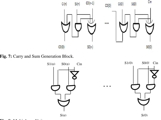
the main architecture of the adder is divided into different blocks comprising of half adder unit, carry and sum generation unit for ‘0’ and ‘1’ and the multiplexer block. In figure 6 half adder block architecture is shown and in figures 7 carry and sum generation unit is shown and in 8 multiplexing unit architecture is shown.
Fig. 6: Half Adder Block.
…
a(0) b(0)
a(n) a(n)
Ci(n )
Si(n )
Ci(0 )
Fig. 7: Carry and Sum Generation Block.
Fig. 8: Multiplexer Unit.
Using the proposed way of Carry Select Adder, addition unit of the proposed ALU is designed. The subtraction operation of the ALU is performed by taking the 2’s complement of the negative operand and then adding the operands using the addition unit. The multiplication unit is designed using the Vedic multiplier approach. 32 bit multiplier is implemented in the proposed ALU design which is in a hierarchical behavior with 32 bit multiplier is implemented using the 16 bit multiplier, 16 bit using 8 bit multiplier and so on. The division unit for the architecture is implemented using the finite state machine design approach which utilizes the concept of resource sharing by using the resources of adder.
RESULTS AND DISCUSSION
The proposed methodology is implemented using the Xilinx Spartan 6 FPGA and Verilog Hardware Description Language. The proposed technique is then compared with the basic approach on the basis of various performance parameters like number of slices and end to end delay. Table 1 shows the comparison of the resources used by the proposed and the basic approach.
Fig. 9: RTL of Vedic multiplier
…
S1(n) S0(n) Cin S1(0) S0(0) Cin
Table 1: Comparison Table
Fig. 10: Simulation waveforms of ALU.
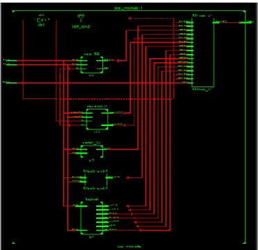
Fig. 11: RTL of proposed ALU.
Conclusion:
Bhandari, Nikhil and Shubhajit Roy Chowdhury, 2014. FPGA based High Performance Asynchronous ALU based on Modified 4 Phase Handshaking Protocol with Tapered Buffers. International conference on Devices, Circuits and Communications (icdccom), pp: 1-6.
Garima Rawat, Khyati Rathore, Siddharth Goyal, Shefali Kala., 2015. Design and Analysis of ALU: Vedic Mathematics Approach. International Conference on Computing, Communication and Automation, pp: 1372-376.
Jana Biswabandhu, Anindya Jana, Subhramita Basak, Jamuna Kanta Sing, and Subir Kumar Sarkar, 2015. Design and performance analysis of reversible logic based ALU using hybrid single electron transistor. Recent Advances in Engineering and Computational Sciences (RAECS), pp: 1-4.
Nautiyal, Priyanka, Pitchaiah Madduri, and Sonam Negi, 2015. Implementation of an ALU using modified carry select adder for low power and area-efficient applications. International conference on Computer and Computational Sciences (ICCCS), pp: 22-25.
Pandey, Bishwajeet, Jyotsana Yadav, Yatendra Kumar Singh, Ravindra Kumar, and Surabhi Patel, 2013. Energy efficient design and implementation of ALU on 40nm FPGA. In Energy Efficient Technologies for Sustainability (ICEETS), pp: 45-50.
Poornima, M., Shivaraj Kumar Patil, Shivukumar, K.P. Shridhar, H. Sanjay, 2013. Implementation of multiplier using vedic algorithm. International Journal of Innovative Technology and Exploring Engineering, 2(6).
Praveen, B., B.G. Tilak, S.B. Rashmi, 2011. An Optimised Design of 4-Bit Reversible Magnitude Comparator and Binary Subtractor. Published by Elsevier Ltd, GCSE.
Ramkumar, B. and H.M. Kittur, 2012. Low-power and area efficient carry select adder. In IEEE Trans. Very Large Scale Integration (VLSI) Syst, 20(2): 371-375.
Ravi Kishore Kodali, Lakshmi Boppana and Sai Sourabh Yenamachintala., 2014. FPGA Implementation of Vedic Floating Point Multiplier. Conference on Advanced technologies, pp: 1-4.