Other uses, including reproduction and distribution, or selling or
licensing copies, or posting to personal, institutional or third party
websites are prohibited.
In most cases authors are permitted to post their version of the
article (e.g. in Word or Tex form) to their personal website or
institutional repository. Authors requiring further information
regarding Elsevier’s archiving and manuscript policies are
encouraged to visit:
HBM tester waveforms, equivalent circuits, and socket capacitance
q
Timothy J. Maloney
⇑Intel Corporation, 2200 Mission College Blvd., SC9-09, Santa Clara, CA 95054, USA
a r t i c l e
i n f o
Article history:
Received 15 June 2011 Accepted 18 April 2012 Available online 20 May 2012
a b s t r a c t
The Tektronix CT2 current probe is used to acquire more accurate Human Body Model waveforms with 0Xand 500Xtester loads than a CT1, owing to the CT2’s low-frequency performance. The integrals and centroids of these waveforms then readily yield precise values of tester circuit elements and effective socket capacitance. Expressions are derived for effective socket capacitance resulting from distributed capacitance along a transmission line connecting to an unmatched load. These lead to options for reduc-ing the effective socket capacitance while retainreduc-ing the lines for deliverreduc-ing the HBM pulse.
Ó2012 Elsevier Ltd. All rights reserved.
1. Introduction
It was shown in 2009[1]that HBM waveforms taken with a 0-X
standard test load using a current probe can yield basic circuit modeling values for the tester, such as the charging capacitance Chb, the time constantRhbChb, and thus the series resistance Rhb.
These parameters are extracted from ‘‘moments’’ of the waveform (integral and centroid, or 0th and 1st moments in this case) as de-scribed in[1], and extend from circuit analysis dating back to the Elmore theorem[2]. While obtainingChbfrom integrated current
was fairly obvious, it was the Elmore theorem applied to the 2-pole RLC model of HBM that showed the ease of extracting trueRhbChb,
irrespective of inductanceL1. While Ref.[1]cautioned that current
measurements extracted with a CT1 current probe may have to be corrected for low frequency response of the probe, it is now found that the CT2 probe (also from Tektronix, Inc.) can provide good data for HBM tester characterization and circuit modeling, without significant need for correction.
The analytical methods of[1]can now be extended to a 4-pole model as used heavily for HBM work in the 1990s[3,4], to obtain circuit modeling information quickly and simply. As in[3], stan-dard waveform measurements with loads of 0 and 500Xare used to deduce values of the parameters, notablyChb,Rhb and socket
capacitance C2. Chb and Rhb are the basic Human Body Model
parameters, of course, while socket capacitance needs to be limited because it produces extra stress on many ESD protection devices, stress that could be inappropriately destructive. This was well rec-ognized in the 1990s and[3]presented electrothermal simulations showing the extent of that extra stress. Also, if a no-connect (NC) pin is stressed, the air will break down starting at about 800 V
and discharge the entire socket capacitance immediately, usually to a neighboring pin, producing an event far more destructive than HBM at the same voltage[5]. Ref.[3]also showed how difficult it was to achieve ‘‘selectivity’’ against high values ofC2using only
rise time and peak current standards with 0 and 500X. To deter-mine C2 accurately seemed to require computer-driven
multi-parameter analysis and curve fitting. In this work, we find thatC2
is far more accessible than we thought, through analysis of wave-form moments. Highly ‘‘selective’’ methods for finding equivalent C2could be adopted if we wish, or at least we could quickly
deter-mine theC2of a tester that might produce a problem with a device
during HBM testing.
2. Analytical foundations
2.1. Extraction of s-domain functions
The 2009 TLP and HBM waveform analysis work[1]discussed step response and continued with the insight of Elmore[2]and more recent authors[6,7], whereby it is shown that a waveform h(t) is transformed into the Laplace domain by expanding the exponent in the transform as follows:
HðsÞ ¼ Z 1
0
hðtÞestdt¼Z 1
0
hðtÞ 1stþs 2t2
2
s3t3
6 þ
dt
¼X
1
k¼0 ð1Þk
k! s kZ
1
0
tkhðtÞdt: ð1Þ
The various terms in the series are moments of the waveform, which yield coefficients of a Laplace domain functionH(s) =a0+
a1s+a2s2+ While an acceptable way of determining those
coefficients, given a digital oscilloscope waveformh(t), would be to do the time integrals as in(1)(and discussed in[1]in terms of
0026-2714/$ - see front matterÓ2012 Elsevier Ltd. All rights reserved.
http://dx.doi.org/10.1016/j.microrel.2012.04.009
q
This paper is co-copyrighted by Intel Corporation and the ESD Association. ⇑ Tel.: +1 408 765 9389.
E-mail address:[email protected]
Contents lists available atSciVerse ScienceDirect
Microelectronics Reliability
integration by parts), the Laplace transform formulation itself of-fers a more efficient and more easily implemented algorithm that was briefly treated in[1].
In this work,h(t) will be some kind of HBM waveform. Eq. (1) tells us that thea0coefficient ofH(s) is simply the integralh(t) from
start to finish. But the Laplace treatment also tells us that this integral function h1ðtÞ ¼R0thð
s
Þds
transforms to H1(s) =H(s)/s=a0/s+a1+a2s+ , as 1/sis the integration operator in the Laplace
domain. Essentially,h1(t) is a step of heighta0with other features
given by the rest of the coefficients. The Elmore Delay is indicated bya1, after normalizing toa0and accounting for the (1) factor.
The next time-dependent function of interest thus subtracts the basic step heighta0fromh1(t), i.e.,h01ðtÞ ¼
Rt
0hð
s
Þds
a0for whichthe transform isH0
1ðsÞ ¼a1þa2sþa3s2þ We are back where we
started withH(s), and know to finda1by integratingh01ðtÞto get
h2(t), then noting the step height again. The integral this time is
the ‘‘area capture’’ integral as shown in[1], Fig. 9 and also later in this work, Fig. 6. Because we subtracted the step height to form h01ðtÞ, the integral is, strictly speaking, negative in our example, but
that is expected from the (1) factor for that term in Eq.(1), given a positive waveform. Thus the Elmore Delay (a1/a0) is positive, as
expected. With digital data and integration with (for example) a spreadsheet program, we can determine any and all coefficients through iteration as above. For many waveforms therefore, partic-ularly a smooth one like HBM, the s-domain functionH(s) is thus available, rather easily, to a number of coefficients (limited only by noise) and can be related to circuit models that predict those coefficients.
The above algorithm is very time-efficient on the computer if one is interested in a low-order polynomial, i.e., just the first few s-coefficients for acquiring circuit element knowledge. ForNdigital points in the scope waveform, the integral for each coefficient is of orderNin time complexity, so forqcoefficients, there are on the order of Nq operations (O(Nq)). In this work, we will find that q= 2 applied to each waveform will be enough to determine our circuit elements. In contrast, using a fast Fourier transform (FFT) algorithm would have O(Nlog2N) time complexity and would
give N/2 frequency components, but this is far more information than needed for circuit modeling. The zero-frequency FFT compo-nent would correspond to a0 but we would still have to take a
derivative near zero frequency to finda1. Even so, given that
mod-ern digital oscilloscopes usually offer quick FFT conversion of a waveform to the frequency domain, one may well want to use that FFT function to extracta0anda1(or more coefficients) quickly with
a user-defined math function on the scope.
2.2. Transformers and their transfer functions
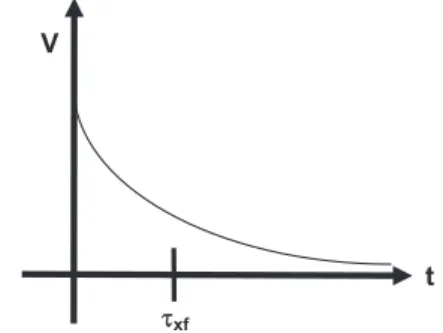
Another aspect of the 2009 work [1]that we will use is the notion of a transfer function for transformers, such as the CT1 and CT2 current transformers for HBM that this paper discusses. As shown in [1], the low frequency cutoff of the transformer is an important property because it describes the ‘‘droop’’ experi-enced as the transformer tries to follow the HBM waveform out into the decay time of 150 ns and beyond. To a remarkable degree, for a given current level the step response of one of these transformers is an exponential decay, as inFig. 1, so a single pole can describe the transfer function for that aspect. Another pole can describe high frequency rolloff, in which case the complete transfer function for a current transformer like the CT1 or CT2 can be approximated, ignoring normalization factors, by:
TðsÞ ¼ s
ðsþaÞðsþbÞ; ð2Þ
wherea= 1/sxf, as inFig. 1and Ref.[1], andb= 1/shf, indicating high
frequency cutoff. Note that all transformers have a zero at zero
fre-quency, thus thesin the numerator, but with that property, the step response is an easily observed exponential. As long as the frequency bis high enough to follow the rising edge of an HBM pulse well enough, our attention will focus on the a frequency or
s
xf.s
xf iscurrent-dependent for both CT1 and CT2 probes, but while it is around 6.35
l
s for the CT1, it can be well over 100l
s for the CT2. That will be significant.With two poles, the step response of the transformer is a double exponential, with a fast rise time. The impulse response of the transformer is, as usual, the derivative of the step response, and it is the impulse response that gives us, through convolution[8], the observed HBM waveform. The near-delta function in the cur-rent probe’s impulse response neart= 0 will faithfully reproduce the HBM waveform, but it is the negative slope of the step response that gives us a weak or strong negative multiplier for the real HBM waveform in convolution. That is why a long
s
xf is desired forfidelity.
3. HBM waveform measurement
The Tektronix CT1 current probe[9]has traditionally been used for HBM waveform characterization[3]. Its high-frequency cutoff, approaching 1 GHz, is excellent for HBM rise times and peak cur-rents, but its low-frequency cutoff is upwards of 100 kHz (Fig. 2a) and causes noticeable sag in step response even at the 1
l
s level[1]. Impulse response therefore has a strong negative component (imagine differentiatingFig. 1), and convolving such a response with the actual current waveform means that the decaying HBM current tail is depressed, and eventually drops be-low zero noticeably. This has surely caused systematic error in most measurements of HBM decay constant. Data taken with a CT1 can be corrected [1], but distortions are current-dependent[9], so it can be difficult to correct data accurately.
The Tektronix CT2 probe[9]has been found to be more suitable for HBM waveform measurement. Low-frequency cutoff is in the 1–10 kHz range (Fig. 2b), which much better fits the HBM decay time of 150 ns. Corrections are therefore negligible, and within electrical noise limits. This is indicated inFig. 3, comparing a sec-tion of the decay tail for the CT1 and CT2 probes on the very same pulse. The plunge below zero is clearly seen for the CT1. Mean-while, rise time curves and peak current for 0 and 500Xloads are almost indistinguishable for CT2 versus CT1. In this case of a Thermo MK-4 tester, there was less than 1% difference for those features, with 6–7 ns rise time for a 0Xload. The CT1 probe can always be used for rise time or peak current if there are any doubts about the CT2, but manufacturer data[9]indicates the impact of the CT2 bandwidth on those parameters may be negligible. At the same time, numerous measurements of the decay constant with the CT1 have shown that its droop, caused by low frequency response, is responsible for 0-Xload decay constants failing the 130 ns minimum spec[11], particularly at 4 kV, where distortion
V
t
τ
xfis greater. The CT2 then shows this ‘‘failure’’ to be a CT1 measure-ment artifact and not a tester fault. Use of the CT2 as the primary current probe for HBM waveforms is thus recommended.
4. 4-pole HBM model and circuit parameter extraction
The traditional four-pole model (also called 4th order model) of HBM is shown inFig. 4, with elements labeled as in[3]. One slight but important difference is the added voltage source, pictured as a step because we are indeed taking the circuit from chargedChbto
zero volts. We therefore are interested in the total admittance and response to a voltage step, giving the current.
Approximate values of the circuit elements are as follows:
Rhb¼1500
X
; Chb¼100 pF; C12 pF; L110l
H; R1¼0 or 500
X
; C220—50 pFIt has long been recognized[3,4]thatC2is the result of
distrib-utedcapacitance, and therefore will depend on howR1compares to
the effectiveZof the transmission line. Ref.[3]found that 500X
was high enough to reveal nearly all ofC2. We discuss more about
distributed capacitance in the next section.
The admittance functions for the circuit inFig. 4can be written with standard methods in the Laplace domain, and reduced to expressions for the currents we can measure with a current probe in series withR1, resembling some of the work done in[1]. The full
admittance function in the s-domain for the 4-pole network is:
YðsÞ ¼ Chbs
L1Chbs2þ1þRhbChbRhbC1ssþ
R1Chb 1þR1C2ssþ1
: ð3Þ
The step voltage isV=V0/s. For 0X,C2drops out, the network is
3rd order, and we measure the full current as:
I0ðsÞ ¼
V0Chbð1þRhbC1sÞ
1þb10sþb20s2þb30s3
; ð4Þ
whereb10=Rhb(Chb+C1),b20=L1Chb,b30=L1ChbRhbC1.
Full current is hard to measure for nonzeroR1, and is treated in Appendix A. ForR1= 500X, the current in the 500Xbranch is:
I500ðsÞ ¼
V0Chbð1þRhbC1sÞ
1þb1500sþb2500s2þb3500s3þb4500s4
; ð5Þ
where b1500=Rhb(Chb+C1)+R1(Chb+C2), b2500=RhbR1(Chb(C2+
C1)+C2C1)+L1Chb, b3500=L1Chb(RhbC1+R1C2), and b4500=L1Chb
(RhbC1R1C2). In both cases the 0th order response is the total charge,
Qt=V0Chb. Fig. 5 shows 0 and 500X test load waveforms for a
Thermo MK-4 tester with a CT2 probe, both revealing a capacitance Chbof about 114 pF.
Fig. 2b.Tektronix CT2 probe data, from[9].
CT2 and CT1, 500 ohm
-0.01 -0.005 0 0.005 0.01 0.015 0.02 0.025 0.03
760 780 800 820 840 860 880 900 920
time, nsec
current, A
CT1 CT2
Fig. 3.Expanded view of 500XHBM tails for CT1 (lower) and CT2 (upper) current probes, with CT1 signal going negative because of its low frequency cutoff.
C1
Chb
Rhb
L1
C2 R1
V0
Fig. 4.Fourth order model of HBM ESD tester, including parasitic capacitances and inductance. As Chb is initially charged to ±V0 and then discharges, HBM is conceptually the step response of this network.
Things get interesting as we investigate centroids of these wave-forms, following the methods in[1]and as described in Section2
above. In particular, Ref.[1]and Section2proved that the areaA above the integrated current curve, divided byQt, gives the centroid
of the original waveform (units of time), as shown inFig. 6. The centroids
s
0 ands
500 are of course the first-order s-coefficients(times -1) of the series expansions of the current expressions(4) and (5), again following[1]:
s
0¼b10RhbC1¼RhbðChbþC1Þ RhbC1¼RhbChbs
500¼b1500RhbC1¼RhbðChbþC1Þ þR1ðChbþC2Þ RhbC1 ¼RhbChbþR1ðChbþC2Þ:
ð6Þ
Note that
s
0is unchanged from the simple 2-pole model in[1].In(5), letR1be the true value of the 500Xresistor,R500. The socket
capacitanceC2therefore is:
C2¼
s
500s
0R500
Chb ð7Þ
Note thatC1andL1have dropped out of the analysis and appear
only in higher order moments. For the MK-4 tester discussed above, the complete set of extracted values is listed in Table 1. The socket capacitanceC2= 13.9 pF is considered a very good
re-sult, and indeed the waveforms easily passed all specs related to socket capacitance.
At the same time, older Zapmaster HBM testers, configured for 512 and 256 pins, at two different Intel sites, gaveRhbandChb
val-ues as shown (see Table 1), but with higher socket capacitance C2= 47–51 pF. Sure enough, in the 512 case the 500XIpeak value
did not pass spec. The 0-Xload decay for the 512 was short enough that it failed on a CT1 probe (128 ns) but passed on a CT2 (135 ns). The 256 waveforms narrowly passed specs on the CT1 but had much healthier margins on the CT2. All this is in agreement with the notion that JEDEC and ESDA HBM specs were formulated with
the intention of tolerating up to 50 pF of equivalent socket capacitance.
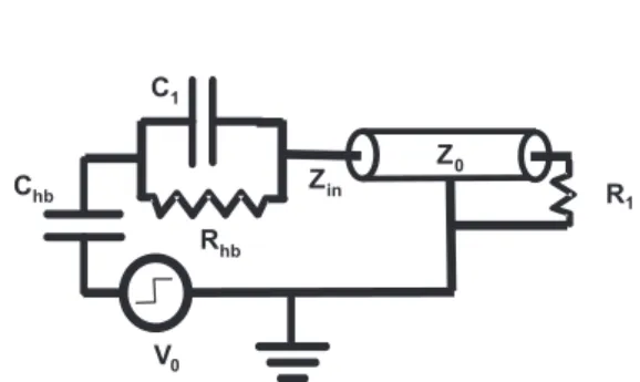
5. Distributed socket capacitance
An automated HBM ESD tester acquires much of its apparent inductanceL1and socket capacitanceC2from the distributed
trans-mission lines through the relays to the socket board. That portion of the lumped element model as inFig. 4can be found from a first order approximation of the transmission line model, terminated by resistanceR1(0 and 500X) with line impedanceZ0= 1/Y0. This is
illustrated inFig. 7, for which we want to find a simple network equivalent of ZinorYin. ForR1= 0, there will be someL1 and no
C2, but from Eqs. (1)–(7), it is clear that L1 does not affect the
first-orderC2calculation that we arrive at in Eq.(7)once we have
a lumped model. Thus we turn to the case ofR1= 500Xand look at
the input admittance, aiming for Ym¼R1
1þj
x
Cx¼Y1þsCx and effective capacitanceCx. From transmission line theory[10]:Yin¼Y0
Y1þY0tanh
c
l Y0þY1tanhc
l
Y1þsY0 ffiffiffiffiffiffi
LC p
l
1þsY0
Y1
ffiffiffiffiffiffi
LC p
l ð8Þ
for low values of
c
‘,c
the propagation constantjx
pLCffiffiffiffiffiffi¼spffiffiffiffiffiffiLC,L andCthe capacitance and inductance of the line per unit length, and‘ the line length. AlsoY20¼C=Lfor the lossless transmissionline. To first order, the denominator expands for low values of
c
‘to multiply the numerator, resulting in:
Yin¼Y1þs Y2
0Y
2 1 Y0
ffiffiffiffiffiffi
LC p
lþ : ð9Þ
If the full distributed capacitance isC2=C‘, this becomes:
Yin
1
R1
þsC2 1 Z2
0 R21 !
¼1 R1
þs
a
C2: ð10ÞAs expected, the effective capacitance Cx=
a
C2 declines withhigherZ0and tunes out completely with an impedance match of
R1=Z0. This means that one strategy for reducing Cx is to raise
the effectiveZ0, say by distributing nearly lossless ‘‘loading coils’’
(e.g., ferrite beads) along the line. This recalls a coil loading method used in the 19th century to reduce the resistive attenuation of tele-graph signals, as the attenuation length is approximately 2Z0/R, R
the resistance per unit length[10], although the purpose here is Fig. 5.0 and 500Xtest load waveforms, 1 kV, CT2 probe, measuringQt= 114 nC in
each case for an MK-4 tester.
Fig. 6.Integrated current for a 1 kV HBM waveform, converging to total chargeQt. The centroidsof the original waveform is computed fromA/Qt=s, whereAis the area above the curve, and is the Elmore delay of this integrated current curve. Related theorems are proven in[1].
Table 1
Major circuit model values and time constants for three different HBM testers at two different sites, using CT2 probe and 0 and 500X(R500= 500–501X) loads.
Tester Chb(pF) Rhb(kX) s0(ns) s500(ns) C2(pF)
MK-4 114 1.412 161 225 13.9
Zapmaster 512 101 1.445 146 222 51 Zapmaster 256 113.4 1.340 152 232.5 47.3
C1
Chb
Rhb
Z0
R1
V0
Zin
slightly different. The extra total inductance puts some limits on the shortest achievable HBM rise time (seeAppendix A), but the 2–10 ns window for 0-Xloads[11], for example, should not be threatened by a few extra microhenries.
Another way to reduceCxis to borrow from the HBM network’s
1500Xof series resistance and distribute some resistanceRaalong
the transmission lines that also have their distributed capacitance
totaling C2. If the inductance now becomes negligible,
c
l¼ ffiffiffiffiffiffiffiffiffiffiffiffiRaC2sp
; Z0¼
ffiffiffiffiffiffiffiffi
Ra sC2;
q
and:
Zin¼Z0
1þZ0
R1tanh
c
‘Z0
R1þtanh
c
‘" #
¼Z0tanh
c
‘1þZ0tanhc‘ R1
Z0tanhc‘
R1 þtanh 2
c
‘ 24
3
5: ð11Þ
But for small
c
‘, tanhc
‘c
‘,Z0c
‘=Ra, and:ZinRa
1þRa R1
Ra R1þsRaC2
" # ¼ 1þ
Ra R1 1
R1þsC2
: ð12Þ
This means that:
Yin
1
R1þRa
þs
a
C2; ð13Þwhere
a
=R1/(Ra+R1), and corresponds to the circuit model in Fig. 8. The effective capacitanceCx=a
C2and is reduced accordinglyby the distributed resistanceRa. But if the total inductanceLtis not
negligible,Rais simply replaced byRa+sLt(=Z0
c
‘) in (12) and (13),leading us to a more general expression:
Yin¼
1
R1þ sC2
R
1 RaþR1
1
1þZ002C2s
RaþR1
0 @ 1 A 2 4 3
5: ð14Þ
We now takeZ0
0¼
ffiffiffiffi
Lt C2
q
for the transmission line, while the ac-tual impedance is complex and includes the effect ofRa. Expanding
this to first order, we have:
Yin
1
R1þRa
þsC2 R1 RaþR1
1 z
02 0 R1ðRaþR1Þ
: ð15Þ
This reduces to(10)forRa= 0 and to(13)forLtorZ00negligible,
so now we see that the general capacitance reduction factor is:
a
¼ R1 RaþR11 Z
02 0 R1ðRaþR1Þ
!
ð16Þ
for a transmission line with inductive and resistive loading as above. From this expression, it can be easily shown that the tradeoff ofRaandZ00is particularly simple when
a
< 0.5 is desired, as thatcondition is:
R2
aþ2Z
02 0 >R
2
1: ð17Þ
Therefore whenR1= 500X,
a
< 0.5 is achieved with 300Xforeach ofRaandZ00, for example, along with other solutions beyond
the elliptical boundary in theRaZ00plane. Lower effective
capac-itance of this kind also has the desired effect on sudden destructive currents that can be delivered in snapback[3]or in breakdown of a no-connect pulse[5], as the inductive and resistive loading limits the current.
6. Conclusions
The Tektronix CT2 current probe is found to be adequate for short-time HBM waveform measurements like rise time and peak current, and more suitable than the same manufacturer’s CT1 probe for long-time measurements like decay constant. CT2 wave-forms do not suffer from significant droop in HBM waveform tails, making them suitable for circuit element extraction through asymptotic waveform analysis methods, even with a 4-pole model of HBM.
Integration of the 0-Xload waveform gives main HBM capaci-tanceChb, and the waveform’s first moment or centroid gives the
RhbChbtime constant
s
0and thereforeRhb, through straightforwardand essentially graphical means. While the authors of Ref. [3]
found that only a careful multi-parameter fit to waveforms could determine a best value ofC2, the methods here, summarized by
Eq.(7), allow tester equivalent socket capacitanceC2to be
accu-rately measured from the 0-Xvalues (Chb,
s
0) plus the 500Xcen-troid time constant. This allows a precise measurement of this important value with a simple, easily accessible method, as the er-ror inC2should be limited only by noise and numerical accuracy.
The method leading up to Eq.(7)provides the ‘‘selectivity’’ forC2
that has long been sought by ESD researchers. A related qualifica-tion standard would depend on acceptance of digital waveform re-cords and procedures for extracting simple integrals and centroids from the waveforms.
Much of the effective socket capacitance
a
C2in an HBM testercan result from the necessarily long distribution lines from the HBM network module to the component at the socket. The net-work analysis methods of this paper are extended to find the effec-tive socket capacitance that results from (1) the known finite impedance and terminating load of the transmission line, and (2) distributing some of the required 1500X of series resistance throughout this transmission line. Simple general expressions for
a
C2 then show how inductive loading and/or distributed seriesresistance can substantially reduce this capacitance and thus reduce unwanted extra stress during the HBM test. Newer HBM testers have much lower
a
C2and are already using these methods.Acknowledgments
The author would like to thank Russell Sears, Marti Farris and Abishai Daniel of Intel for the HBM tester data, acquired using both CT1 and CT2 current probes. Thanks also to Evan Grund for manuscript review and additional insights.
C2
Z0, Ra
Yin R1
R1 Ra
Appendix A. additional mathematics
For nonzeroR1, the full current is found from Eq.(3)to be
Ifull500ðsÞ ¼
V0Chbð1þRhbC1sÞð1þR1C2sÞ
1þb1500sþb2500s2þb3500s3þb4500s4
: ðA1Þ
This is Eq.(5)with one more zero. Thus the measuredI500(t) is
the convolution ofIfull500(t) with exp(t/R1C2), so for a fast rise
time onIfull500(t), theR1C2time constant is expected to add to it
and dominate the rise time ofI500(t). HBM test standards[11]have
agreed with this.
Note that all these network functions are ratios of polynomials. The essential properties of the functions can be examined by con-sidering each network function to be:
HðsÞ ¼ 1þa1sþa2s
2þ þa
nsn
1þb1sþb2s2þ þbmsm ð
A2Þ
mPn, and corresponding to time domain functionh(t). It is useful to expandH(s) abouts= 0 to obtain an infinite series in powers ofs:
HðsÞ ¼1þ ða1b1Þsþ ða2b2b1a1þb 2 1Þs
2
þ ða3b3
a1b2þ2b1b2a2b1þa1b 2
1b
3 1Þs
3þ : ðA3Þ
This kind of result appears in many works on signal integrity
[6]. It is also useful to consider the factors of the numerator and denominator ofH(s), described by thempolespiand thenzeros
zithat form the roots of the polynomials. It is a consequence of
Vieta’s Formulas describing the relations among symmetric poly-nomialsSq[12]of these roots to the coefficients that we can form
Sn1/Snfor the poles and zeros and find that:
Xm
i¼1
1
pi
¼ b1; Xn
i¼1
1
zi
¼ a1: ðA4Þ
Remember that the real parts of our poles and zeros will typi-cally be negative numbers, and the coefficients positive real, so the minus signs can be dropped if we regard the reciprocal poles and zeros as positive time constants. Note also that complex con-jugate poles or zeros
r
±jx
add together to become a real number 2r/(r2+x
2).The fact that the poles and zeros sum to an easily calculated number can be used to refine some of our estimates. In the 1993 work by Verhaege et al. [3], the main decay constant
s
2 for the4th order network is found to be:
s
2¼ ðRhbþR1ÞðChbþC1Þ: ðA5ÞFor the shorting waveformR1= 0, this reduces to:
s
20¼RhbðChbþC1Þ: ðA6ÞHowever, in the expression forI0(s), Eq.(4), this corresponds to
b10, the sum of all the poles, including rise time plus decay
con-stant. It is clearly correct forL1= 0, where everything collapses to
a single pole, but then the rise time would be zero and out of spec. Some influence of inductance is expected, as is the case for a 2-pole network (note that 1/a+ 1/b=RhbChb). By starting withL1=R1= 0
and adding inL1as a ‘‘small’’ perturbation, one gets:
s
20RhbðChbþC1Þ L1 Rhb12C1 Chbþ
L1Chb
R2
hbðChbþC1Þ 2
!
: ðA7Þ
The last term indicates the rise time of the HBM network, with the expectedL/Rleading term.
References
[1] Timothy J. Maloney. Evaluating TLP transients and HBM waveforms.In: EOS/ ESD symposium proceedings; 2009, p. 143–51.
[2] Elmore WC. The transient analysis of damped linear networks with particular regard to wideband amplifiers. J Appl Phys 1948;19(1):55–63.
[3] Verhaege K, Roussel P, Groeseneken G, Maes H, Gieser H, Russ C, et al. Analysis of HBM ESD testers and specifications using a 4th order lumped element model. In: EOS/ESD symposium proceedings; 1993, p. 129–37.
[4] van Roozendaal L, Amerasekera A, Bos P, Baelde W, Bontekoe F, Kersten P, et al. Standard ESD testing of integrated circuits.In: EOS/ESD symposium proceedings; 1990, p. 119–130.
[5] Kunz H, Duvvury C, Brodsky J, Chakraborty P, Jahanzeb A, Marum S, et al. HBM stress of no-connect IC pins and subsequent arc-over events that lead to human–metal-discharge-like events into unstressed neighbor pins.In: EOS/ ESD symposium proceedings; 2006, p. 24–31.
[6] Gupta R, Tutuianu B, Pileggi LT. The Elmore delay as a bound for RC trees with generalized input signals. IEEE Trans Comput-Aided Des Integr Circ Syst 1997;16(1):95–104.
[7] Celik M, Pileggi L, Odabasioglu A. IC interconnect analysis. New York: Kluwer Academic Publishers; 2002.
[8] Bracewell RN. The Fourier transform and ıts applications. New York: McGraw-Hill; 1965.
[9] Web article, Tektronix page on CT1, CT2, and CT6 current probes. <http:// www.2.tek.com/cmswpt/psdetails.lotr?ct=PS&lc=EN&ci=13500&cs=psu.> Figs. 2a, 2b used with permission.
[10] Ramo S, Whinnery J, Van Duzer T. Fields and waves in communication electronics. New York: John Wiley & Sons; 1965. p. 46.
[11] ANSI/ESDA/JEDEC JS-001-2010, ESDA/JEDEC joint standard for electrostatic discharge sensitivity testing–human body model (HBM)–component level (Jan. 2010 <www.jedec.org> and <www.esda.org>.
![Fig. 2b. Tektronix CT2 probe data, from [9].](https://thumb-us.123doks.com/thumbv2/123dok_us/8195500.2172630/4.892.66.409.138.473/fig-b-tektronix-ct-probe-data-from.webp)