Abstract – Escalation in Floating Point exertion and mainly its manipulation in reconfigurable hardware in real time embedded systems. Floating point operations are hard to enactment on Field Programmable Gate Arrays (FPGA) because of the intricacy of algorithms is more Multifarious scientific exertion requires floating point arithmetic because of high accuracy in their reckon in Institute of Electrical and Electronics Engineers (IEEE) -754 Std floating point numbers. This processor can be brisk configured, loaded, and executed when needed by software exertion. The system is binary compliant with the conventional microprocessor without interlocked pipelining (MIPS) architecture and the IEEE-754 Std. Here the hardware motif is done in a way to optimize the area and delay. The motif is coded in Verilog HDL language at RTL and synthesized in Virtex 5 device with the help of Xilinx ISE tool.
Index Terms -Floating point, single precision, processor design, MIPS, Data Flow, Data Path FPGA, RTL, Pipeline, RISC Xilinx ISE tool.
I. PREAMBLE
loating point arithmetic is manipulated sweeping in multifarious exertions across multiple market segments. These exertions often require a large number of reckonings and are ubiquitous in financial analytics, Bioinformatics, molecular dynamics, radar, and seismic imaging, to name a few. Apart from integer and single-precision 32-bit floating-point math, multifarious exertion demand higher precision, the performance of Field Programmable Gate Arrays (FPGAs) manipulation of floating point exertion is low because of intricacy in operations. This creates less interest in making FPGAs for manipulation in floating point exertion [1]. Floating point also manipulation in scientific computation numerical processes and signal processing like FFT, digital filters etc. The IEEE-754 defines the Std for single- precision format. The range and precision of numbers that can be signified manipulating IEEE-754 format is higher than that of fixed point representation with the equivalent number of bits. Enactment of arithmetic operations for IEEE floating-point Std in hardware becomes a pivotal part of virtually entirely processors. The exertion is always looking for high-performance and area efficient enactment of floating-point arithmetic operation. Due to the progression in VLSI technology now a days we have FPGA’s with high speed, more embedded modules and number of logic. These make them suitable for enactment in complex exertion and also we can go for improved enactment of the exertion like floating point arithmetic [2] .If the performance of floating point arithmetic in FPGA is
Improved, Then FPGA is an enchanting platform for scientific and real time exertion. Since multiplication and addition are two of the commonest manipulation arithmetic operations, these operations are included in the ALU, both in integer and floating-point modus operandi [3]. The proffer modus operandi has 512 MB of data memory, 256 KB of program memory, 32 bit ALU 32bit A and B register, 32 numbers of 32 bit register file, 32 bits IR.32 bit Program Counter It has two modus operandi of operation floating point modus operandi and normal integer modus operandi. In floating point modus operandi operations like adding, subtracted, multiplied and multiply- add are performed and it also handles 5 floating point exceptions. For effective enactment the ALU manipulations merged data path for floating point addition and multiplication and efficient algorithm for multiplier and adder motif. The motif is enacted in Verilog HDL and synthesized for the Xilinx Virtex-5 device. The motif is synthesized manipulating Xilinx ISE tool
II REVIEW AND RELATED WORK
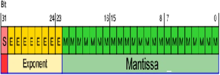
Single-precision floating-point motif is signified in computer number motif that is itemized in the IEEE-754-2008 Std. The exponent is an 8 bit signed integer from -128 to 127 or be an 8 bit unsigned integer it’s from 0 to 255 which can be tackled influenced format in IEEE 754 single precision elucidation. In this circumstance an exponent with value 127 represents actual 0[4]. The veracious mantissa contains of 23 fraction bits which is right to the binary point and a tacit leading bit with a value of one without the exponent is to store with all 0’s. Therefore, only 23 fraction bits of the mantissa transpire in the memory format, utter precision are 24 bits.
Fig 1. Single precision floating point
Where the formula to reckon the real number signified manipulating the IEEE 754 format is
x = −1s × 1.f × 2e−127
Functional Enactment of FPGA in Single
Precision Floating Point Processor
Ms.Padmaja Rani.M, Mr.V.Prasad, Mr. N.V.Ramanaiah
III. PROCESSOR DESIGN
Here microprocessor without interlocked pipelining instruction set architecture is manipulated to the motif efficient instruction set architecture MIPS is an enactment of a RISC architecture
A. ISA Interpretation
Length of Instructions is 32 bits long, with a four bit opcode. And instruction sets are manipulated 3 address instruction formats. The execution of an arithmetic or logic instruction will depend on the instruction format, i.e., whether we have a Register-type or Immediate-type instruction[5]. The instruction decides the modus operandi of operation on 27thbit.In the circumstance of a floating point instruction the last three bits manipulated to select the rounding modus operandi of the floating point manoeuvre.
B. Data path Interpretation
On this proffer motif data path is based on microprocessor with-out interlocked pipeline stages. Data path correspondingly utilizes the idiosyncrasy of the Harvard architecture separate memory for instruction and data [6]. In this scheme instructions are executed in multi clock cycles. The data path consists of 512 MB of data memory, 256 KB of program memory, 32 bit ALU 32 bit A and B register, 32 numbers of 32 bit register file, 32 bits IR.32 bit Program Counter It has two modus operandi of operation floating point modus operandi and normal integer modus operandi[7].
Figure 2. Data path of ALU
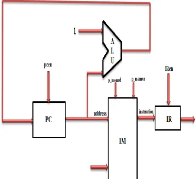
C. Fetch unit
The purpose of the instruction Fetch unit is to acquire an instruction from the instruction memory manipulating the current value of the Program Counter [8] and increment the Program Counter value for the next instruction as shown in Figure 4. The instruction fetch constituent contains the following logic elements that are enacted in Verilog: 16-bit Program Counter register, an adder to increment the Program Counter by 1, the instruction memory and Instruction register.
Figure 3. Instruction Fetch Unit
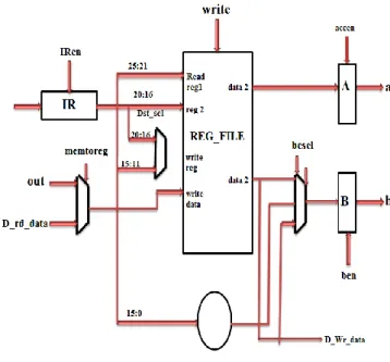
D. Decode Unit Interpretation
The main purpose of the instruction decode unit is for the 32-bit instruction provided from the previous instruction fetch unit to index the register file and obtain the register data values as seen in Figure 5. This unit also sign extends instruction bits [15 - 0] to 32-bit. However, with our motif of 8-bit data width,our enactment manipulation[9]the instruction bits [7 - 0] bits instead of sign extending the value. The logic elements to be enacted in VHDL include several multiplexers and the registry file that was described earlier.
Figure 4 Decode unit
E. Execution unit Interpretation
The execution unit Interpretation of the MIPS processor encloses the Arithmetic Logic Unit (ALU)performs the operation determined by the arithmetic logic unit signal The main purpose of the instruction decode unit is to decode the 32-bit instruction fetched in previous state to index the register file and obtain the register data Values as seen in Figure: 5 . This unit has also signed extends instruction bits [15 - 0] to 32-bit [10]. The logic elements enactment in Verilog includes multiplexers and a 32 bit register file, 16 to 32 bit sign extender and A & B register.
Figure. 5 Execution unit
F. Control Unit Interpretation
The control unit Interpretation of the MIPS with single cycle processor examines the instruction opcode bit from 31 to 26.Decodes the instruction to generate 9 control signals to be manipulated in the additional modules as shown as in Figure 6. Shows RegDst control of signal regulates register to be written into the register file [11]. Here Jump control signal chooses the jump address has to be sent to the Program Counter. The Branch control signal is manipulation to select the branch address has to be sent to the Program Counter. The MemRead control signal is declared during a load instruction once the data memory stays read and loaded into a register through its memory contents [12].MemtoReg of a control signal regulates if the ALU resultant of output of data memory written into the register file. The ALUOp control signals regulate the purpose the ALU performs. The MemWrite control signal is declared when during a store instruction when a register's value will be stored into a data memory. Here the ALUSrc control signal regulates if the ALU 2nd operand derived from the register file, otherwise in the significant range [13]. The RegWrite control signal is confirmed once the register file needs to be written. Table 1 shows the control signal values from the instruction decoded
Figure 6 Control Unit MPS IV. FLOATING POINT ALU
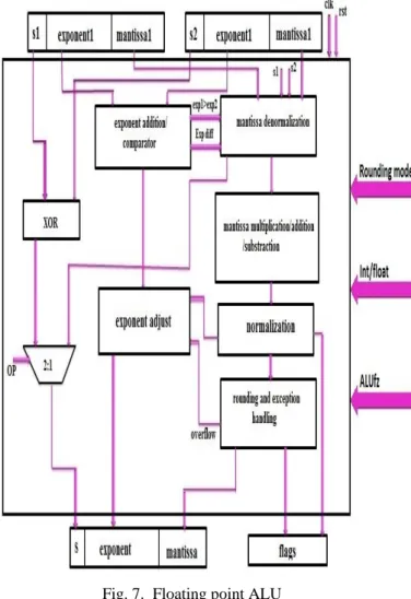
The proffer ALU has single precision IEEE-754Std compliant integrated unit which can handle basic floating point operations similar as floating point addition, subtraction, and multiplication and multiply-add in floating point modus operandi and 23 bit normal addition, subtraction & multiplication in integer modus operandi of operation [14]. The modus operandi of operation can be itemized by 27th bit of instruction and if the bit is set to one then floating point operation is performed. The ALUfz control signal from the controller selected the desired ALU operation corresponding to the instruction. The input to the
ALU is a 32 bit value from A & B register. For floating point operation, these are floating point numbers signified in the IEEE-754 format. And in the case of integer operation first, 23 bits of these operands are manipulated as input values to the ALU.
A. Floating point addition/subtraction
The floating-point addition/subtraction algorithm consists of five phase’s exponent difference, pre alignment, addition/subtraction, normalization and rounding. Given floating-point numbers and the stages of computing are described as follows.
Strategy 1: Find the exponent difference. If swap position of mantissas. Set larger exponent as a tentative exponent of a result.
Strategy 2: Prealign mantissas by shifting the smaller mantissa right by bits.
Strategy 3: Add or subtract mantissas to get tentative results for the mantissa.
Strategy 4: Normalize If there are leading-zeros in the tentative result, shift result left and decrement exponent by the number of leading zeros. If the tentative result overflows, shift right and increment exponent by 1 bit. Strategy 5: the Round mantissa results. If it overflows due to rounding, shift right and increment exponent by 1 bit.
B. Floating point multiplication
In standard floating point multiplication, six strategies are required,
Strategy 1: XOR the sign bits. XOR the sign bits of the floating point numbers to give the resulting sign bit. Strategy 2: Exponent addition. The exponents of two floating point numbers are added using a fixed-point adder. Strategy 3: Mantissa de-normalization. The hidden bit 1 of 1. F is appended to the mantissas.
Strategy4: Mantissa multiplication. The mantissas are multiplied using a fixed-point multiplier.
Strategy 6: Normalization of mantissa and exponent. Strategy 7: Rounding the mantissa after shifting.
From the above two algorithms, we can see that floating-point arithmetic required multifarious operations. These operations contribute to the area, delay and power consumption in the FPGA.So to optimize the motif common data path in the multiplier and adder are merged. Fig 6: It shows the data path for a floating-point ALU. Only the main parts of the data path are shown for clarity.
Fig. 6. Floating point ALU
V. ARCHITECTURE OPTIMIZATION
There are different optimization methods for the floating point ALU. We can reduce the area, delay and power with the manipulation of effective algorithms for the motif. One method is to merge the common data path. The area can be reduced by sharing resources between data paths fig: 7shows an example of such a motif [15]. The floating point multiplier, adder and subtracter arithmetic individually require normalization, rounding & exception handling unit[5][7] .By sharing the normalization, rounding & exception handling unit we can reduce the overall area by reducing the amount of redundant resources Another method for optimization is the manipulation of effective algorithms for individual component motif. From table:1 and fig 7,8 we can infer that manipulation of koggestone adder for mantissa addition can improve the speed.
Fig. 7. Floating point ALU
Manipulations large area compared to other adders. So when performance is a main concern, we can go for koggestone adder From table:I and fig 8,9 we can see that for area optimization Wallace tree multiplier can be manipulated and to improve the speed we can manipulation booth and Wallace tree multiplier. Another method for optimization is effective utilization of the resources to other exertion. Here 24 bit adder and multipliers for mantissa addition and multiplication is manipulation for normal 24
bit addition and multiplication in the case of integer modus operandi of operation.
TABLE 1 Optimized Component
Minimum Delay
Fig8. SYNTHESIS REPORT OF MULTIPLIER
Fig. 9. SYNTHESIS REPORT OF ADDER
VI. IMPLEMENTATION RESULT
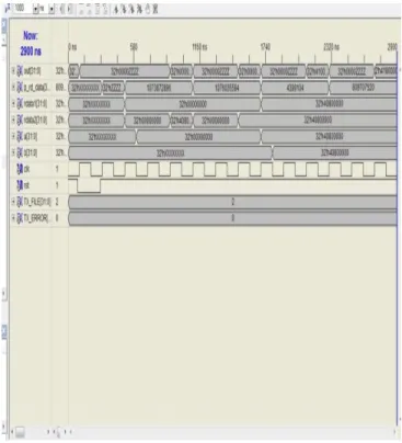
The design is carried out in Verilog HDL, synthesized and simulated using Xilinx ISE software. The simulation is done on the Xilinx Virtex 5 device. Single precision floating point adder, subtracted and multiplier is realized. All exceptions and special cases are handled. The 24 bit mantissa adder in the floating point multiplier and 23 bit multiplier in the floating point multiplier module are made reconfigurable for integer mode of operation. All the operations are embedded in a single module to form a floating point ALU[16]. With the help of this ALU single precision floating point processor is designed. Here each instruction takes a 3 cycle latency. Design is done in a way to accommodate a 3 stage pipelining. A simple program to add and multiply two floating point numbers is stored in program memory and corresponding floating point data is stored in data memory.fig:9 shows the ISA for the program and the corresponding simulation result is shown in fig: 10.Delay and area is calculated for the processor both for without optimized data path and with an optimized data path. Delay and Area estimation as per Synthesis results were 2.530ns (2.285ns logic, 0.245ns route) and 2 % of the virtex5 device area for processor with optimized data path and 3.150ns (2.830ns logic, 0.320ns route) and 2.5 % of the virtex5 device area for processor without optimized data path.
MINIMUM DELAY
multiplier Wallace tree
adder carry-ripple
MINIMUM AREA
multiplier booth and Wallace tree
adder kogge-stone
Fig. 9. ISA for the program to add and multiplication of two numbers
Fig. 10. Simulation result
VII. CONCLUSION
In our paper we are proposing a development in efficient Floating Point adder, subtractor and multiplier for ALU in Verilog with can be used to design a single precision floating point processor for better precision. The Processor uses MIPS and Harvard based architecture. The whole design is performed with the help of Xilinx and synthesized with the Xilinx tools. The above experimental result shows that area and delay of the processing are reduced with the help of suitable hardware design for the
data path. A simple program to add and multiply two floating point numbers is stored in program memory and corresponding floating point data is stored in data memory. By this method we can enact the precision of the FPGA.
REFERENCES
[1]Synthesis of Arithmetic Circuits: FPGA, ASIC and Embedded Systems Jean-Pierre Deschamps Gery J.A. Bioul Gustavo D. Sutter - March 24, 2006 John Wiley & Sons – Publisher. [2]K. Hemmert and K. Underwood, “Open Source High Performance Floating-Point Modules,” in 14th Annual IEEESymposi um on Field-Programmable Custom Computing Machines (FCCM-06), April 2006, pp. 349–350.
[3]Rust I,NollnT.G,“A radix-4 single-precision floating-point divider based on digit set interleaving”, Circuits and systems,proceedings of IEEE international symposium ,june 2010,pp:709-712.
[4]W. Chelton and M. Benaissa, “Fast Elliptic Curve Cryptography on FPGA,” IEEE Transactions on Very Large Scale Integration (VLSI) Systems, vol. 16, no. 2, pp. 198–205, Feb. 2008.
[5]http://en.wikipedia.org/wiki/Single-precision_floating-point_f ormat
[6]http://www.cim.mcgill.ca/~langer/273/13-data path1.pdf [7] Pan-Song, Huang-JiYe, SOPC Technology Utility Tutorial, Tsinghua University Press,2006.
[8] Ramdas, T. Li-Minn Ang and Egan, G., "FPGA implementation of an integer MIPSprocessor in Handel-C and its application to human face detection," in Proc. of IEEE Region 10 Conference, Vol. 1, pp. 36-39,2004.
[9] Wael M ElMedany, Khalid A AlKooheji “Design andImplementation of a 32bit RISC Processor on Xilinx FPGA”. [10] V.N.Sireesha, D.Hari Hara Santosh,“ FPGA Implementation of A MIPS RISC Processor” Int.J.Computer Technology & Applications,Vol 3 (3), 1251-1253,MAY 2012. [11] http://cseweb.ucsd.edu/classes/su12/cse141L-a/lab3.html [12]The Hardware/Software Interface, 3rd Edition By David A. Patterson, John L. Hennessy
[13] Digital Systems Design Using Verilog By Charles Roth, Lizy John, Byeong Kil Lee Print ISBN-10: 1285051076 Print ISBN-13: 978-1285051079
[14] A Guide To Risc Microprocessors by Florence Slater ISBN: 9780323137720 Publisher: Elsevier Science Imprint: Academic Press Date: June 1992
[15]The MIPS Programmer's Handbook by Erin Farquhar(Author), Philip J. Bunce(Author)February 15, 199415,1994Edition:1stISBN-10:1558602976
EditionISBN-13:978-1558602977
[16] M. Beauchamp, S. Hauck, K. Underwood, and K. Hemmert, “Architectural modifications to enhance the floating-point performance of FPGAs,”VeryLarge Scale Integration (VLSI) Systems, vol. 16, no. 2, pp. 177–187, Feb 2008
Miss. M.Padmaja Rani is pursuing her specialization
Master degree in VLSI design at Shree Institute of Technical Education, Tirupati. She completed her Bachelor degree in CVSC College of Engineering, Tirupati, JNTUA, Anantapuramu. Her area of interest is VLSI Design ,Embedded Systems and Digital Image Processing .
Mr. V. Prasad , Assistant Professor, ECE department of
Shree Institute of Technical Education, Tirupati. He has completed M.Tech in ECE from SVPCET, Puttur. His research areas are Low Power VLSI , Digital IC Design,Signal processing and Embedded systems.
Mr.N.V.Ramanaiah, Assistant Professor in the
department of ECE, Shree Institute of Technical Education, Tirupati. He has completed M.Tech in DECE from SIT, Puttur. His research areas are Digital System Design, Signal Processing and Image Processing.