Synchronous Fly Back Converter Implementation
Chittajit Sarkar
Swami Vivekananda Institute of Science and Technology, West Bengal University of Technology, Kolkata, India Email: [email protected]
Abstract—Purpose of this paper is to describe the hardware design implementation of synchronous fly back converter featuring the LT3825. This circuit was designed specifically to attain a high current, low ripple, synchronously rectified fly back to efficiently power 3.3V loads at up to 12A from a typical telecom input voltage range36V-72V. This circuit features synchronous rectifier drive outputs, output voltage regulation without the need of an opto-coupler, self-starting architecture and input under voltage lockout.
Index Terms—synchronous fly back converter, switching regulator, inrush current, load compensation, under voltage lockout, soft-start circuitry, orcad
I. INTRODUCTION
While simplicity and high efficiency (for cool running) are no longer optional features in isolated power supplies, it is traditionally difficult to achieve both. Achieving high efficiency often requires the use of advanced topologies and home-brewed secondary synchronous rectification schemes once reserved only for higher power applications. This only adds to the parts count and to the design complexity associated with the reference and optocoupler circuits typically used to maintain isolation. Fortunately, a breakthrough IC makes it possible to achieve both high efficiency and simplicity in a synchronous flyback topology. The LT3825 simplifies and improves the performance of low voltage, high current flyback supplies by providing precise synchronous rectifier timing and eliminating the need for optocoupler feedback while maintaining excellent regulation and superior loop response. The LT3825 is an isolated switching regulator controller designed for medium power fly back topologies. A typical application is 10W to 60W with input voltage limited only by external power path components. A third transformer winding provides output voltage feedback. The LT3825 is a current mode controller that regulates output voltage based on sensing secondary voltage via a transformer winding during fly back. This allows for tight output regulation without the use of an opto-isolator, improving dynamic response and reliability. Synchronous rectification increases converter efficiency and improves output cross regulation in multiple output converters. The LT3825 operates in forced continuous conduction mode which improves cross regulation in multiple winding applications. Switching frequency isuser programmable and can be externally synchronized. The part also has load
Manuscript received January 26, 2014; revised May 20, 2014.
compensation, under voltage lockout and soft-start circuitry.
II. CIRCUIT DESCRIPTION
Synchronous Gate Drive Output pin (SG) provides an output signal for a secondary-side synchronous switch. Supply Voltage Pin (VCC) is bypassed to ground with a 4.7µF capacitor or more. This pin has a 19.5V clamp to ground. VCC has an under voltage lockout function that turns the part on when VCC is approximately 15.3V and off at 9.7V. In a conventional “trickle-charge” bootstrapped configuration, the VCC supply current increases significantly during turn-on causing a relaxation oscillation action on the VCC pin if the part does not start normally. tON pin is for external programming resistor to
set the minimum time that the primary switch is on for each cycle. Minimum turn-on facilitates the isolated feedback method. ENDLY (Pin 4) is for external programming resistor to set enable delay time. The enable delay time disables the feedback amplifier for a fixed time after the turn-off of the primary-side MOSFET. This allows the leakage inductance voltage spike to be ignored for flyback voltage sensing. SYNC (Pin 5) is for synchronizing the internal oscillator with an external clock. The positive edge on a pulse causes the oscillator to discharge causing PG to go low (off) and SG high (on). The sync threshold is typically 1.53V. SFST (Pin 6), in conjunction with a capacitor to ground, controls the ramp-up of peak primary current as sensed through the sense resistor. This is used to control converter inrush current at start-up. The VC pin voltage cannot exceed the SFST pin voltage, so as SFST increases, the maximum voltage on VC increases commensurately, allowing higher peak currents. Total VC ramp time is approximately 70ms per µF of capacitance. Leave pin open if not using the soft-start function. OSC (Pin 7) pin in conjunction with an external capacitor defines the controller oscillator frequency. The frequency is
approximately 100 100 ( )
OSC kHz x
C pF
. FB (Pin 8) is for the
feedback node for the power supply feedback amplifier. Feedback is usually sensed via a third winding and enabled during the flyback period. This pin also sinks additional current to compensate for load current variation as set by the RCMP pin. Keep the Thevenin
Switcher frequency compensation components are normally placed on this pin to ground. The voltage on this pin is proportional to the peak primary switch current. The feedback amplifier output is enabled during the synchronous switch-on time. A resistive divider from VIN to this pin sets an under voltage lockout based upon VIN level (not VCC). When the UVLO (Pin 10) is below its threshold, the gate drives are disabled, but the part draws its normal quiescent current from VCC. The VCC under voltage lockout supersedes this function so VCC must be great enough to start the part. The bias current on this pin has hysteresis such that the bias current is sourced when the UVLO threshold is exceeded. This introduces a hysteresis at the pin equivalent to the bias current change times the impedance of the upper divider resistor. The user can control the amount of hysteresis by adjusting the impedance of the divider. Tie the UVLO pin to VCC if you are not using this function. SENSE – (Pin 11), SENSE + (Pin 12) pins are used to measure primary-side switch current through an external sense resistor. Peak primary-side current is used in the converter control loop. Make Kelvin connections to the sense resistor to reduce noise problems. SENSE–connects to the ground side. At maximum current (VC at its maximum voltage) it has a 98mV threshold. The signal is blanked (ignored) during the minimum turn-on time. CCMP (Pin 13) is for
external filter capacitor for the optional load compensation function. Load compensation reduces the effects of parasitic resistances in the feedback sensing path. A 0.1µF ceramic capacitor suffices for most applications. Short this pin to GND in less demanding applications that don’t require load compensation. RCMP
(Pin 14) is for optional external load compensation resistor. Use of this pin allows for nominal compensation of parasitic resistances in the feedback sensing path. In less demanding applications, this resistor is not needed and this pin can be left open. PGDLY (Pin 15) is for external programming resistor to set delay from synchronous gate turn-off to primary gate turn-on. PG (Pin 16) is Gate Drive Pin for the Primary-Side MOSFET Switch. Large dynamic currents flow during voltage transitions. GND (Exposed Pad Pin 17)is the ground connection for both signal ground and gate driver grounds. This GND must be connected to the PCB ground plane. Careful attention must be paid to ground layout.
III. OPERATION
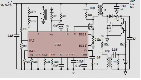
Instead of using a parts intensive secondary-side voltage reference and error amplifier to drive an opto-coupler, the primary bias winding on the flyback transformer [2] (T1) is used (Fig. 1). Proprietary feedback circuitry inside the LT3825 reads the reflected output voltage information on this winding during the flyback pulse. This voltage is then compared to a precision internal reference and an error signal is obtained. The error signal is used to modulate the on-time of Q1 [4] in such a way as to regulate the output voltage. An important benefit of this technique is that output voltage information arrives at the controller instantly after the
switching cycle is terminated. In a conventional optocoupler-based design, delays of tens to hundreds of microseconds occur in the opto-coupler alone, severely limiting the converter’s transient response. The synchronous rectifier output (SG pin) of the LT3825 makes driving the synchronous rectifier MOSFET (Q2) simple while maintaining a low parts count. Setting the dead-time of Q2 relative to Q1 only requires one resistor to program. Avoiding traditional, more complicated discrete timing circuits allows the designer to set optimum dead-times since this timing is well controlled within the LT3825. The LT3825 also precludes the need for a secondary-side synchronous controller IC and its associated circuitry. An optional, resistor programmable, input under voltage lockout is available. The slew rate of the output voltage during start-up can be controlled with an optional soft-start capacitor; this also limits the inrush current of the input power supply. Since the LT3825 incorporates current mode control, both short-circuit behaviour and ease of loop compensation are improved over voltage control schemes. Switching frequency is selectable from 50kHz to 250kHz optimizing the solution size vs efficiency. The switching frequency can be synchronized to an external system clock for further flexibility.
Figure 1. Circuit diagram
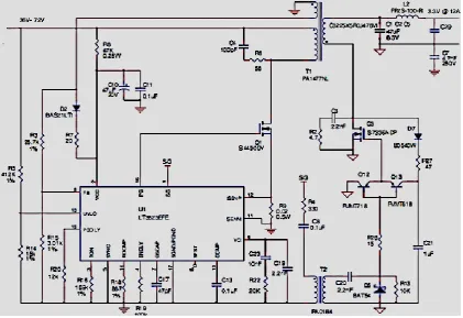
IV. SIMPLIFIED CIRCUIT DIAGRAM
Figure 2. Simplified diagram drawn using orcad capture
V. TEST RESULT
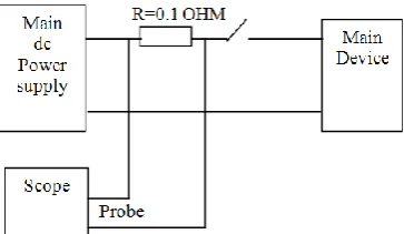
Fig. 3 shows the measurement equipment setup and when measuring the input or output voltage ripple, care must be taken to avoid a long ground lead on the oscilloscope probe. Fig. 4 shows the measurement set up for ripple voltage.
Figure 3. Measurement set up
Figure 4. Set up ripple voltage measurement
A. Load Regulation
To get maximum load, a rheostat was connected externally to the output of the controller (Table I). From
Fig. 5 and Fig. 6 the load variation matches the device behaviour. Input voltage is -48v.
TABLEI. LOAD VS OUTPUT VOLTAGE
Load (Amp) Input current (Amp)
Output voltage (V)
Efficiency (%)
0 0.024 3.369
2 0.168 3.366 83.48
4 0.318 3.364 88.15
6 0.473 3.362 88.84
8 0.629 3.360 88.03
10 0.790 3.359 88.58
12 0.955 3.356 87.85
Efficiency Vs Load current
83 84 85 86 87 88 89 90
0 2 4 6 8 10 12 14
load current(A)
E
ff
ic
ie
nc
y
(%
)
Figure 5. Graph for load current vs efficiency
Out put Voltage Vs Load current
3.355 3.36 3.365 3.37
0 2 4 6 8 10 12 14
Load current(A)
O
ut
put
V
ol
ta
ge
B. Line Regulation
Input voltage was varied from 36V to 72V at Maximum load=12.00A and corresponding output voltage was measured as shown in Table II.
TABLEII. VOLTAGES VS LOAD CURRENT
Input Voltage(V) Input Current(A) Output Voltage(V)
36.50 1.294 3.377
37.28 1.252 3.379
38 1.231 3.377
40 1.162 3.371
45 1.022 3.360
48 0.954 3.354
55 0.826 3.342
60 0.755 3.337
65 0.695 3.333
72 0.627 3.327
Fig. 7 represents the line regulation curve where the output voltage of the controller reaches its desired value 3.3V after 36V input voltage as expected from the device [1].
Out put Voltage Vs Input voltage
0 1 2 3 4
0 10 20 30 40 50 60
Input voltage
O
ut
put
V
ol
ta
ge
Series1
Figure 7. Variation input voltage vs output voltage
C. Ripple Voltage Measurement
Ripple voltage is 14.8mV at no load condition and 31.0 mV at full load condition i.e., at 12 Amp (as shown in Fig. 8 and Fig. 9). All voltages are within range.
D. Input Voltage vs Input Current
Fig. 10 shows the variation of input voltage and input current and nature of the curve as expected from the device. The corresponding input voltage and input current were measured as shown in Table III.
Figure 8. Ripple voltage at no load condition
Figure 9. Ripple voltage at full load condition (12A)
Input Voltage Vs input current
0 0.5 1 1.5
0 10 20 30 40 50 60 70
Input Voltage
inpu
t
c
ur
re
nt
Figure 10. Input voltages vs Input current
TABLEIII. INPUT VOLTAGES VS INPUT CURRENT
Input Voltage (V) Input Current (A)
36.50 1.294
37.28 1.252
38 1.231
40 1.162
45 1.022
48 0.954
55 0.826
60 0.755
65 0.695
72 0.627
E. Inrush current measurement
Experimental set up for measurement of inrush current is shown in the Fig. 11. Voltage across R=0.1 Ω is measured immediately during switch on condition and voltage is captured by scope (Fig. 12).
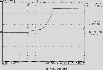
F. Output Voltage Tracking
From Fig. 13 the output tracking time is 3.48ms as expected from the device behaviour.
Figure 12. Inrush current measurement at full load
Figure 13. Rise time measurement
VI. CONCLUSION
The LT3825 allows a designer to improve the performance of isolated fly back circuits while lowering parts count, simplifying implementation and eliminating the need for an opto isolator. Special care was taken in PCB layout to keep the traces that conduct high switching currents short, wide and with minimal overall loop area.
Electric field radiation was lowered by minimizing the length and area of traces.
REFERENCES
[1] LT3825 Synchronous Flyback Controller with Wide Input Supply Range –data manual , Linear Technollogy, pp.1-5, 7, 25-29. [2] PA1477NL High Frequency Wire Wound Transformer data
manual, PULSE, pp.1-5.
[3] PA0184Pulse Transformer 1:1 1500Vrms 0.91Ohm Prim. DCR 0.91Ohm Sec.data manual, PULSE.
[4] Si4490DYN-CHANNELMOSFET data manual, VISHAY SILICONIX.
[5] FMMT718TA PNP Transistor-data manual, ZETEX. [6] FMMT618TA NPN Transistor-data manual, ZETEX
Chittajit Sarkar received B.Sc. (physics Hons.) degree from Ramakrishna Mission Residential College, Narendrapur, University of Calcutta in 1988, B.Tech and M.Tech degrees in Radio Physics and Electronics, University of Calcutta. He has served LOOP
TELECOM INC.TAIWAN;