Available Online at www.ijpret.com
238
INTERNATIONAL JOURNAL OF PURE AND
APPLIED RESEARCH IN ENGINEERING AND
TECHNOLOGY
A PATH FOR HORIZING YOUR INNOVATIVE WORK
EXPERIMENTAL REALIZATION OF MULTIPLE ALL OPTICAL UNIVERSAL
LOGIC GATES USING ARRAY ILLUMINATOR
PRAFULL P PADGHAN, KAMLESH ALTI*
Department of Physics, Sant Gadge Baba Amravati University, Amravati – 444602, Maharashtra, India.
Accepted Date: 27/02/2014 ; Published Date: 01/05/2014
\
Abstract: This paper describe the experimental realization of multiple all optical NOR and NAND logic gates using array illuminator. Two Michelson interferometers in tandem were used to produce four nearly collinear beams. Interference of these four beams yield square arrays of equal illuminating light spots. Detectors placed at strategic locations in the interference pattern for sensing light have truth table matching with NOR and NAND logic gates when the beams from the interferometers were blocked and unblocked sequentially. Previous reports of the fabrication of optical logic gates utilize various nonlinear optical
phenomena whereas in this work only linear optics was used.
Keywords: Array Illuminator, multiple beam interference, optical logic gates.
Corresponding Author: MR. PRAFULL P PADGHAN
Access Online On:
www.ijpret.com
How to Cite This Article:
Available Online at www.ijpret.com
239
produce the nano-deposition [6], online optical testing, etc. Different applications require different types of array illuminator. Various methods have been proposed to produce AIL using diffraction techniques [7, 8] and interference technique [9]. In all, these diffraction based techniques the geometry and size of the arrays are dependent on the diffracting element, without having much scope of online control. To realize the arrays of different configuration, different diffractive elements have to be designed and used accordingly. An array illuminator can be achieved via interference of multiple nearly collinear beams. In this technique the spot size, the array size and the compression ratio of the array pattern can be varied in real time. By the relative orientations of the appropriate mirror, the geometry of arrays can be easily controlled. Recently there has been a proposal to use interferometer array illuminator for the realization of all optical logic gates [10]. An optical logic gate is a switch that controls one light beam with another. It is "on" when the device transmits light, and "off" when it blocks the light. All optical transistors and logic gates similar to electronic transistors and logic gates respectively are the basic building blocks of a photonic chip. Generally optical logic gate can be realized via two methods; one is using semiconductor optical amplifier (SOA) with Mach-Zender interferometer (MZI) [11] and other is using the nonlinearity of optical fibre [12]. Other variants utilize various kinds of nonlinearity to realize the optical logic gates. Processing, storage, transport and visualisation of huge amounts of data at ultra high speed have been possible using photonics technology.
This paper discusses an experimental realization of all optical multiple universal logic gates using array illuminator obtained via four beam interference method.
Experiment Set up:-
Available Online at www.ijpret.com
240
Fig.1: Schematic of experimental set up
Beam splitters BS1, and mirrors M1 and M2 form the Michelson interferometer giving the two
interfering beams. These two beams can be launched into the second stage, a second Michelson interferometer, comprising of beam-splitter BS2 and mirrors M3 and M4. Thus the
output of BS2 consists of four nearly collinear interfering beams. The mirror tilts can be adjusted
in such a way that the interference patterns of individual stages were oriented perpendicular to each other. Interference pattern can be recorded using CCD camera. Characterization of interference pattern such as number of spots, periodicity and their contrast can be measured using the image captured in CCD camera. Four beams interferometer can be easily brought down to a two beam interferometer by blocking the beam at appropriate locations using electronically controlled two mechanical choppers C1 and C2. The resultant intensity distribution
of four beam interference pattern generated by using such a set up is given by [4-5]
) 1 ( )] cos( 2 ) cos( 2 ) cos( 4 ) cos( 4 4 [
0
I kx ky kx ky kx ky
I
Where k=2πµ spatial frequency θ is angular separation between the two interfering
beam and it is of the order of 1 mrad. λ is the wavelength of laser light used. Fig. 2 shows the
computed plot of intensity distribution of Eq.1. Beam profiler (BC 106-VIS, Thorlabs Beam 4.0)
was used to record the interference pattern/output of the BS2. Imagine there are four zones in
the pattern of Fig.2 and detectors are placed at these locations namely D1, D2 D3 and D4. The
Available Online at www.ijpret.com
241
Fig. 2: Simulated Four beam interference pattern.
Results and Discussions:-
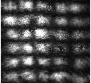
Fig. 3 shows the resultant pattern of four beam interference. Arrays of equal illuminating light spots in the square geometry are seen in Fig. 3.
Fig. 3: Four beam interference pattern.
Now if chopper kept in the front of M2 is blocked then, we will get interference of only two
Available Online at www.ijpret.com
242
Fig.4: Interference pattern obtained when the beam going to M2 is blocked.
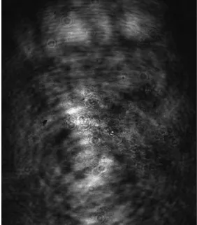
Similarly when the beam going towards M3 was blocked we obtained again two beam interference pattern as shown in Fig. 5.
Fig.5: Interference pattern obtained when the beam going to M3 is blocked.
If both the beam going towards M2 and M3 were blocked no interference pattern was obtained
Available Online at www.ijpret.com
243
Fig.6: CCD output obtained when both choppers were blocking the beam.
Now we will probe the intensity of light at the zones marked by D1, D2, D3 and D4 in Fig.2.
Imagine there four tiny photo detector kept in these places. Now let us see the intensity variation at these four points.
Starting with imaginary detectors kept at D1. Now let us consider the output of the detector
placed at maxima (bright spots, D1 as shown in Fig. 3). When C1 and C2 both are at OFF position
i.e. they allow laser beam to pass through them (1, 1), this will yield four beam interference
pattern as shown in Fig. 3. Light will get detected at D1 and hence it implies to ‘ON’ state (1).
Suppose one of choppers is blocking the beam (1, 0) or (0, 1), then it will yield two beam interference which again corresponds to light at D1 and hence a ‘ON’ state (1). Even if both
choppers C1 and C2 are blocking the beams still D1 will get illuminated with laser beam reflected
from M2 and M4. Hence (0, 0) will yield ‘ON’ state (1). This discussion is tabulated in Table 1.
Hence outputs of D1 do not correspond to any logic gate.
Table No. 1: Output of the imaginary detector placed at D1
Input Output
1 1 1
1 0 1
0 1 1
0 0 1
Consider the output of the detector D2 placed at the horizontal minima as shown in Fig.2. For all
Available Online at www.ijpret.com
244
state (0). When both the choppers are blocking the beam, laser beam will get reflected from mirrors M2 and M4 and D2 will get illuminated. This discussion is tabulated in Table 2.
Table 2: Output of the imaginary detector placed at D2
Input Output
1 1 0
1 0 0
0 1 0
0 0 1
Hence output of D2 corresponds to NOR logic gates. Now let us consider the output of the
detectors D3 and D4 combined together. When both choppers are not blocking the beams
coming towards mirrors M2 and M3, light will not get detected at D3 and D4. Hence output for
will be (0, 0) and combined output will be zero. At (1, 0) detector D3 will get illuminated with
light since two beam interference pattern will be vertical as seen in Fig. 5 and hence output at D3 will be 1. Whereas output of D4 will be 0 for (1, 0) output and combined output of D3 and D4
will be 1. At (0, 1) detector D4 will get illuminated with light since two beam interference
pattern will be horizontal as seen in Fig. 4 and hence output at D4 will be 1. Whereas output of
D3 will be 0 for (1, 0) output and combined output of D3 and D4 will be 1 again. For (0, 0), output
of combined D3 and D4 will be again 1 as both the detectors will receive light.
Table No. 3: Output of the imaginary detectors placed at D3 and D4 combined together.
Input Output
1 1 0
1 0 1
0 1 1
0 0 1
CONCLUSION:-
Utilization of such interference pattern to realize optical logic gate has some advantages. First of all several optical logic gates can be realized simultaneously in a single interferometer beam without using any nonlinearity. It is reported [9] that one can generate the matrix of around 20×20 tiny spots with very good contrast. The highest recorded spot density in the patterns was
around 900 mm2. So an interference pattern is equivalent to an optical chip having many logic
Available Online at www.ijpret.com
245
3. Liren Liu, Xiaoben Liu, Bo Cui. Optical programmable cellular logic array for image processing.
Appl Opt 1991;30(8):943–9.
4. Morrison RL, Walker SL, Cloonan TJ. Beamarray generation and holographic interconnections
in a free-space optical switching network. Appl Opt 1991;32(14):2512–8.
5. Liao TD, Stephen Sheard. Integrated-optic array illuminator: a new design for guided-wave optical interconnections. Appl Opt 1998;37(13):2729–34.
6. Sandoghdar V, Drodofsky U, Schulze Th, Brezger B, Drewsen M, Pfau T, Mlynek J. Lithography
using nano-lens arrays made of light. J Mod Opt 1997;44:1883–98.
7. Hamam H. Talbot array illuminator: general approach. Appl Opt 1997;36(11):2319–27.
8. Lohmann AW, Thomas JA. Making an array illuminator based on Talbot effect. Appl Opt
1990;29(29):4337–40.
9. A S Patra and Alika Khare, Optics & Laser Technology, 38, (2006) 37.
10. K Alti, P Chapate, K Singh, Simultaneous Realization of Multiple NAND Optical Logic
Gates using four Beam Interferometer, International Journal of Basic and Applied Research, 103-105 (2012).
11. Joo-Youp Kim, Jeung-Mo Kang, Tae-Young Kim, and Sang-Kook Han, "All-Optical Multiple
Logic Gates With XOR, NOR, OR, and NAND Functions Using Parallel SOA-MZI Structures: Theory and Experiment," J. Lightwave Technol. 24, 3392 (2006).
12. J.-M. Jeong, M.E. Marhic, "All-optical logic gates based on cross-phase modulation in a