Copyright © 2013 IJECCE, All right reserved
Optimization of Real Time Application on Mixed
Architecture Using AAA Methodology Extension
O. Feki, T. Grandpierre, N. Masmoudi, M. Akil and Y. Sorel
Abstract – Mixed Architectures contain programmable devices and reconfigurable devices. They provide a powerfull answer to meet the computational requirement of latest digital signal processing applications. But the complexity of the corresponding algorithms and the multiplicity and diversity of computing components usually lead to a huge number of possible implementations. Architecture Algorithm Adequation (AAA) is one of the rapid prototyping methodologies which allow to explore the solution set to build an optimized application. However, it requires improvement in order to support mixed architectures containing both programmable and configurable components. This paper suggests an extension of the AAA methodology to support mixed architectures. The AAA architecture model is first extended to mixed architecture. Then, we present the coupling of existing tools (SynDEx and SynDEx-IC) in order to support mixed architectures. Finally a communication IP is proposed to manage FPGA communication and its synchronization with other components of the mixed architecture.
Keywords – Rapid Prototyping, AAA, Co-Design, Real-Time, H264.
I. I
NTRODUCTIONDigital signal processing uses more and more complex algorithms to perform better and innovative functionalities. This complexity growth goes hand in hand with the increasing computing demand. Unfortunately, single-processor systems cannot meet this demand. Therefore system designers use multi-component heterogeneous systems containing different types of computation components interconnected by different types of communication media. These computation components can be programmable circuits (DSP, RISC, CISC ...) or reconfigurable circuits (FPGAs …). In the following, we refer to architectures which contain programmable devices and reconfigurable devices as mixed architectures. Optimizing algorithm implementation on these mixed architectures means finding a compromise between temporal performances and used logic blocks number. Indeed, increasing parallel computation leads to latency decrease in return of used ressources increase.
Using Mixed Architectures for complex algorithms leads to a huge number of possible implementations which requires long time to be explored. Consequently, rapid prototyping methodologies and their associated tools must be used to obtain an efficient implementation in the least possible time. Among these tools, CoFluent [1] and PtolemyII [2] allow complex architecture modeling and functional simulation, ASTEX [3] permits repetitive extraction of codelets whose execution on coprocessors can accelerate application execution time. Diamond 3L [4] permits code generation for applications on mixed
architectures based on TI DSPs and Xilinx FPGAs. It also generate necessary communications. Bourgos et al. [5] propose a method to model algorithms and multiprocessor architectures for the sake of simulation only. Finally, none of mentioned tools perform automatic partitioning or optimizations on the target architecture. On the contrary, Gedae [6] and DOL [7] perform automatic scheduling but only on multiprocessor architectures. ECOS [8] allows scheduling minor complexity algorithms on mixed architectures, but it cannot deal with real life algorithms. CODEF [9] is a tool which permits scheduling algorithms on mixed architectures, but the description that it uses is fine-grained, which requires much time to perform specifications and scheduling. The Algorithm Architecture Adequation (AAA) [10] methodology targets multiprocessor architectures. It was previously extended to target reconfigurable architecture but it does not yet cover the mixed architectures.
This paper presents our AAA methodology extension and is organized as follows: section II presents the AAA methodology foundation. It presents the models used to specify the application algorithm, programmable architectures and reconfigurable architectures. It also exposes optimization heuristics and software tools supporting AAA methodology (SynDEx and SynDEx-IC). Section III, is dedicated to our AAA methodology extension. It presents the AAA models extension and our new software tool based on the coupling of SynDEx and SynDEx-IC. It finally details the automatic synthesis of communication between programmable and reconfigurable parts of the architecture. Section IV describes an actual concretization of the obtained result and in section V a conclusion is provided and perspectives are drawn.
II. AAA M
ETHODOLOGYF
OUNDATIONAAA [11] is a rapid prototyping methodology that has been developed to help real-time system designers to implement and optimize their algorithms on multicomponent architectures. AAA is a formal methodology based on graphs transformations in order to build an executable implementation. AAA is devised for programmable and ASIC components. It is implemented in the SynDEx software tool [10].
Copyright © 2013 IJECCE, All right reserved Further investigation allowed a specific extension to the
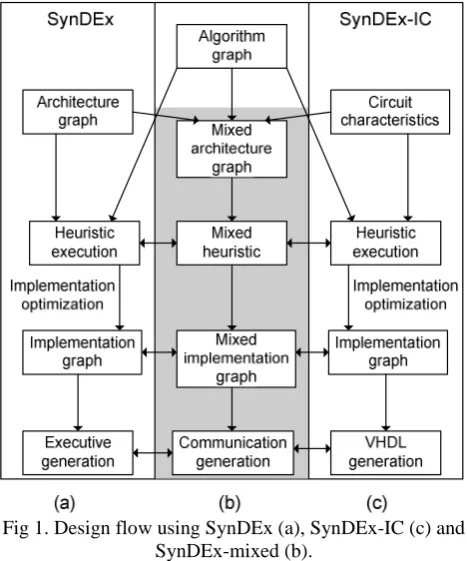
deployed methodology that supports reconfigurable circuits. This extension has led to SynDEx-IC that target mono FPGA archictecture[12]. SynDEx-IC optimizes the algorithm graph implementation on reconfigurable components (FPGA) by using a dedicated heuristic in order to reduce both the execution time and the number of logical blocks of the FPGA. Finally, it generates the corresponding VHDL code (figure 1-c) that feeds the usual synthesis tools.
In this paper we target mixed architecture made of programmable and reconfigurable components. The grayed part in figure 1-b exposes the proposed design flow extension of AAA presented in this paper.
Fig 1. Design flow using SynDEx (a), SynDEx-IC (c) and SynDEx-mixed (b).
Both AAA for programmable circuits and AAA extension for reconfigurable ones are based on the same algorithm model. Algorithm is modeled by a graph (O, D) where O is the set of vertices and D is the set of edges connecting them [12]. Each vertex of O is an operation of the algorithm and each edge of D represents data dependency between a producer operation and one or more consuming operations. Operations correspond either to a subset of instructions or to a circuit (an ASIC or a VHDL component).Vertices can be of five types: constant, sensor, actuator, delay or function.
Figure 2-a shows the algorithm graph computing the average value of two input sensors (a and b) using two operations (addition and division) and one constant (2). Vertex C is the output actuator (a display for example) Most of signal processing algorithms are based on repetitive operations. We introduce the finite factorization feature of AAA which allows the simplification of their presentation. Factorization is the representation of a set of repetitive computing operations by a single pattern and marking each edge crossing the pattern frontier with a
special factorization vertex. Depending on the way the data are managed when crossing the factorization frontier, factorization vertices can be: a fork node, a diffuse node, a join node or an iterate node [10]. Figure 2-b is a non factorized graph for matrix (3x3) vector (of size 3) product. Figure 2-c is the corresponding factorized graph. The node V represents the scalar product of two vectors.
Fig.2. Algorithm graph example
Factorization does not only reduce the specification size, but it also allows distinguishing specification and implementation. From such factorized specification, it is possible to realize a fully parallel, fully sequential or any intermediate implementation.
AAA addresses reactive real-time systems that react with their environment in a discrete form of an infinite repetition of a sequence acquisition-computation-action. By analogy with the finite factorization, we introduce the infinite factorization frontier which is a border that includes the entire algorithm (the sequence acquisition-computation-action). It models the system’s interaction with its environment
In this section, we have presented the algorithm model common to SynDEx and SynDEx-IC. In the following, we present SynDEx and SynDEx-IC specificities in detail.
A.
AAA methodology
for
programmable
component: SynDEx
AAA methodology helps distributing and scheduling real time application on heterogeneous multi processor systems using the presented algorithm model and the architecture model indicated below.
1)
AAA Architecture model
Copyright © 2013 IJECCE, All right reserved This model is based on a graph (S, A) where S is the set
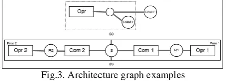
of vertices and A the set of edges connecting them. Each element of S is a finite state machine that can belong to one of four groups: operators (executing computing operations), communicators (executing data transfer operations), bus/mux/demux and memories (used for storing data). The operator models arithmetic and logical units and the communicator models a DMA channel. Then a processor is modeled by one or more operators connected to one or more memories. It can optionally contain communicators.
Fig.3. Architecture graph examples
As an example, figure 3-a depict a mono-processor architecture connected to two RAM memories. The empty circle between the operator and the memories represents the Bus/mux/demux used to switch access to memories. Figure 3-b presents a message passing architecture made of two processors. This example exhibits communicators nodes (Com1 & Com2) which are used to execute data transfers between the local memories R1 and R2. Communications are realized through a FIFO modeled by the Sequential Access Memory node ‘S’. More examples of architectures are given in [10].
2)
AAA-Implementation graph
Exactly one operator is required to execute one operation; and for every operation of the algorithm graph there must be at least one operator of the architecture graph able to perform it. If several operators are able to perform an operation, one of them must be chosen to execute it (as explained in the following subsection). When two operations are in data dependence, the producer operation must be executed before the data consumer operation. When two data dependent operations are not executed by the same operator, the data must be transferred from the operator that executes the producer operation to the operator that will execute the consuming one. To accomplish this data transfer, a path connecting these two operators must be chosen in the architecture graph. Once one is selected, on each node of the path (memory, bus/ mux/demux, communicator), a corresponding allocation node (memory allocation, transfer) is added to the algorithm graph. This transformed algorithm graph is called an implementation graph.
For a pair of graphs (algorithm and architecture) there are a large but finite number of possible implementations graph. The top, center and bottom of figure 4 depicts respectively an algorithm graph, an architecture graph, and a possible implementation graph. This latest graph highlights the distribution and scheduling of algorithm’s operations on each operator of the architecture. “Alloc”, “R” and “S” nodes are added during the distribution and scheduling process in order to exhibit the allocation of memories and the execution of data transfert (send and receive operations).
Fig.4. algorithm graph and correspondent implementention graph on dual processor architecture communicating
through a FIFO (SAM node)
3)
AAA Optimization heuristic
For embedded applications, designers are asked to make time efficient systems using the least possible resources. The set of possible implementations is huge and this optimization problem is known to be NP-complete. To avoid exploring the whole solution set, we use heuristics. AAA heuristic is based on a greedy list scheduling algorithm with a cost function considering the execution of operation and communication durations. To estimate the execution duration of the algorithm, every operation of algorithm graph must be characterized by its execution duration on each operator able to perform it. The execution duration of an operation “o” on the operator “opr” is noted δ (o,opr).
At each heuristic iteration, a list of schedulable operations is built: a schedulable operation is an unscheduled operation of algorithm graph which has no predecessors or whose all predecessors are scheduled. For each operation on the heuristic list, we associate the best operator which minimizes the operation end date. This operator is designated as the best operator of the operation. Among this list, we choose to schedule the operation Oi which maximizes the cost function σ(Oi)=P(Oi)-F(Oi) on
its best operator. P(Oi) is the scheduling penalty; it
corresponds to the critical path length increase due to the operation Oischeduling. F(Oi) is the scheduling flexibility
of the operation Oi. It is the difference between the
smallest possible starting date of the operation Oiand its
Copyright © 2013 IJECCE, All right reserved 4) AAA Code generation
Once the optimized implementation is obtained, we can move to executive generation. Several source files are generated [10]: one for each operator and one for automating the compilation chain. Each operator executive contains a list of calls to be translated by macro-processor into source code in the compliable language of the targeted operator.
5) AAA Supporting tool: SynDEx
The AAA methodology is implemented in the CAD software SynDEx [13]. The user specifies the algorithm (fig 5-b) and architecture graphs (fig 5-a) thanks to SynDEx graphical interface. Then the user runs the optimization heuristic and get a temporal diagram (figure 5-c) of the distribution and scheduling. If the obtained implementation meets the system designer constraints, SynDEx can generate the corresponding executives. If not, the user the graphical interface allows the user to add some heuristics constraints or to modify the graphs.
Fig.5. Architecture graph, algorithm graph and temporal graph from SynDEx
B. AAA methodology extension to reconfigurable
circuits: SynDEx-IC
More and more circuit designers choose hardware implementation to fill high performance demand. But, initially AAA methodology was created to deal with the algorithm scheduling problem for multiprocessor architectures. Therefore, it was extended in order to solve the hardware implementation optimization problem in the case of a unique FPGA target architecture [12]. This extension aims at building an implementation which meets the time constraint (or approaches it if not possible) using the least possible resources. In the following paragraph, we expose the optimization heuristic and code generation method used in this AAA extension to reconfigurable circuits and its supporting tool SynDEx-IC.
1) AAA circuit : Optimization heuristic
AAA methodology extension to reconfigurable architectures exploits FPGA parallelism by unrolling loops which have not inter iteration dependencies. So, algorithm latency is reduced in exchange of increasing hardware resources. Given an algorithm graph, the characteristics of a targeted FPGA and a temporal constraint, a dedicated optimization heuristic is deployed to choose the factorization frontiers to unroll. This heuristic use a list of candidate frontiers which are the ones on the critical path. Then for each frontier of this list, the heuristic compute the “greatest factorization degree” : it is the value implying the minimum critical path length or one lower than the time constraint. Finally a cost function is calculated for each couple (factorization frontier, optimal factorization degree). The couple that most minimizes this cost function
is selected, the frontier deleted from the list and a next iteration can start until the critical path become less or equal to the specified temporal constraint.
2) AAA circuit : Code generation
The final circuit is made of two parts that are automatically generated: data path and control path.
The data path synthesis is built by replacing each vertex of the algorithm graph by an operator and each data dependency by an operator connection. This asserts that there is an operator type for each algorithm graph vertex type. These operators can be either a hardware component of a VHDL library for an arithmetic operation node, a multiplexer for the “fork” factorization node, a demultiplexer for the factorization ”join” node or a register for the “Iterate” vertex.
Copyright © 2013 IJECCE, All right reserved
3) AAA circuit supporting tool: SynDEx-IC
The extension of AAA methodology for reconfigurable circuits is implemented in the CAD software tool SynDEx-IC [14]. Its graphical interface allows the user to specify the algorithm graph, the target FPGA proprieties and the time constraint. Then it allows to run the defactorization heuristic and to generate synthesizable VHDL. Finally, the user uses the classical synthesis tools (ISE, Quartus …) to generate theFPGA configuration.
III. AAA M
ETHODOLOGYE
XTENSION TOM
IXEDA
RCHITECTURESThe previous sections were devoted to the two existing software tools based on the AAA methodology: SynDEx for programmable circuits and SynDEx -IC for reconfigurable circuits. This section presents our AAA extension and the associate tool that allows to target mixed architectures made of both programmable and reconfigurable components.
On the one hand, SynDEx is used to distribute and schedule algorithm operations on each operators. On the other hand, SynDEx-IC is able to optimize the implementation of operations scheduled on reconfigurable components thanks to loop unrolling. There is no need to modify the algorithm model since it is the same on both side. On the contrary, it is necessary to make an extension of the AAA architecture model in order to exhibit the parallelism offered by the FPGA so that it could be used by SynDEx.
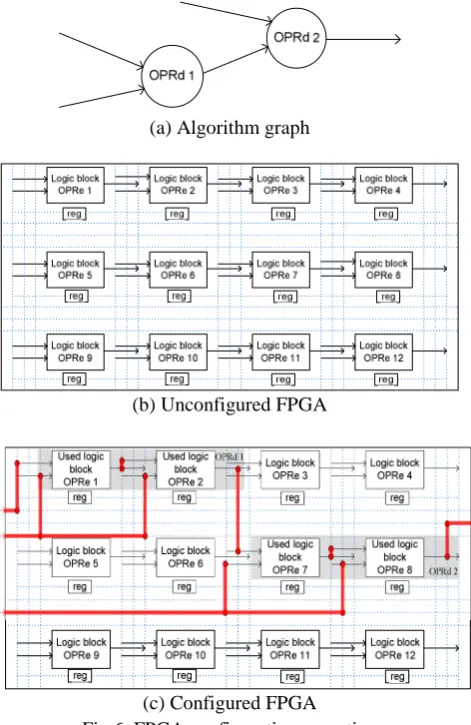
A. Model extension: FPGA model
FPGAs are made of a matrix of configurable logic blocks (to perform combinatorial and sequential functions) and RAM blocks surrounded by input and output blocks. They are all connected by a programmable interconnection network made of electric lines and fuses that can be connected or disconnected during the configuration phase. The configurable logic blocks are modeled by a set “SOPRe” of vertexes named elementary operators“OPRe”. RAM blocks are modeled by a set of vertex “Sreg” of
registers. The programmable network is modeled by a network “R” of edges. Therefore, an unconfigured FPGA is modeled by a graph GFPGA= (SOPReSreg, R).
FPGA configuration is performed in two steps by synthesis tools: configuration of the logic blocks, and configuration of the connection network.
Starting with an unconfigured FPGA, the configuration process transform elementary operators and registers into a set “SOPRd” of degenerate operators (OPRd): a degenerate
operator is an operator able to perform only one operation of the algorithm graph. It is made of a set of configured elementary operators and RAM memories connect by a configured connection network. In the following, the function ρ models the configuration applied to an unconfigured FPGA.
where S’OPRe, S’regand R’ correspond to respectively the
set of elementary operators, the registers and the part of the interconnection network used to obtain the set of degenerate SOPRd.S’’OPRe, S’’regand R’’ correspond to the
set of elementary operators, registers and the part of the interconnection network which are still not configured. Figure 6-a presents a basic example of algorithm graph made of two operations A and B which have to be implemented on the unconfigured FPGA of figure 6-b. Finally the figure 6-c presents the configured FPGA. In this last figure the configuration process build two degenerated operators “OPRd1” and “OPRd2” that will respectively able to execute operations A and B. We can observe that “OPRd1” rely on the elementary operator OPRe1 and OPRe2, while OPRd2 rely on OPRe7 and OPRe8. Finally the interconnection network configuration (bold red edges of figure 6-c) connect the degenerated operators.
(a) Algorithm graph
(b) Unconfigured FPGA
(c) Configured FPGA Fig 6. FPGA configuration operation
Copyright © 2013 IJECCE, All right reserved
B. SynDEx/SynDEx-IC heuristics coupling
The previous models are used internally by SynDEx. From the user side, the graphical insterface allows the user to specifies algorithm graph GAL and architecture graph
GAR. GALis the set of the operations (O1, O2,…,Oq) and
data dependences of the application algorithm. GARis the
set of programmable operators (opr1…oprn), FPGAs
(FPGA1…FPGAm) of the target architecture, including the
communication mediums connecting them (com1…comp).
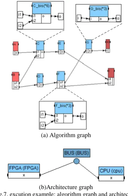
At this point it is important to notice that each FPGA is simply specified using a single node. For example, figure 7-a shows an algorithm graph example. This graph is made of 9 operations among which operations C, F and G encapsulate repetitions.
(a) Algorithm graph
(b)Architecture graph
Fig.7. excution example: algorithm graph and architecture graph specified by user
Figure 7-b shows the initially specified architecture graph. This architecture graph is made of 2 operators: one programmable (processor) and one reconfigurable (FPGA). The user has also to fill a table (table 1) that specify the worst case execution duration of each operation on each operator able to execute it. One can see that for this simple example, the processor is able to perform all operations of the algorithm graph while the FPGA is able to perform only the operations C, F and G. For the FPGA theses duration correspond to a fully sequential execution (factorized graph).
Table 1. initial operation duration on each operator
Processor FPGA
A 1
B 1
C 9 7
D 2
E 1
F 6 4
G 8 5
H 1
I 1
Since SynDEx does not consider FPGA potential parallelism we need to expose this parallelism in SynDEx before we can couple heuristics. For this purpose we apply the algorithm 1 to the couple of input graph (algorithm and architecture). It transforms the architecture graph by replacing each FPGA of the initial architecture graph by the set of degenerate operators it may contain: the FPGA node is deleted from Gal, and for each operation schedulable on the FPGA, a degenerate operator is added. This exhibits explicitly the internal FPGA parallelism. Inputs: GARand GAL
Outputs: transformed GAR
1: for each FPGAi∈GAR
2: FPGAi’={}
3: for each FPGA connection with other components 4: FPGAi’= FPGAi’ + {com-IP}
5: end for each
6: for each operation O∈П’-1(FPGAi)∩ GAL
7: FPGAi’= FPGAi’ + OPRd(O)
8: end for each
9: FPGAi’= FPGAi’ + cominternal
10: FPGAi= FPGAi’
11: end for each
Algorithm 1: heuristic for mixed circuit
This transformation applied to the architecture graph given figure 7-b would produce the architecture graph given figure 8 with the 3 degenerative operator nodes “OPRd_C”, “OPRD_F” and “OPRd_G”. It is also important to notice that a communication node “COM_IP” is inserted between the FPGA and theses new degenerative operator nodes. This communication node models the serialization of the FPGA communication with the other components of the architecture graph (inter-FPGA communications). Finally, we model the configurable connection network of the FPGA (intra-FPGA communications) by a multi point SAM with no cross time for all data types: setting a cross time to zero is effectively equivalent to a completely connected network.
Copyright © 2013 IJECCE, All right reserved Step 1: SynDEx its optimization heuristics to distribute
and schedule the algorithm graph operations on the operators of the transformed architecture. At this level, factorization frontiers are scheduled sequentially even on FPGA. Applied to figure 7-a algorithm and figure 8 architecture graphs, SynDEx build the implementation graph of figure 9 (operators and communication are displayed horizontally on the top, while operations scheduled on each operators and media are displayed vertically).
Fig.9. implementation graph after GARtransformation
Step 2: SynDEx-IC heuristic is use to optimize the implementation of sub graphs distributed on each FPGA operator, but it only deal with operations that belong to the critical path of the implementation graph. As previously explained, SynDEx-IC will search for the optimized defactorization degree for each of these operations. This optimization is done in two steps:
a)
Execution time minimization: SynDEx-IC will unroll all factorization frontiers. To do so, for each sub graph we take the proprieties of the FPGA on which it is distributed. Those FPGA proprieties are the execution time and the used surface for each operation it can perform. They are specified by the user when defining the architecture graph. Given FPGA proprieties, the sub graph and the time constraint (C=1), SynDEx-IC calculates the smallest execution time of the sub graph. Figure 10 presents the resulting implementation graph of the figure 7 example.Fig.10. Implementation graph after execution time optimization
b)
Space minimization: this step focus on CLB reduction without increasing the critical path (CP) length. So doesn’t optimize space for sub graphs containing operations on the CP. So each sub graph previously optimized is considered as a single operation “OP” if it does not containoperations on the critical path. Duration of this operation is denoted “dOP”. Then SynDEx is used to compute calculate cost function named “schedule flexibility” [15]: SFOP it is thedifference between its latest start date which does not extend critical path and its earliest start date. This value is send back to SynDEx-IC which compute a new temporal constraint TCOP=dOP+SFOP and search for the optimize
defactorization degree. This temporal constraint guarantees that the critical path length does not increase. The final implementation graph corresponding to the example is shown on figure 11. We notice that C execution duration was increased due to space optimization without affecting the total execution duration.
Fig.11. Final implementation time
At this level, the optimization process is done and the final implementation graph can be used by SynDEx to generate the executives while each sub graphs are transformed into VHDL codes by SynDEx-IC. However, SynDEx-IC does not still generate components to manage communication and synchronization with programmable parts. This is the objective of the next section.
C. Communication IP generation
Copyright © 2013 IJECCE, All right reserved transformed to a sequence of data transfer functions call.
On FPGA side, the same sequence is used to configure a generic circuit that we present now.
The communication IP, presented in figure 12, is used for every connection between an FPGA and any other component. It is a degenerative operation able to send or receive data to or from other components in synchronization with operations executed on the FPGA side. This operation IP is composed of two parts: a data path and a control unit.
The data path consists of a multiplexer to specify the transfer orientation and registers. Unlike sent data, the registration of received data is needed to maintain a steady signal at the operator’s inputs. Then a multiplexer is necessary to switch data to be sent. Command signals for the multiplexer and the registers are generated by the control unit.
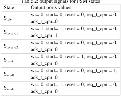
The control unit is made up of a finite state machine, package and data counters, a comparator, sent and received package counters, a multiplexer for received data register commands, a ROM memory (see hereunder) and synchronization unit “oprd_synch” with OPRd blocks.The FSM synchronizes the CPU communicator with the FPGA communicator. It has seven input ports: the clock (Clk) and initialization (init) ports, three ports for synchronization with OPRds and the CPU: req_f_oprd, req_f_cpu, ack_f_cpu, the port in_out which indicates the transfer direction and the end port which indicate the end of current data reception or sending. There are five output ports: ack_t_cpu and req_t_cpu for synchronization with CPU, wr for data writing enabling and two output ports to command the package counter (start to increase the value and reset to reset it). FSM operates as shown in figure 13 and output signals for each state are regrouped in table 2.
Copyright © 2013 IJECCE, All right reserved Fig.13. FSM functioning
Table 2: output signals for FSM states State Output ports values
Sidle
wr= 0, start= 0, reset = 0, req_t_cpu = 0, ack_t_cpu=0
Srecieve1
wr= 1, start= 1, reset = 0, req_t_cpu = 0, ack_t_cpu=1
Sreceive2
wr= 0, start= 0, reset = 0, req_t_cpu = 0, ack_t_cpu=0
Sreset
wr= 0, start= 0, reset = 1, req_t_cpu = 0, ack_t_cpu=0
Ssend1
wr= 0, start= 0, reset = 0, req_t_cpu = 1, ack_t_cpu=0
Ssend2
wr= 0, start= 1, reset = 0, req_t_cpu = 0, ack_t_cpu=0
The ROM is built from the scheduled sequence of communications performed by SynDEx during the distribution process. It contains at the ithaddress the packet number in the ithdata coded on n bits. The (n+1)thbit is used to indicate a send or a receive operation. And the (n+2)th bit is used to store acknowledgement or request sent to the OPRd. The synchronization with OPRd bloc has five input ports: synchro and in_out connected respectively to the (n+2)th and the (n+1)th bit of the ROM, en indicating the end of current data transfer and the req_f_oprd and ack_f_oprd. It has two output ports which are req_t_oprd and ack_t_oprd. If synchro=1 and in_out=0 then in rising edge of en, req_t_oprd=1, this value is maintained until the acknowledgment from OPRd (req_f_oprd ) is received. If synchro and in_out are equal to 1, then on en rising edge, the ack_t_oprd=1 and this value is maintained until req_f_oprd=0. To allow data transfer by packets, each packet is registered separately. Then we use the demultiplexer to switch the write (wr) signal to the appropriate register. The control signals for this demultiplexer and the send_pck_mux are the outputs of two counters which count respectively received and sent packages.
IV. V
ALIDATIONA. Description
In order to validate our optimization heuristic on a mixed architecture, we present the implementation of intra 16x16 prediction decision of H.264 video encoding algorithm [16]. This decision is made by comparing different predicted blocks using different prediction modes and the original frame block. The closest resembling predicted block is chosen. The most used graphic comparison criterion is the SAD (Sum of Absolute Difference); its equation (3) shows that it consists on a repetition of subtractions, absolute value and accumulation. Since all the iterations of the SAD operation are independent, they can be executed in parallel on a FPGA.
Nj N
i
SAD
1 1
j)
MBref(i,
-j)
MBcur(i,
(3)To simplify the algorithm, we consider three prediction modes [17]: DC mode, Horizontal mode and Vertical mode. The algorithm graph is shown on the figure 14.
Fig.14. intra 16x16 decision algorithm graph This algorithm has three inputs:
• SRC (256 uchar): the current macro bloc (16 rows of 16 pixels each).
• TOP (16 uchar): top neighborhood (1 row of 16 pixels).
• LEFT (16 uchar): the left neighborhood (1 column of 16 pixels).
The three outputs of this algorithm are the DC value (DC_val), the value of the minimum SAD found (min_SAD) and its correspondent mode (best_mode). This algorithm is based on five operations:
• Calc_dc_val: calculates the mean of the 32 neighbor values.
• SAD_dc: calculates the SAD of the DC mode prediction.
• SAD_v: calculates the SAD of the vertical mode prediction.
• SAD_h: calculates the SAD of the horizontal mode prediction.
SAD_comparator: compares the three calculated SADs and gives the smallest value and its correspondent mode (0 if vertical mode, 1 if horizontal mode and 2 if DC mode).
Copyright © 2013 IJECCE, All right reserved Fig.15. target architecture graph
The execution duration of each operation of the algorithm graph on architecture graph operators is shown on table 3 . Each operator can only execute operations for which the duration of execution is given.
Table 3: Operation duration on each operator
CPU FPGA
SRC 256
TOP 16
LEFT 16
Calc_DC_val 33 18
SAD_V 768 296
SAD_H 768 296
SAD_DC 768 296
SAD_comparator 38
DC_val 1
Min_SAD 1
Best_mode 1
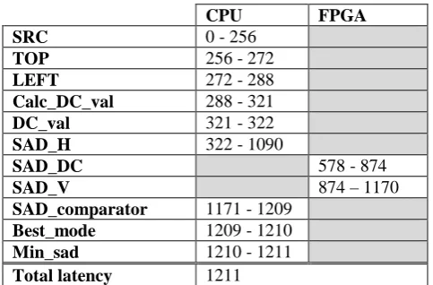
B. Schedulig using current SynDEx version
When we execute the initial (not modified) optimization heuristic of SynDEx on these graphs, we get the following results (table 4).
Table 4: sheduling result without architecture graph transformation
CPU FPGA
SRC 0 - 256
TOP 256 - 272
LEFT 272 - 288
Calc_DC_val 288 - 321
DC_val 321 - 322
SAD_H 322 - 1090
SAD_DC 578 - 874
SAD_V 874–1170
SAD_comparator 1171 - 1209
Best_mode 1209 - 1210
Min_sad 1210 - 1211
Total latency 1211
Numerical values in table 4 correspond respectively to the as soon as possible start and end dates for every operation. The column containing these dates corresponds to the operator executing the corresponding operation. We notice that operation SAD_V starts at 874 while the SAD_DC operation ends at 874. This suggests that these two operations are scheduled sequentially on FPGA when they can be executed simultaneously to optimize more the whole algorithm latency. The critical path length for this solution is 1211. This implementation does not consider the parallelism offered by FPGA.
C.
Schedulig
using
the
architecture
graph
transformation
Now, if we apply the architecture graph transformation (as explained in the beginning of section III-B p.9), we obtain the architecture graph shown on figure 16: each computing operation that has execution duration on the FPGA (table 3) has lead to a new degenerated operator. Those degenerated operators associated to the communication operator and the medium connecting them form a sub graph (enclosed with the red box “FPGA”) modeling the FPGA.
Fig.16. Transformed architecture graph
Then on this new architecture graph, the SynDEx optimization heuristic compute the following distribution/scheduling giving the execution dates sum up in table 5.
Table 3: Sheduling result after architecture graph transformation
CPU FPGA
SRC 0 - 256
TOP 256 - 272
LEFT 272 - 288
Calc_DC_val 288 - 321
DC_val 321 - 322
SAD_H 578 - 874
SAD_DC 578 - 874
SAD_V 578 - 874
SAD_comparator 877 - 915
Best_mode 915 - 916
Min_sad 916 - 917
Total latency 917
For the sake of simplicity in this paper, we do not specify the degenerated operator executing each operation distributed on FPGA, but it is implicitly known since each degenerated operator can perform only one operation type. In this solution, the three SAD operations are executed in parallel (they have the same start and end dates) on FPGA. Thus, the critical path length is reduced from 1211 to 917. Each one of the three SAD operations constitutes one sub graph distributed on FPGA.
D. Latency optimization using SynDEx-IC
Copyright © 2013 IJECCE, All right reserved Table 4: sheduling result after time optimization
CPU FPGA
SRC 0 - 256
TOP 256 - 272
LEFT 272 - 288
Calc_DC_val 288 - 321
DC_val 321 - 322
SAD_H 578–619
SAD_DC 578–619
SAD_V 578–619
SAD_comparator 622 - 660
Best_mode 660 - 661
Min_sad 661 - 662
Total latency 662
Reducing the execution time of sub graphs distributed on FPGA can lead to the reduction of the critical path length (if one of these sub graphs is on critical path). In our example, the critical path length is decreased from 917 to 662. This reduction corresponds to the diminution of execution duration of SAD operations.
E. Space optimization
Now the step 2-b of page 11 can occur in order to minimize space. SynDEx-IC will refactorize the factorization frontiers distributed on the FPGA and which are not on the critical path. SAD_V operation remains on the critical path, but SAD_H and SAD_DC are not on the critical path. On this example their scheduling flexibilities are respectively 1 and 2. The temporal constraints used to refactorize the SAD_H and SAD_DC operations are consequently 41+1=42 and 41+2=43. After surface optimization, we obtain the final dates given on table 7.
Table 5: final sheduling result
CPU FPGA
SRC 0 - 256
TOP 256 - 272
LEFT 272 - 288
Calc_DC_val 288 - 321
DC_val 321 - 322
SAD_H 578–619
SAD_DC 578–620
SAD_V 578–620
SAD_comparator 622 - 660
Best_mode 660 - 661
Min_sad 661 - 662
Total latence 662
We note that despite the increase of the execution duration of SAD_DC and SAD_V, the critical path is still unchanged. So it was beneficial to refactorize them since it use less area on the FPGA cells. This last result is used to carry out the automatic code generation of the whole mixed application.
Notice that all of these steps are done automatically thanks to a program coded in python that run and connect the existing tools. Finally the user specifies its algorithm and architecture in SynDEx and will get the optimizations
results after few dozen of seconds. Both the code for programmable part and the VHDL code are generated in few seconds.
V. C
ONCLUSIONAn AAA methodology extension is suggested as a solution to deal with the increasing complexity of both algorithms and architectures relative to embedded systems. The proposed solution allowed us to optimize algorithm implementation on mixed architectures composed of programmable and reconfigurable components. This extension couples two tools based on AAA i.e. SynDEx and SynDEx-IC. It treats the whole development chain: the algorithm and architecture modeling, the implementation optimization and the executive generation considering communication and synchronization between the different operators. To illustrate the execution of our algorithm coupling SynDEx and SynDEx-IC tools, the intra 16x16 mode decision of the H.264 encoder example was displayed giving an execution total time decrease from 1211 to 662 which represents a gain of 45%. Thanks to this extension, the AAA methodology could be used to optimize algorithm implementation on mixed architectures. The software tool coupling the AAA heuristics will be available for download for non commercial use.
R
EFERENCES[1] http://www.cofluentdesign.com/index.php/en_US/Products_
Services/methodology.html (last accessed on 15/12/2012)
[2] J. Eker, J. Janneck, E. A. Lee, J. Liu, X. Liu, J. Ludvig, S. Sachs,
Y. Xiong: “Taming heterogeneity - the Ptolemy approach”.
Proceedings of the IEEE, 91(1):127-144, January 2003.
[3] E. PETIT: “Vers un partitionnement automatique d’applications
en codelets spéculatifs pour les systèmes hétérogènes à
mémoires distribuées”.Phd thesis, université de Rennes 1, 2009.
[4] http://www.3l.com/technical/40-core/131-diamond-presentation
(last accessed on 23/9/2012)[5] P. Bourgos, A. Basu, M. Bozga,
S. Bensalem, J. Sifakis, K. Huang: “Rigorous system level
modeling and analysis of mixed HW/SW systems”. 9th
IEEE/ACM International Conference on Formal Methods and Models for Codesign (MEMOCODE), 2011
[6] http://www.gedae.com/gedae_compiler.php (last accessed on
12/12/2012)
[7] L. Thiele, I. Bacivarov, W. Haid, and K. Huang, “Mapping
applications to tiled multiprocessor embedded systems” in
ACSD. IEEE Computer Society, 2007, pp. 29-40.
[8] L. Freund, D. Dupont,M Israel,F. Rousseau: “Overview of the ECOS project”. Rapid System Prototyping, 1997. ' Shortening
the Path from Specification to Prototype'. Proceedings., 8th IEEE International Workshop on, 24-26 June 1997 Page(s):39 - 43 [9] M. Auguin, L. Bianco, L. Capella, and E. Gresset: “Conception
de systèmes embarqués par partitionnement de spécifications flots de données conditionnels”. Conférence Architectures
nouvelles de machines, Sympa 6, pages 139_148, Juin 2000.
[10] T. Grandpierre and Y. Sorel.“From algorithm and architecture
specification to automatic generation of distributed real-time
executives: a seamless flow of graphs transformations”. In
Proceedings of First ACM and IEEE International Conference on Formal Methods and Models for Codesign, (MEMOCODE), Mont Saint-Michel, France, June 2003.
[11] Y. Sorel. “Massively parallel computing systems withreal time
constraints, the algorithm architecture adequation
methodology”.In Proc. of the Massively Parallel Computing
Copyright © 2013 IJECCE, All right reserved
[12] L. Kaouane, M. Akil, T. Grandpierre, Y. Sorel: “A Methodology
to Implement Real-Time Applications onto Reconfigurable
Circuits”.The Journal of Supercomputing 30(3): 283-301 (2004)
[13] http://www.syndex.org
[14] http://www.esiee.fr/~grandpit/web-ca/syndex-ic/index.htm
[15] T. Grandpierre: “Modélisation d'architectures parallèles
hétérogènes pour la génération automatique d'exécutifs distribués
temps réel optimisés”. PhD thesis, Université de Paris Sud,
Spécialité électronique, 30/11/2000.
16] ITU-T Rec. H.264 / ISO/IEC 11496-10, «Advanced Video
Coding», Final Committee Draft, Document JVTF100, December 2002
[17] A. Kessentini, B. Kaaniche, I. Werda, A. Samet, N. Masmoudi:
“Low complexity intra 16x16 prediction for H.264/AVC”.
International Conference on Embedded Systems & Critical Applications, ICESCA'08.
A
UTHOR’
SP
ROFILEO. Oussama FEKI
was born in Sfax, Tunisia, in 1983. He is currently a PH.D. student at the department of computer science, ESIEE Paris, Paris-Est University (France) and at Electrical department, ENIS, Sfax University (Tunisia). He obtained the telecommunication engineer diploma on 2007 from ENIT (Tunisia), the
Master’s degree in electronic on 2009. His research interests include
video compression and rapid prototyping methodologies. Email: [email protected]
Thierry Grandpierre
received his Ph.D. degree in Electronics and Computer Sciences from Orsay-Paris Sud University, France, in 2000. His thesis was developed at INRIA (French National Research Institute in Computer
Sciences), Rocquencourt. Currently, he is a
researcher and teacher in the Computer Sciences
Laboratory of ESIEE—Institut Gaspard Monge (UMR CNRS 8049
Lab’Info), Paris. His researchinterests include embedded system design,
optimisation methodologies, and system level CAD design:
SynDEx/SynDEx-IC for the rapid prototyping of real-time applications executed onto multi-DSP, FPGA, MPSoC.
Email: [email protected]
Nouri MASMOUDI
was born in Sfax, Tunisia, in 1955. He received electrical engineering degree from the Faculty of Sciences and Techniques - Sfax, Tunisia, in 1982, the DEA degree from the National Institute of Applied Sciences-Lyon and University Claude Bernard-Lyon, France in 1984. From 1986 to 1990, he prepared his thesis at the laboratory of Power Electronics (LEP) at the National School Engineering of Sfax (ENIS). He received his PhD degree from the National School Engineering of Tunis (ENIT), Tunisia in 1990. From 1990 to 2000, he was an assistant professor at the electrical engineering department -ENIS. Since 2000, he has been an associate professor and
head of the group ‘Circuits and Systems’ in the Laboratory of Electronics
and Information Technology. Since 2003, He is responsible for the Electronic Master Program at ENIS. His research activities have been devoted to several topics: Design, Telecommunication, Embedded systems and Information technology. Video Coding (Motion Estimation, Mode Decision, H.264 Standard), Image Processing (Wavelet Image Compression, Sub-band Image Coding, Image Interpolation, Denoising. Email: [email protected]
Mohamed Akil
received his Ph.D. degree from Montpellier
University (France) in 1981 and his doctorat d’état
from the Pierre et Marie curie University (Paris, France) in 1985. He is currently a Professor in the Computer Science Department, ESIEE, Paris. He is a member of Institut Gaspard-Monge, unité mixte de
recherche CNRS-UMLPE-ESIEE, UMR 8049. He serves on the technical programme committees of international conferences. His research interests include dedicated and parallel architecture for image processing, image compression and virtual reality. His main research topics are reconfigurable architecture and FPGA, high-level design methodology for : multi-FPGA, mixed architecture (DSP/FPGA) and System on Chip (SoC). Dr. Akil has published more than 80 research papers in the above areas. Email: [email protected]
Yves Sorel
is a research director at INRIA (National Institute for Research in Computer Science and Control), and
scientific leader of the Rocquencourt’s team AOSTE
(models and methods of analysis and optimization
for systems with real-time and embedding