Impact of Level-Converter on Power-Saving Capability of Clustered
Voltage Scaling
St. Henzler1, J. Berthold2, M. Koban1, M. Reinl1, G. Georgakos2, and D. Schmitt-Landsiedel1
1Lehrstuhl f¨ur Technische Elektronik, Technische Universit¨at M¨unchen, Theresienstrasse 90, D-80290 Munich, Germany 2Corporate Logic, Infineon Technologies AG, Balanstrasse 73, D-81541 Munich, Germany
Abstract. The use of multiple supply voltages to reduce
ac-tive mode power dissipation in digital ULSI circuits has been widely discussed in literature. As the reported power savings differ significantly depending on the technology and level converter circuits an abstract approach is used to investigate the impact of power consumption and delay caused by the level converters (what-if-scenarios). Actual circuits are used to map the theoretical investigations to real circuits. In con-trast to clustered voltage scaling, where level conversion is only allowed in front of or within flipflops the power saving benefits of enhanced clustered voltage scaling with arbitrary converter positions vanish due to the lack of efficient asyn-chronous level converters.
1 Introduction
Power dissipation has become one of the main challenges in ULSI digital CMOS circuits. Moore’s Law predicts a rapidly increasing number of devices and hence not only functionality of the respective chips but also the number of switching events per time rises rapidly. To manage dynamic power consumption the supply voltage has been decreased continuously. However, to fulfil the given speed require-ments the transistor threshold voltage has been decreased, too. This results in exponentially growing subthreshold cur-rents and static power consumption. Thus the supply and threshold voltage in circuits for low stand-by power con-sumption is not reduced as much as the supply voltage in high-performance circuits with low operating power require-ments (ITRS , 2003).
The claimed growth of system size is only possible with agressive device scaling. This results not only in high area efficiency and fast switching behaviour but also in various parasitic effects. With respect to power consumption, drain induced barrier lowering (DIBL) and gate tunneling are the
Correspondence to: St. Henzler
most serious ones. To cope with the growing power con-sumption various low power strategies on circuit level have been proposed: If static power consumption is predominant and some circuit blocks of the whole System on Chip (SoC) are not used all the time it is beneficial to switch these cir-cuit blocks temporarily off. This is done by the insertion of a sleep transistor between the circuit and the power supply (Mutoh, 1995; Kawaguchi, 1995; Min, 2003; Meer, 2003; Henzler, 2003; Tschanz, 2003, Henzler, to be presented, 20051). Sleep transistor technique is dedicated to leakage current reduction in stand-by mode. To reduce the power dis-sipation in active mode multi-VDD/Vt hschemes have been
proposed. These techniques identify fractions of a given cir-cuit which are faster than necessary. Power can be saved by reducing the speed of the respective gates while fulfilling the overall timing specification. Section 2 discusses clustered voltage scaling (CVS) which is a simple but efficient multi-VDDtechnique. Section 3 discusses level converter circuits
suitable for the CVS approach. A voltage assignment tool which can work with arbitrary assignment algorithms has been implemented. It is based on static timing analysis and detailed library characterization. By manipulating the char-acterization of the level converters it is possible to investigate “what-if-scenarios” for power and delay of the used convert-ers. These scenarios are discussed in Sect. 4.
2 Clustered Voltage Scaling
The maximum clock frequency of a synchronous logic cir-cuit is given by the D-to-Q delay of the flipflops including the setup time and the worst case delay of the critical logic path. In parallel to the critical path there exist other paths within the logic that show a smaller propagation delay. This 1Henzler, St., Nirschl, Th., Skiathitis, S., Berthold, J.,
312 St. Henzler et al.: Impact of Level-Converter on Power-Saving Capability of Clustered Voltage Scaling Book: Kleinheubacher Berichte
MS No.: KH2004-A-00019
First author: Stephan Henzler 6
V
DD,high
V
DD,high
V
DD,low
D
Q
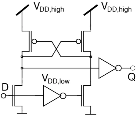
Figure 1.Asynchronous standard level converter (differential cascode voltage switch architecture)
DD,low
V
DD,low
V
DD,low
V
DD,high
V
DD,high
V clk
clk clk
clk
clk
Figure 2.Standard level converter flipflop including the asynchronous standard level shifter in the slave stage.
RN
RP
CLK4 CLK3
CLK1 CLK2
CLK
RP CLK4
CLK
CLK1 RN
CLK
CLK3
CLK
CLK CLK1
CLK3
D
Q
Figure 3. Semi-dynamic level converter flipflop in master-slave architecture. A logic decision node in the master stage is precharged during the low phase of the clock and conditionally discharged during an evaluation period triggered by the rising clock edge.
Fig. 1. Asynchronous standard level converter (differential cascode voltage switch architecture).
delay has to be long enough to not violate the flipflop hold time requirements. The time difference between the worst case propagation delay of the critical path and any other path of the circuit is called the timing slack of the respective path. The slack describes how much delay can be traded against power in the considered path. As the logic topology of most circuits is extremly interwoven, different paths cannot be op-timized independently. Anyway, it is possible to slow down short paths by increasing the transistor threshold voltage, by gate resizing or by decreasing the supply voltage. Using high threshold logic gates is beneficial especially in low activity paths where leakage currents dominate. Subthreshold cur-rent decreases exponentially with growing threshold voltage but signal propagation delay increases. The delay can be es-timated by using the well known alpha-power law [Sakurai (1990)]
td≈
VDD
(VDD−Vt h)α
, (1)
where the velocity saturation indexαhas a value between 1 and 2. Multiple-threshold logic requires additional threshold adjustment implantation during manufacturing but if avail-able the technique is very advantageous as no interface cir-cuitry between different threshold domains is required. Only a slight area penalty may occur if the minimum distance be-tween devices of different threshold voltage is mentionable increased.
Reducing the supply voltage in short paths mainly results in quadratically decreased dynamic power dissipation but also in damped leakage currents: Subthreshold current is re-duced due to Drain-Inre-duced-Barrier-Lowering (DIBL) and gate tunneling current due to the exponential dependence on the voltage drop accross the barrier. The main drawback of multi-VDDapproaches is the necessity of level converters at
the interface between the low and the high voltage domain. Book: Kleinheubacher Berichte MS No.: KH2004-A-00019
First author: Stephan Henzler 6
V
DD,high
V
DD,high
V
DD,low
D
Q
Figure 1.Asynchronous standard level converter (differential cascode voltage switch architecture)
DD,low
V
DD,low
V
DD,low
V
DD,high
V
DD,high
V clk
clk clk
clk
clk
Figure 2.Standard level converter flipflop including the asynchronous standard level shifter in the slave stage.
RN
RP
CLK4 CLK3
CLK1 CLK2
CLK
RP CLK4
CLK
CLK1 RN
CLK
CLK3
CLK
CLK CLK1
CLK3
D
Q
Figure 3.Semi-dynamic level converter flipflop in master-slave architecture. A logic decision node in the master stage is precharged during the low phase of the clock and conditionally discharged during an evaluation period triggered by the rising clock edge.
Fig. 2. Standard level converter flipflop including the asynchronous standard level shifter in the slave stage.
These circuits cause additional propagation delay in the sig-nal path and consume additiosig-nal energy. This overhead is mostly negligible if a block-level multi-VDD technique is
used with large coherent circuit blocks. However, if multi-ple supply voltages are used on gate level power and delay increments consume most of the timing slack available in the system. This means that a certain path has to be significantly shorter than the critical path to compensate for the additional delay of the level shifter circuit. Moreover the power dis-sipation within the converter has to be saved by the gates operating atVDD,lowbefore the total power dissipation can
be reduced at all. With respect to switching activity multi-VDDtechniques would be beneficual especially in data-path
logic. However, the maximum number of subsequent gates in one pipeline stage has been dramatically reduced during the last years and architectures have been highly parallelized. Hence there is a very narrow design window concerning power consumption and delay of level shifters to be used for gate-level multi-VDDtechniques. Anyway, even with
excel-lent level converters highly parallel datapath structures e.g. parallel prefix adders do not enable much power reduction. Circuits with a widespread path delay distribution are much more suitable even if the average switching activity is mostly lower.
It has been shown that an integration of the level conversion task within a flipflop can be beneficial with respect to power and delay increment. A gate level multi-VDD technique is
called clustered voltage scaling (CVS) if gates of the same supply voltage are grouped together and if the group sup-plied byVDD,lowis located directly in front of the flipflops.
Thus a VDD,high→VDD,low transition can occur anywhere
within the logic as no level converters are required. How-ever, the reverse transition is only possible in front or within the flipflops. Extended clustered voltage scaling (ECVS) al-lows theVDD,low→VDD,hightransition at arbitrary positions
St. Henzler et al.: Impact of Level-Converter on Power-Saving Capability of Clustered Voltage Scaling 313
V
DD,high
V
DD,high
V
DD,low
D
Q
Figure 1.Asynchronous standard level converter (differential cascode voltage switch architecture)
DD,low
V
DD,low
V
DD,low
V
DD,high
V
DD,high
V clk
clk clk
clk
clk
Figure 2.Standard level converter flipflop including the asynchronous standard level shifter in the slave stage.
RN
RP
CLK4 CLK3
CLK1 CLK2
CLK
RP CLK4
CLK
CLK1 RN
CLK
CLK3
CLK
CLK CLK1
CLK3
D
Q
Figure 3.Semi-dynamic level converter flipflop in master-slave architecture. A logic decision node in the master stage is precharged during the low phase of the clock and conditionally discharged during an evaluation period triggered by the rising clock edge.Fig. 3. Semi-dynamic level converter flipflop in master-slave
ar-chitecture. A logic decision node in the master stage is precharged during the low phase of the clock and conditionally discharged dur-ing an evaluation period triggered by the risdur-ing clock edge.
3 Level-Converter Circuits
The first and most common approach to level conversion is the Differential Cascode Voltage Switch (DCVS) circuit shown in Fig. 1. The input signalDout of theVDD,low
do-main is inverted by an inverter which is supplied byVDD,low.
To avoid short circuit currents the signalsDandDdrive only n-channel pull-down devices. The logic high signal at the VDD,highlevel is generated by the feedback structure. The
major drawback of this level converter circuit is the fact that both supply voltages are used within the level converter cell. As the contention between the PMOS feedback circuitry and the NMOS pull-down transistor becomes stronger with de-creasing NMOS overdrive, the delay of the circuit becomes a strong function of input voltage level. Hence a detailed characterisation of a converter standard cell becomes chal-lenging. Clustered voltage scaling performs level conversion only in front of the flip-flops. Thus the integration of level-conversion into a flip-flop circuit is straight forward. Figure 2 shows one realization of a level converter flip-flop which is based on the previously described level converter circuit of Fig. 1. As the VDD,low dependent contention is still
exis-tent in the slave the delay and power penalty of level conver-sion is a noticeable fraction of the flip-flops’s total delay and power consumption. An alternative static approach (Mah-moodi, 2002) uses a self-precharge structure to generate the high output level but still needs both supply voltages within the flip-flop cell. A semi-dynamic level converter flip-flop
Book: Kleinheubacher Berichte
MS No.: KH2004-A-00019
First author: Stephan Henzler
7
0.6 0.8 1 1.2
1 2 3 4 5
vddlow [V]
normalized propagation delay
standard level−shifter flip−flop standard levelshifter
semi dynamic level−shifter flip−flop transmissiongate−based flip−flop
Figure 4.Comparison of signal propagation delay of the level shifters in dependence of the lower supply voltage
0.7 0.8 0.9 1 1.1 1.2
0 0.5 1 1.5 2
vddlow [V]
normalized power consumption
semi dynamic level−shifter flip−flop asynchronous standard level−shifter standard level−shifter flip−flop transmissiongate−based flip−flop
Figure 5.Comparison of the power dissipation of the level shifters in dependence of the lower supply voltage
0.6 0.7 0.8 0.9 1 1.1 1.2 1.3
5 10 15 20 25 30 35
lower supply voltage [V]
pecentage of power saving
Power Reduction for C2670
no delay penalty 1 inverter delay 2 inverter delays 2.5 inverter delays
Figure 6.What-If-Scenario where the level shifter is assumed to have no power penalty but varying propagation delay. The power saving capability of the C2670 benchmark circuit vanishes rapidly with increasing converter delay.
Fig. 4. Comparison of signal propagation delay of the level shifters in dependence of the lower supply voltage.
Book: Kleinheubacher Berichte
MS No.: KH2004-A-00019
First author: Stephan Henzler
7
0.6 0.8 1 1.2 1
2 3 4 5
vddlow [V]
normalized propagation delay
standard level−shifter flip−flop standard levelshifter
semi dynamic level−shifter flip−flop transmissiongate−based flip−flop
Figure 4.Comparison of signal propagation delay of the level shifters in dependence of the lower supply voltage
0.7 0.8 0.9 1 1.1 1.2 0
0.5 1 1.5 2
vddlow [V]
normalized power consumption
semi dynamic level−shifter flip−flop asynchronous standard level−shifter standard level−shifter flip−flop transmissiongate−based flip−flop
Figure 5.Comparison of the power dissipation of the level shifters in dependence of the lower supply voltage
0.6 0.7 0.8 0.9 1 1.1 1.2 1.3 5
10 15 20 25 30 35
lower supply voltage [V]
pecentage of power saving
Power Reduction for C2670
no delay penalty 1 inverter delay 2 inverter delays 2.5 inverter delays
Figure 6.What-If-Scenario where the level shifter is assumed to have no power penalty but varying propagation delay. The power saving capability of the C2670 benchmark circuit vanishes rapidly with increasing converter delay.
Fig. 5. Comparison of the power dissipation of the level shifters in dependence of the lower supply voltage.
(Henzler, 2004) is shown in Fig. 3. It still consists of the classical master-slave structure. The master has one dynamic node which is precharged during the low phase of the clock signal. On the rising clock edge a short pulse sensitizes the evaluation path which allows an input dependent conditional discharge of the dynamic node. After the evaluation pulse feedback is activated and protects the charge on the dynamic node. Hence the circuit behaves dynamically only when the evaluation pulse is active. Afterwards the circuit is fully static again and allows robust and reliable operation even at very low frequencies.
Figure 4 shows the dependence of clock-to-Q delay on the lower supply voltage. The delay of the asynchronous level converter is relatively small at heigh values ofVDD,low
314 St. Henzler et al.: Impact of Level-Converter on Power-Saving Capability of Clustered Voltage Scaling
Book: Kleinheubacher Berichte
MS No.: KH2004-A-00019
First author: Stephan Henzler
7
0.6 0.8 1 1.2
1 2 3 4 5
vddlow [V]
normalized propagation delay
standard level−shifter flip−flop standard levelshifter
semi dynamic level−shifter flip−flop transmissiongate−based flip−flop
Figure 4.Comparison of signal propagation delay of the level shifters in dependence of the lower supply voltage
0.7 0.8 0.9 1 1.1 1.2
0 0.5 1 1.5 2
vddlow [V]
normalized power consumption
semi dynamic level−shifter flip−flop asynchronous standard level−shifter standard level−shifter flip−flop transmissiongate−based flip−flop
Figure 5.Comparison of the power dissipation of the level shifters in dependence of the lower supply voltage
0.6 0.7 0.8 0.9 1 1.1 1.2 1.3
5 10 15 20 25 30 35
lower supply voltage [V]
pecentage of power saving
Power Reduction for C2670
no delay penalty 1 inverter delay 2 inverter delays 2.5 inverter delays
Figure 6.What-If-Scenario where the level shifter is assumed to have no power penalty but varying propagation delay. The power saving capability of the C2670 benchmark circuit vanishes rapidly with increasing converter delay.
Fig. 6. What-If-Scenario where the level shifter is assumed to have no power penalty but varying propagation delay. The power saving capability of the C2670 benchmark circuit vanishes rapidly with increasing converter delay.
VDD,high is used within the semi-dynamic level converter
the delay variation with VDD,low is very small which is
beneficial for the efficiency and flexibility of multi-VDD
techniques. The standard transmission gate based flip-flop without level-conversion functionality is shown as refer-ence. Figure 5 demonstrates the dynamic power dissipation of the mentioned circuits. Dynamic power consumtion of the transmission-gate based flip-flop decreases quadratically with decreasing supply voltage. The single supply voltage and contention-free design of the semi-dynamic level con-verter keeps the power consumption constant, whereas in the classical approaches dynamic power becomes strongly de-pendent onVDD,low. This results from the contention
be-tween feedback and pull-down path which becomes stronger with vanishing overdrive of the pull-down devices. It should be mentioned that alternative asynchronous level converters with pass gate based operation principle have been proposed. As these converters are normally not integrated in flipflops they are not regarded in this context. A drawback of these converters occurs if the voltage domains change dynamically. This is not the case in CVS and ECVS but may happen in block level multi-VDDapproaches where the different blocks
can be reconfigured dynamically for changing application and performance requirements. AVDD,highlevel at the
in-put of the standard pass-gate based level converter causes a cross current from theVDD,highinput to theVDD,lowsupply.
4 Impact of Level-Converter on Total Power Reduction
The scope of this exploration is the description of the influ-ence of the level converter on the effectiveness of multi-VDD
techniques. We do not intend to optimize the assignment algorithms with respect to their slack generation capability
Book: Kleinheubacher Berichte
MS No.: KH2004-A-00019
First author: Stephan Henzler
8
0.6 0.7 0.8 0.9 1 1.1 1.2 1.3 −30
−20 −10 0 10 20 30 40
lower supply voltage [V]
pecentage of power saving
Power Reduction for C2670
no power penalty 10fJ power penalty 40fJ power penalty 60fJ power penalty
Figure 7.What-If-Scenario where the level shifter is assumed to have no propagation delay but a varying power penalty. The power saving capability vanishes rapidly with increasing power consumption in the converter.
0.6 0.7 0.8 0.9 1 1.1 1.2 1.3 0
5 10 15 20 25 30
lower supply voltage [V]
pecentage of power saving
Power Reduction for C2670 no power penalty 20fJ power penalty 20% relaxed timing constraints
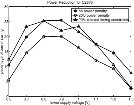
Figure 8.C2670 benchmark circuit with relaxed timing: A 20% relaxed timing specification is necessary to compensate for a20f Jpower penalty in the level converters.
1 2 3 4
0 10 20 30 40 50 60
total power saving [%]
C1355 C1908 C2670 C3540 C432 C5315 C6288 C7552 C880
Figure 9.Power saving potential of benchmark circuits: 1: semi-dynamic level converter flipflop
2: conventional level converter flipflop
3: ECVS with conventional asynchronous level converter within the logic
4: ECVS without power and delay penalty due to asynchronous level conversion (artificial)
Fig. 7. What-If-Scenario where the level shifter is assumed to have no propagation delay but a varying power penalty. The power sav-ing capability vanishes rapidly with increassav-ing power consumption in the converter.
here. Conventional design tools try to reduce dynamic power and glitching probability by a proper sizing of the gates while correct timing is assured. This procedure shifts the path de-lay distribution towards the critical path which means reduc-tion of timing slack. Hence sophisticated voltage assignment algorithms re-create this timing slack by resizing the gates again. Another approach performs these two tasks in one single design step where basic gate sizing and supply voltage assignment is done in parallel. To avoid a result dependence from a certain assignment algorithm we do not use gate re-sizing in this approach but therefore no aggressive slack con-suming power optimization in a prior step. Hence netlists with a representative path delay distribution are used. In a static timing based foreward propagation step the worst case arrival times at each node are calculated. In the following backwards processing step the worst case arrival times plus the worst case gate delays are compared to the latest possible arrival time allowed by circuit’s timing restrictions. Level converter delay and power penalty is considered if one of the succeeding gates is operated at the high supply voltage. If the remaining effective slack is positive the respective gate is assigned to the lower supply voltage. The influence on the dynamic and static power consumption is estimated by using a detailed gate characterization in combination with the state and switching probabilities of each gate.
In a first scenario the influence of level converter delay has been examined. Therefore it is assumed that the level con-verter has no power penalty. The propagation delay has been varried in multiples of an inverter delay in the consid-ered technology and with the required drive strength. Fig-ure 6 shows the relative power saving for ISCAS C2670 benchmark circuit in dependence of the lower supply volt-age. With decreasing supply voltageVDD,lowthe power
St. Henzler et al.: Impact of Level-Converter on Power-Saving Capability of Clustered Voltage Scaling 315
0.6 0.7 0.8 0.9 1 1.1 1.2 1.3
−30 −20 −10 0 10 20 30 40
lower supply voltage [V]
pecentage of power saving
Power Reduction for C2670
no power penalty 10fJ power penalty 40fJ power penalty 60fJ power penalty
Figure 7.What-If-Scenario where the level shifter is assumed to have no propagation delay but a varying power penalty. The power saving capability vanishes rapidly with increasing power consumption in the converter.
0.6 0.7 0.8 0.9 1 1.1 1.2 1.3
0 5 10 15 20 25 30
lower supply voltage [V]
pecentage of power saving
Power Reduction for C2670
no power penalty 20fJ power penalty 20% relaxed timing constraints
Figure 8.C2670 benchmark circuit with relaxed timing: A 20% relaxed timing specification is necessary to compensate for a20f Jpower penalty in the level converters.
1 2 3 4
0 10 20 30 40 50 60
total power saving [%]
C1355 C1908 C2670 C3540 C432 C5315 C6288 C7552 C880
Figure 9.Power saving potential of benchmark circuits: 1: semi-dynamic level converter flipflop
2: conventional level converter flipflop
3: ECVS with conventional asynchronous level converter within the logic
4: ECVS without power and delay penalty due to asynchronous level conversion (artificial)
Fig. 8. C2670 benchmark circuit with relaxed timing: A 20% re-laxed timing specification is necessary to compensate for a 20f J power penalty in the level converters.
As the gate delay grows in parralel, the number of gates as-signed to the lower supply voltage is reduced with decreasing VDD,low. Hence, there is a maximum power saving and an
appropriate optimum value ofVDD,low. It can be seen that
the power saving drops significantly even with small delays assumed for the level converter. Thus a fast level shifter de-sign is essential for exploiting the power saving capability of a given circuit.
Figure 7 shows the results of a second scenario where the level converter is assumed to cause only a power penalty. The power saving vanishes rapidly with increasing power con-sumption in the level shifter. WhateverVDD,low is choosen
no power will be saved at all if a power penalty of 60f F is assumed. The graph also shows the necessity for a post pro-cessing step which checks the effectiveness of each single level converter. If the power saving in the low-VDD fan-in
path of the level converter is lower than the energy overhead the converter will be removed and the respective gates con-nected toVDD,highagain. For better demonstration of power
penalty this step has been disabled to generate the graph in Fig. 7. Otherwise negative parts of the curves would be pinned to the zero percent value.
Relaxed Timing constraints can help to increase efficiency of the multiVDDscheme. Figure 8 shows that for the
demon-stration circuit a 20% relaxed timing is necessary to compen-sate for a 20f J power penalty of the level shifter. This em-phasizes the importance of low-power converter circuits for the efficiency of multi-VDDschemes.
One drawback of CVS is the fact that due to reconvergence short paths in the front part of the logic interacting with any critical path cannot be supplied by the lower supply volt-age. Extended clustered voltage scaling circumvents this drawback by allowing asynchronous level shifters at arbi-trary positions within the logic. However, asynchronous level
1 2 3 4
0 10 20 30 40 50 60
total power saving [%]
C1355 C1908 C2670 C3540 C432 C5315 C6288 C7552 C880
Fig. 9. Power saving potential of benchmark circuits: 1: semi-dynamic level converter flipflop
2: conventional level converter flipflop
3: ECVS with conventional asynchronous level converter within the logic
4: ECVS without power and delay penalty due to asynchronous level conversion (artificial).
converters are often slower and consume more power than their synchronous counterparts integrated in flipflops. Thus the power saving by reducing the voltage in these paths is usually much smaller compared to lowVDDpaths ending at
the flipflops. Figure 9 shows the maximum power saving potential of some benchmark circuits. Position 1 and 2 com-pare the results of CVS for the semi-dynamic level converter flipflop and the conventional converter flipflop. It can be seen that the fast energy efficient semi-dynamic level shifter flipflop gains considerably better results than the conven-tional approach. At position 4 the maximum power saving potential for ECVS is shown where it has been assumed that the asynchronous level converters contribute neither power nor delay penalties. Using the conventional asynchronous converter reduces the power saving significantly. In many cases almost no further reduction with respect to CVS can be observed. Following in many circuits, without effective asynchronous level converters ECVS has minor advantages over CVS. In Kulkarni (2004)] alternative asynchronous LC realizations have been discussed. However, these converters still suffer from power and delay penalties noticeable in volt-age assignment algorithms. Hence the slack in paths not end-ing directly in front of a flipflop can be used more efficiently to reduce leakage power by using high threshold devices and reduced transistor widths.
If a certain single stage gate is supplied byVDD,lowinstead
ofVDD,highthe power dissipation is reduced by
1PD =αf C
VDD,high2 −VDD,low2
+pTz · Pleak,high−Pleak,low
−pp , (2)
the input statistic is known. C describes the average load capacitance consisting of the external load plus the medium internal capacitance averaged over all transistions. The sec-ond term describes the leakage power reduction caused by the reduced supply voltage. Therefore the state probabil-ity pz=(p0...0, p0...01, . . ., p1...1)T of the input signals of the gate is multiplied by the leakage power reduction vector
Pleak,high−Pleak,low
=
Vdd,highIleak0...0(VDD,high)−Vdd,lowIleak0...0(VDD,low)
. . .
Vdd,highIleak1...1(VDD,high)−Vdd,lowIleak1...1(VDD,low)
.(3) The power penaltyppis a fraction of the total power con-sumption of the level converters distributed over allVDD,low
gates. If the respective gate is realized using high threshold devices and supplied byVDD,high the power dissipation is
reduced by
1PL=VDD,highpTz1Ileak,vt h. (4)
The vector 1Ileak,vt h
=
Vdd,highIleak0...0(Vt h,low)−Vdd,highIleak0...0(Vt h,high)
. . .
Vdd,highIleak1...1(Vt h,low)−Vdd,highIleak1...1(Vt h,high)
(5) describes the leakage power reduction due to the higher treshold voltage and can be computed by analog simulation of the gate. Equating these two power reductions yields in the switching activity
α>pTz VDD,high1Ileak,vt h− Pleak,high−Pleak,low +
pp
f C
VDD,high2 −VDD,low2
(6)
that has to be exceeded for multi-Vdd to be more effective
than multi-Vt h. Of course this estimation is only valid for
a single gate and it has been assumed that both strategies cause less delay increment than the available slack. Any-way, it supports the decision for or against multi-VDD by
decribing the influence of device properties. If the load ca-pacitance decreases e.g. by scaling or by the introduction of a low-κ dielectric in the backend the efficiency of various supply voltages decreases. A high system frequency and a widespread path delay distribution so that a very small sec-ond supply voltage can be used increases the multi-VDD
ben-efits. If leakage currents dominate the total power dissipation the use of different devices can be more beneficial than a sec-ond supply voltage: For instance a high threshold device is very beneficial in a subthreshold leakage dominated technol-ogy. However a lower supply voltage also impacts leakage currents especially if strong gate tunneling and DIBL occur. Thus the efficiency of multi-VDD not only depends on the
logic topology but also on the transistor technology. Unfor-tunately the decision between multi-VDD and multi-Vt h is
more difficult on circuit level because due to level convert-ers the decision for one gate influences the decision for other gates.
5 Conclusion
A voltage assignment tool has been applied to investi-gate the influence of signal propagation delay and power dissipation caused by level shifter circuits. Therefore “what-if-scenarios” have been used to demonstrate the effect on benchmark circuits. The power saving potential depends seriously on the the delay and power consumption of the level converters especially as timing slack is rare in many real-life circuits like datapath structures. Level converter circuits suitable for CVS have been discussed and their in-fluence on the power saving in benchmark circuits has been demonstrated. The semi-dynamic level converter flipflop enables considerably higher power saving compared to the conventional converter flipflop. In theory (no penalties) ECVS allows better results than CVS but due to the lack of fast power efficient asynchronous level shifter circuits most of the power savings is consumed in the converters. Hence we discussed the use of multi-Vt hstrategies in paths
not ending at the flipflops where efficient level conversion is possible. Anyway, the efficiency of both approaches is highly dependent on technology and circuit topology. Thus a combined scheme adapted individually to a given circuit for a given technology seems to be most beneficial.
References
Henzler, St., Koban, M., Berthold, J., Georgakos, G., and Schmitt-Landsiedel, D.: Design Aspects and Technological Scaling Lim-its of ZigZag Circuit Block Switch-Off Schemes, IFIP Interna-tional Conference on Very Large Scale Integration of System-on-Chip, 2003.
Henzler, St., Berthold, J., Georgakos, G., Schmitt-Landsiedel, D.: Single Supply Voltage High-Speed Semi-Dynamic Level-Converting Flip-Flop With Low Power And Area Consumption, PATMOS, 2004.
ITRS: International Technology Roadmap for Semiconductors, http://public.itrs.net, 2003.
Kawaguchi, H., Nose, K., and Sakurai, T. : A Super Cut-Off CMOS (SCCMOS) Scheme for 0.5-V Supply Voltage with Picoampere Stand-By Current, IEEE Journal of Solid-State Circuits, Vol. 35, No. 10, 1498–1501, 2000.
Kulkarni, S. H. and Sylvester, D.: High Performance Level Con-version for Dual VDD Design, IEEE Transactions on very large scale Integration (VLSI) Systems, 2004.
Mahmoodi-Meimand, H. and Roy, K.: Self-Precharging Flip-Flop (SPFF): A New Level Converting Flip-Flop, ESSCIRC, 2002. Meer, P. R. and Staveren, A.: New standby-current reduction
tech-nique for deep sub-micron VLSI CMOS circuits: Smart Series Switch, European Solid State Circuits Conference, 2002. Min, K., Kawaguchi, H., and Sakurai, T.: Zigzag Super Cut-off
CMOS (ZSCCMOS) Block Activation with Self-Adaptive Volt-age Level Controller: An Alternative to Clock-Gating Scheme in Leakage Dominant Era, IEEE Solid State Circuits Conference, 2003.
its Application to CMOS Inverter Delay and Other Formulas, IEEE Journal of Solid State Circuits, Vol. 25, No. 2, 1990.