30
A Low Area, Low Power 8-bit AES-CCM Authenticated
Encryption Core in 180nm CMOS Process
Dao Van Lan, Nguyen Anh Thai, Hoang Van Phuc
*Le Quy Don Technical University, 236 Hoang Quoc Viet, Hanoi, Vietnam
Abstract
This paper presents a low area, low power AES-CCM authenticated encryption IP core with silicon demonstration in 180nm standard CMOS process. The proposed AES-CCM core combines a low area 8-bit single S-box AES encryption core, improved iterative structure and other optimized circuits. The implementation results show that the proposed AES-CCM core achieves very high resource efficiency with 6.5 kgates GE and the low power consumption of 11.6 µW/MHz while meeting the requirement of the operation speed for many applications including IEEE 802.15.6 WBANs. The detail implementation and optimization results are also presented and discussed.
Received 30 March 2018, Revised 26 August 2018,Accepted28 August 2018
Keywords: AES-CCM; Authenticated Encryption; low area; low power; CMOS.
1. Introduction*
The emerging IEEE 802.15.6 wireless body area networks (WBANs) [1] tend to provide short range, wireless communications in a variety of medical and non-medical applications. Medical applications include collecting vital information of a patient continuously and forward it to a remote monitoring station for further analysis. This huge amount of data can be used to prevent the occurrence of myocardial infarction and treat various diseases such as gastrointestinal tract, cancer, asthma, and neurological disorder. WBAN can also be used
________
*
Corresponding author. Email: [email protected]
https://doi.org/10.25073/2588-1086/vnucsce.202
to support people with disabilities. For example, retina prosthesis chips can be implanted in the human eye to see at an adequate level. Non-medical applications include monitoring forgotten things, data file transfer, gaming, and social networking applications, etc. In gaming, sensors in WBAN can collect coordinates movements of different parts of the body and subsequently make the movement of a character in the game such as the moving soccer player or capturing the intensity of a ball in table tennis. The use of WBAN in social networking allows people to exchange digital profile or business card only by shaking hands.
extremely low power. Data rates, typically up to 10Mbps, can be offered to satisfy an evolutionary set of entertainment and healthcare services. Moreover, WBANs are to support a high quality of service such as the emergency messaging. Hence, it requires a strong security level for some transactions with essential information. The standard defines three levels of security. Each security level has different security properties, protection levels and frame formats. The required security level is selected during the association process, i.e., when a node is joining the network.
Advanced Encryption Standard (AES) is a highly recommended security standard for data encryption [2]. In [3], the authors also summarized some main security requirements and introduced some techniques to protect the system from possible attacks by several modes of operation such as encryption only (AES-CTR), authentication only (AES-CBC-MAC) and encrypted authentication (AES-CCM). In IEEE 802.15.6 standard for WBANs, AES-CCM is recommended for authenticated encryption (AE) purpose [1]. Hence, the low area, low power AES-CCM hardware core is highly desired. Therefore, this work focuses on the implementation of a low area, low power AES-CCM core for WBANs to provide both message encryption and message authentication.
The main contribution of this paper is that an efficient, low area, low power AES-CCM core is proposed by combining a new single S-box AES encryption core, an improved iterative structure, a simple control circuit and other optimized circuits in 180nm CMOS process. The rest of this paper is organized as follows. Section 2 presents an efficient single S-box AES encryption core architecture. Section 3 proposes the low area, low power AES-CCM core architecture and the implementation results. Finally, section 4 concludes the paper.
2. AES encryption core design
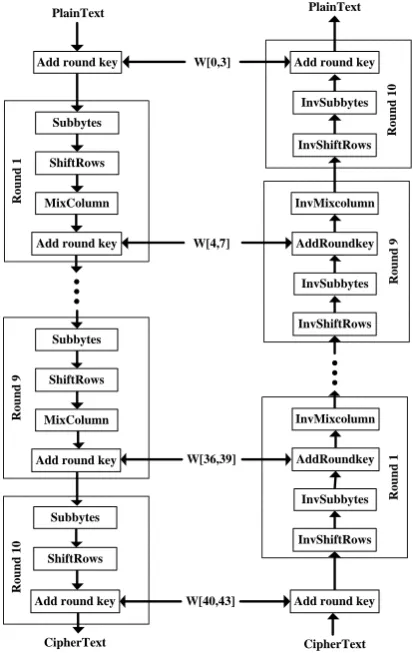
Since AES encryption block is the essential part in the AES-CCM core [2], the choice for its architecture is very important. AES encryption core processes data in 128-bit blocks with the key lengths of 128, 192 or 256 bits. In this paper, for a low area implementation, the key length of 128-bit is chosen so that an AES encryption/decryption operation requires 10 rounds. Figure 1 shows the 128-bit AES encryption/decryption algorithms. The left hand side is the encryption flow and the right hand side is the decryption one.
Although the AES algorithm has been standardized, the efficient hardware architecture and implementation methods are the topics which many researchers are focusing on.
Add round key
Subbytes
ShiftRows
MixColumn
Add round key
R
o
u
n
d
1
Subbytes
ShiftRows
MixColumn
Add round key
R
o
u
n
d
9
Subbytes
ShiftRows
Add round key
R
o
u
n
d
1
0
Add round key InvMixcolumn
AddRoundkey
InvSubbytes
InvShiftRows
R
o
u
n
d
1
InvMixcolumn
AddRoundkey
InvSubbytes
InvShiftRows
R
o
u
n
d
9
Add round key
InvSubbytes
InvShiftRows
R
o
u
n
d
1
0
W[0,3]
W[4,7]
W[36,39]
W[40,43]
CipherText CipherText
PlainText PlainText
Fig. 1. Standardized AES encryption and decryption algorithms.
the low area, low power and secure hardware implementations are highly required. Therefore, the higher power efficiency VLSI implementations are highly expected.
There are many papers in literature mentioning about AES encryption core implementation for different types of applications. For high-speed applications, AES encryption can be implemented with the round-based implementation [4], the pipeline architecture [5] or unrolled-round architecture [6]. However, these architectures lead to the high-power consumption. The largest part in the parallel architecture is the S-box. For the low-cost and low-power AES designs, the 8-bit architecture is often used since it can reduce hardware implementation area significantly. However, the throughput is reduced as well. These cores use one [7] or two S-boxes [8, 9].
Moreover, some previous works, such as [10-13], have presented the implementation of low area AES encryption cores by using the 8-bit and 32-bit datapath architectures with two optimized S-boxes. W. Zhao et al. [8] presented an efficient, low energy operation AES implementation in a standard 65nm CMOS process. However, with the fast development of many portable, wearable applications and devices, especially in IoT systems, the low area, ultra-low power and secure hardware implementations with more improvements are highly required. In the IoT era, the low power and high security hardware implementation becomes an essential issue [11].
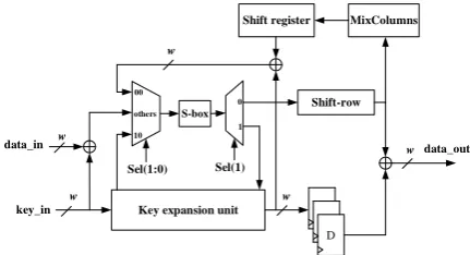
To further improve the area efficiency of the core, in this paper, the improved single S-box architecture is proposed as in Fig. 2 in which control signals are fed to the MUX (multiplexer), DEMUX and some other simple circuits. Each round is performed in 20 cycles including 16 cycles for 16 data bytes and 4 cycles for key expansion with a shared S-box using selection signal (Sel). A simple counter-based control method is applied for this architecture with a control method as presented
in Table 1 in which CNT (counter) is the value of the cycle counter register in each round and r-in is the round index ranging from 0 to 9. In the shift register and other blocks of the AES encryption core, the control signals are generated from the counter-based controller.
Table 2 presents the implementation results of the 8-bit single S-box AES core with 180nm CMOS process using Synopsys Design Compiler tool. It can be seen that the single S-box AES core can achieve very low area and power consumption with the penalty of small reduction in the operation speed.
Shift-row MixColumns
S-box
Key expansion unit key_in
data_in data_out
Shift register
D
00
10 others
0
1
Sel(1:0) Sel(1)
w
w w
w w
Fig. 2. The 8-bit AES encryption core architecture.
Table 1. Control method for the single S-box AES encryption core
r_in > 0 > 0 0
CNT 0 ÷ 15 16 ÷ 19 -
Sel(1:0) 00 10 others
Table 2. ASIC implementation results of the single S-box AES encryption core compared with
other designs
Design CMOS Technology
Area (kgates
GE)
Speed (MHz)
Power (µW/MHz)
8-bit
(This work) 180nm 2.2 46.2 8.7
8-bit
(in [6]) 180nm 2.9 50.5 34
32-bit
(in [7]) 65nm 4.4 N/A 18.9
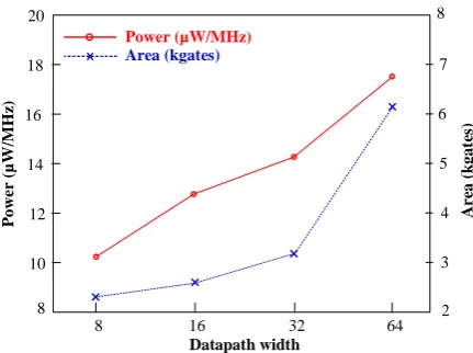
in the area and power consumption of the single S-box AES encryption core in 180nm CMOS process with different values of datapath width (w) in the hardware architecture in Fig. 2. The results are obtained from post-synthesis analysis using Synopsys Design Compiler and PrimeTime tools. In this work, to achieve low area and low power consumption, the value of w=8 for the datapath width is chosen for the ASIC implementation of the proposed AES-CCM core. In this Fig. 3, the area is estimated in the gate equivalent (GE) count of 2-input NAND gates.
3 4 5 6 7
8 10 12 14 16 18 20
A
re
a
(k
gat
es
)
P
ow
er
(
µW
/M
Hz
)
Datapath width
Area (kgates) Power (µW/MHz)
8 16 32 64
2 8
Fig. 3. ASIC implementation results of area and power consumption of the single S-box AES
encryption core in 180nm CMOS process with
different values of datapath width (w).
3. AES-CCM core design
As mentioned previously, the hardware AES-CCM design is necessary for AE operation in IEEE 802.15.6 WBANs. The existing techniques for AES-CCM implementation is mainly categorized into two groups: FPGA hardware based and software based approaches. The FPGA-based approach includes pipeline-reconfigurable AES-CCM in FPGA [14], memoryless AES-CCM [15], single-core reconfigurable AES [16] and unified data authentication encryption [17]. In [18], the software implementation of
AES-CCM requires more than 1000 clock cycles for each round with the iterative round computation of AES, which is much higher than FPGA implementation. However, there are few papers presented in literature concerned the efficient ASIC-based AES-CCM core design [19-20].
Therefore, this paper targets an efficient, low area, low power AES-CCM core for IEEE 802.15.6 WBANs. The full description of AES-CCM mechanism is presented in [2]. In this paper, we focus on the ASIC-based hardware implementation of the AES-CCM core.
With the target applications in WBANs, the proposed AES-CCM core is optimized to achieve low area and low power consumption by using 2-level iteration architecture, compact AES core and low cost finite state machine (FSM)-based controller.
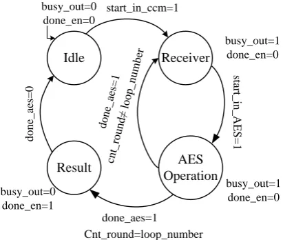
Figure 4 is the state diagram of authenticated encryption process with an iterative process. This FSM has four states including Idle,Receiver, Operation, and Result. The system has four input signals called start-in-ccm, start-in-AES, done-aes and cnt-round and the values of those signals determine what state the system will change to in the next cycle. The system changes from Idle to Receiver state as long as the input start-in-ccm is high (logic level of „1‟). If start-in-ccm is low and the system is in the Idle state, the state is not changed. If the system is in Receiver state, it changes to Operation state if start-in-AES is high. For the system, the number of loop loop-number is pre-defined, if the system is in Operation state, it changes to Result state if done-aes is high and cnt-round, which indicates the index of the current loop, equals to
loop-number. By contrast, if
encryption process is operating and does not allow any external impact, is high in Operation and Receiver states, otherwise it is „0‟. Table 3 lists the control signals generated by the FSM for the proposed AES-CCM core.
Idle
Result AES
Operation Receiver start_in_ccm=1
done_aes=1
st
ar
t_
in
_
A
E
S
=
1
cnt_ roun
d≠ lo op_
nu mb
er
d
o
n
e_
ae
s=
0
busy_out=1 done_en=0 busy_out=0
done_en=0
Cnt_round=loop_number do
ne_ aes=
1
busy_out=1 done_en=0 busy_out=0
done_en=1
Fig. 4. The state diagram of the proposed AES-CCM authenticated encryption core.
Table 3. Control signals generated by the FSM for the proposed AES-CCM core.
Round start_b start_p start_k start_m sel1 sel2
0 0 0 0 0 0 00
1÷x 0 1 1 0 1 00
x+1 0 1 1 1 1 10
x+2 1 0 1 1 0 10
(x+3)÷(2x-1) 1 1 1 0 0 01
2x 0 1 0 0 - -
Plen 128
x
The AES-CCM core architecture is shown as Fig. 5. Based on the detail AES-CCM algorithm in [2], the proposed AES-CCM core includes the 8-bit AES encryption block, key store unit (key-store), framing (B0&CTRi, payload-frames), message Integrity Code register (MIC-reg) and a simple FSM-based controller.
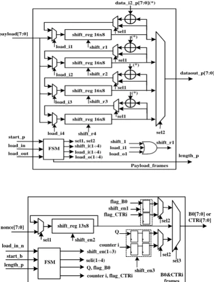
Figure 6 shows the structure of two other main building blocks in the proposed AES-CCM core as well. The payload_frames block has four 16-bit registers to reduce the hardware complexity of the proposed AES-CCM core.
The implementation results are presented in Table 4 by using Synopsys Design Complier tool and compared with other designs. It can be
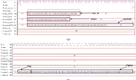
seen that the proposed AES-CCM core has the lowest area in term of equivalent gate (GE) count. This hardware resource efficiency has to tradeoff with the reduction of speed and throughput. However, the operation speed of 85.6MHz can meet the requirement of IEEE 802.15.6 WBANs [1]. Figure 7 is the chip microphotography of the proposed AES-CCM core in 180nm CMOS technology with the core circuit dimension of 340×340µm2. Figure 8 presents the post-layout simulation results with a typical test case in Synopsys VCS tool. In our simulation, the following parameters are chosen as: Klen=128, Nlen=104, Tlen=32 and Plen=256. The measurement results of the fabricated chip have also confirmed the correct operation of the proposed AES-CCM core.
4. Conclusions
In this paper, we have presented a low area, low power AES-CCM authenticated encryption core with an efficient architecture employing the single S-box AES encryption core with optimized counter-based controller, improved 2-level iterative structure and other optimized circuits. The implementation results in the ASIC hardware platform shown that with the merit of low area and low power consumption, the proposed AES-CCM core can be employed for the emerging applications including IEEE 802.15.6 WBANs. In the future, we will implement an ASIC-based sensor node for the IEEE 802.15.6 WBAN employing the proposed AES-CCM core.
Table 4. ASIC implementation results of the proposed AES-CCM core compared with others
Design In [19] In [20] This work
CMOS technology 250nm 65nm 180nm Supply voltage N/A 0.55V 1.8V Area (kgates GE) 14.9 8.1 6.5
Speed (MHz) N/A 149 85.6 Throughput (Mbps) 54 119.2 68.5 Power (µW/MHz) 440 3.98 11.6
K
8-bit AES
FSM counter
Payload_frames data
key_in[7:0]
nonce[7:0]
cipher[7:0] payload[7:0]
load_in_p
B0&CTRi frames
start_in_AES
sel1 sel1 sel1
sel4
d
o
n
e
_
a
e
s
dataout
clk, reset start_in_ccm
busy_out Key_store
load_in_n load_in_k
key[7:0] load_in_AES
MIC_reg
B0 or CTRi
Bi
data_in_xor
data_in2_p
data_in_m
data_in_m start_m
d
a
ta
_
in
2
_
p
st
a
r
t_
p start_p, start_m,start_b, start_k sel1, sel2,
sel3, sel4 sel3
length_p start_b
start_k
load_out_m
lo
a
d
_
o
u
t_
p
load_out
load_out_m, load_out_p data_in_xor
sel2
Fig. 5. Block diagram of the proposed 8-bit AES-CCM core architecture.
payload[7:0]
Payload_frames shift_reg 16x8
data_i2_p[7:0](*)
start_p
load_i1
FSM
sel1, sel2
load_i(1÷4) sel1
shift_r1
shift_i(1÷4) load_in
load_o(1÷4)
dataout_p[7:0]
length_p shift_reg 16x8
load_i2
sel1
shift_r2
shift_reg 16x8
load_i3
sel1
shift_r3
shift_reg 16x8
load_i4
sel1
shift_r4
load_out
shift_r1 load_i1
load_o1 shift_1
sel2 (*)
(*)
(*)
nonce[7:0]
load_in_n start_b
shift_en2
B0&CTRi frames shift_reg 13x8
FSM
shift_en(1÷3) seli(1÷4)
flag_B0
flag_CTRi shift_en1
B0[7:0] or CTRi[7:0]
sel2 sel3 sel2 Q
counter i
counter i, flag_CTRi Q, flag_B0 length_p
shift_en3 sel1
Fig. 6. Other building blocks of the proposed 8-bit AES-CCM core architecture.
AES-CCM Core
Fig. 7. Chip microphotography of the proposed AES-CCM core in 180nm CMOS process, the core
key_in
nonce payload
(a)
Cipher Tag
(b)
Fig. 8. Post-layout simulation results in Synopsys simulation VCS tool for the proposed 8-bit AES-CCM core: (a) Data and key inputs; (b) Cipher text and tag outputs.
Acknowledgements
This research is funded by Vietnam National Foundation for Science and Technology Development (NAFOSTED) under grant number 102.02-2015.20.
The authors would like to thank Prof. Cong-Kha Pham from The University of Electro-Communications (Tokyo, Japan), VLSI Design and Education Center (VDEC) - The University of Tokyo, ROHM CO. LTD. for the support of design tools, library, chip fabrication and Ms. Phan Thi Thanh Dung for help in the designs and experiments for this research.
References
[1] “IEEE standard for local and metropolitan area networks - Part 15.6: Wireless Body Area Networks,” IEEE Std 802.15.6, 2012.
[2] “Recommendation for Block Cipher Modes of Operation: The CCM Mode for Authentication and Confidentiality,” NIST Special Publication 800-38C, May 2004.
[3] S. Saleem, S. Ullah and K. S. Kwak, “Towards security issues and solutions in wireless body area networks,” Proc. 2010 6th International Conference on Networked Computing (INC), pp. 1-4, May 2010. [4] P. C. Liu, J. H. Hsiao, H. C. Chang, and C. Y. Lee,
“A 2.97 Gb/s DPA-resistant AES engine with self-generated random sequence,” in Proc. Eur. Solid-State Circuit Conf. (ESSCIRC), Sep. 2011, pp. 71-74.
[5] S. Mathew et al., “53 Gbps Native GF(24)2 composite-field AES-encrypt/decrypt accelerator for content-protection in 45 nm high performance microprocessors,” IEEE J. Solid-State Circuits, vol. 46, no. 4, pp. 767-776, Apr. 2011.
[6] P. Maene and I. Verbauwhede, “Single-cycle implementations of block ciphers,” in Lightweight Cryptography for Security Privacy (Lecture Notes in Computer Science), vol. 9542, T. Güneysu, G. Leander, and A. Moradi, Eds. Cham, Switzerland: Springer, 2016, pp. 131-147. [Online]. Available: https://link.springer.com/chapter/10.1007/978-3-319-29078-2-8.
[7] S. Mathew et al., “340 mV-1.1 V, 289 Gbps/W, 2090-gate nanoAES hardware accelerator with area-optimized encrypt/decrypt GF(24)2 polynomials in 22 nm tri-gate CMOS,” IEEE J. Solid-State Circuits, vol. 50, no. 4, pp. 1048-1058, Apr. 2015. [8] W. Zhao, Y. Ha, and M. Alioto, “AES architectures
demonstration in 65 nm with lowest energy per encryption,” in Proc. IEEE Int. Symp. Circuits Syst. (ISCAS), pp. 2349-2352 May 2015.
[9] A. Moradi, A. Poschmann, S. Ling, C. Paar, and H. Wang, “Pushing the Limits: A Very Compact and a Threshold Implementation of AES,” Lecture Notes in Computer Science, vol. 6632, pp. 69-88, Berlin, Germany: Springer, 2011.
[10]P. Hamalainen, T. Alho, M. Hannikainen, T.D. Hamalainen, “Design and Implementation of Low-Area and Low-Power AES Encryption Hardware Core,” Proc. 9th EUROMICRO Conference on Digital System Design: Architectures, Methods and Tools (DSD2006), pp.577-583, 2006. [11]Van-Lan Dao, Anh-Thai Nguyen, Van-Phuc Hoang
and Tuan-Anh Tran “An ASIC Implementation of Low Area AES Encryption Core for Wireless Networks,” Proc. 2015 International Conference on Comm., Management and Telecomm. (ComManTel),
pp.99-102, Dec. 2015.
[12]Van-Lan Dao, Van-Phuc Hoang, Anh-Thai Nguyen, Quy-Minh Le, “A Compact, Low Power AES Core on 180nm CMOS Process,” Proc. IEEE International Conference on IC Design and Technology (ICICDT2016), pp.1-4, Jun. 2016.
[13]D. H. Bui, D. Puschini, S. Bacles-Min, E. Beigné and X. T. Tran, “Ultra low-power and low-energy 32-bit datapath AES architecture for IoT applications,”
Proc. 2016 IEEE International Conference on IC Design and Technology (ICICDT), pp.1-4, Jun. 2016. [14]E. López-Trejo, F. Rodríguez-Henríquez, and A. Díaz-Pérez, “An FPGA Implementation of CCM Mode Using AES,” in Information Security and Cryptology-ICISC 2005., 2006, pp. 322-334
[15]K. Nguyen, L. Lanante, Y. Nagao, M. Kurosaki and H. Ochi, "Implementation of 2.6 Gbps super-high speed AES-CCM security protocol for IEEE 802.11i," 2013 13th International Symposium on Communications and Information Technologies (ISCIT), Surat Thani, 2013, pp. 669-673.
[16]I. Algredo-Badillo, C. Feregrino-Uribe, R. Cumplido, and M. MoralesSandoval, “FPGA Implementation and Performance Evaluation of AESCCM Cores for Wireless Networks,” in 2008 International Conference on Reconfigurable Computing and FPGAs, pp. 421-426, 2008.
[17]Y. Wang, J. An, and Y. Ha, “Unified Data Authenticated Encryption for Vehicular Communication,” in 2016 IEEE International Midwest Symposium on Circuits and System (MWSCAS), pp. 16-19, Abu Dhabi, UAE, Oct. 2016. [18]J. H. Yoo, “Fast software implementation of
AES-CCM on multiprocessors,” in Lecture Notes in Computer Science (including subseries Lecture Notes in Artificial Intelligence and Lecture Notes in Bioinformatics), vol. 7017 LNCS, no. PART 2, pp. 300-311, 2011.
[19]Lian Huai, Xuecheng Zou, Zhenglin Liu, Yu Han, “An Energy-Efficient AES-CCM Implementation for IEEE802.15.4 Wireless Sensor Networks,” Proc. 2009 International Conference on Networks Security, Wireless Communications and Trusted Computing, pp.394-397, Apr. 2009.
[20]Van-Phuc Hoang, Thi-Thanh-Dung Phan, Van-Lan Dao and Cong-Kha Pham, “A Compact, Ultra-Low Power AES-CCM IP Core for Wireless Body Area Networks,” IFIP/IEEE International Conference on Very Large Scale Integration (VLSI-SoC 2016), pp. 1-4, Sept. 2016.