An Improved Active-Clamped DC-DC
Converter with Modified PI Controller
B.Gamya1, Ramesh R.Halakurki2
PG scholar [PE], Department of EEE, SITAMS, Chittoor, Andhra Pradesh, India1
Professor, Department of EEE, SITAMS, Chittoor, Andhra Pradesh, India2
ABSTRACT: A new dual active-clamping dc-dc converter is proposed to obtain high efficiency. The proposed converter employs a dual active-clamping technique, while a resonant voltage doubler rectifier scheme controls the output voltage with the pulse width modulation technique. The dual active-clamping circuit serves to recycle the energy stored in the leakage inductor or the magnetizing inductor and provides zero-current turn-off switching. The voltage stresses of the main switches are clamped. The voltage transient spikes across the dual active-clamping circuit and the current stress of the current-fed side switches are limited by auxiliary dual active-clamping circuits on both sides, and zero-current switching is achieved. Also, to reduce the output voltage variation, a modified PI controller is suggested.
KEYWORDS: Converter, active-clamping, voltage doubler rectifier, high-efficiency, zero current switching (ZCS).
I. INTRODUCTION
The global demand for electrical energy has continuously increased over the last few decades. Environment and energy have become serious concerns in today’s world. Alternative sources of energy generation have drawn more and more attention in recent years. Photovoltaic (PV) sources are predicted to become the biggest contributors to electricity generation among all renewable energy generation candidates by 2040[1].The PV module need a high step-up dc-dc converter to interface the low dc voltage to the high dc voltage before making it to ac for grid-tie applications [2].A step-up dc-dc converter is needed with a high step-up ratio and high-efficiency. Among the investigated topologies, the active-clamped step-up dc-dc converters are gaining its popularity. The intention of this paper is to propose a high-efficiency dc-dc converter for the photovoltaic module integrated (PV-MIC) system [3] where a high step-up dc-dc converter and low power inverter are attached at the back of each panel.
For a power level around 250-W in the PV-MIC system applications, several high step-up dc-dc converters were proposed for the power conversion form low dc voltage to high dc voltage. The half-bridge dc–dc converter has been presented to reduce switching power losses at high-voltage side [4]. The output diodes are turned OFF at zero current by using the voltage doubler rectifier. However, an additional half-wave rectifier is needed, which increases switching power losses. Alternatively, the active-clamped dc–dc converter has been used for low-voltage PV sources [5]. It uses the active-clamping circuit and the resonant voltage doubler rectifier. However, the active-clamping circuit increases the voltage stress of power switches at low-voltage side, causing high switching power losses. Additionally, thermal management problems should be considered for a practical design of the PV MIC system.Although, the soft-switched half-bridge dc-dc converters and active-clamped dc-dc converters were proposed but they does not have a high step-up voltage conversion ratio, thus requiring a high turns ratio. High turns ratio is not favoured due to high leakage inductance at the secondary side, which causes high switching losses at the output diodes.
Vol. 3, Issue 9, September 2014
controller is suggested. The performance of the proposed converter evaluated on a 200-W PV-MIC system. A high-efficiency of 97.5%is achieved to generate 350V high output voltage from 50-V low PV module voltage.
II. CONVERTER OPERATION
Figure.1 shows the circuit diagram of proposed dc-dc converter. The step-up dc-dc converter consists of a boost type of a dual active-clamping circuit ( , , ), a transformer T, and the resonant voltage doubler rectifier ( , , , ). Also, the converter consists of main switches ( , ) and auxiliary switches ( , ) operate complementarily with a short dead time. All switches are the complementarily with a short dead time. All switches are the MOSFET’s.
( − ) Are the body diodes of switches ( − ) and ( − ) are the output capacitors of switches ( − ), respectively. The transformer T has the magnetizing inductor and leakage inductor with the turn’s ratio of 1: N, where = . is the input capacitor. is the clamping capacitor. is the output capacitor. The capacitors ,
and are large enough so that their voltages , and are considered constant, respectively. is assumed to be much smaller than . The capacitor is the resonant capacitor. Resonates with the leakage inductor .Thus, the resonant capacitor voltage is not considered constant for one switching period.
Figure.1 Circuit diagram of proposed dc-dc converter.
(a) (b) Figure.2 shows the switching waveforms of the proposed converter during one switching period . Figure.2 (a) shows
The proposed converter has six switching modes during :
Mode1 [ , ]: At = , and are turned ON. Since = , the magnetizing inductor current increases linearly as
( ) = ( ) + ( − )
(1)
At the secondary side, when is applied to the secondary winding of T. The output diode is turned ON. The series-resonant circuit consisting of and is formed. Series resonance between and , the energy stored in is transferred to . the angular resonant frequency is
= 2 f = (2)
Where is the resonant frequency. By referring to the primary side, the primary current is expressed as
( ) = ( ) + ( − ) + ( ) (3)
The output diode current is given by
( ) = sin ( − ) (4)
The resonant impedance is expressed as
= (5)
Mode 2 [ , ]: At = , the half-resonant period of the series resonance is finished. The output diode current is zero before is turned OFF. ZCS of is achieved without any reverse recovery current.
Mode3 [ , ]: At = , and are turned OFF. The primary current charges and and discharges and . and increases from zero to . and decreases from to zero. Since the switch output capacitor is very small, the time interval is considered as negligible comparing to .
Mode 4 [ , ]: At = , and are turned ON. Since =− , the magnetizing inductor current decreases linearly as
( ) = ( )− ( − ) (6)
When is reversely applied across the secondary winding of T. The output diode is turned ON. The series resonant circuit between and is formed again. By referring the output diode current to the primary side, is expressed as
( ) = ( )− ( − )− ( ) (7)
Where the output diode current is given by
( ) = ( )− sin ( − ) (8)
Mode 5 [ , ]: At t = , the half-resonant period of the series resonance is finished. The is zero before is turned OFF without any reverse recovery current.
Mode 6 [ , ]: At = , and are turned OFF. The primary current charges and and discharges and . and increase from zero to . and decrease from to zero. Since the capacitor is very small, time interval is negligible as compared to .
By the voltage-second balance relation on the magnetizing inductor , the voltages and are expressed as
= (9)
= (1− ) (10)
Vol. 3, Issue 9, September 2014
= (11)
The maximum voltage stress of and is confined to the input voltage . The voltage stress of and is confined to the clamping capacitor voltage . Figure.3 shows the relation between the clamping capacitor voltage and the duty ratio D. The dual active-clamping is used in the proposed converter. The clamping capacitor voltage in case of the dual clamping circuit is always lower than the clamping capacitor voltage in case of the conventional active-clamping circuit. It means that the switch voltage stress of the proposed converter is always lower than the switch voltage stress of previous converter [5] using the conventional active-clamping circuit. Especially, when the duty ratio is below 0.5, the clamping capacitor voltage can be lower than the input voltage . It is critically beneficial in low-voltage PV applications where more than 50% of power losses are lost as switching power losses.
Figure.3.Relation between the clamping capacitor voltage and the duty ratio D: (a) in case conventional active clamping circuit and (b) in case of the dual active clamping circuit.
III. CONTROL STRATEGY
A. A modified PI controller is to reduce output voltage variation:
The output voltage is controlled with duty ratio D. Then, the duty ratio D is represented by
= + (12)
Where is a nominal duty ratio and is a controlled duty ratio. The nominal duty ratio and the controlled duty ratio can be respectively, represented as
= 1− (13)
= ∆ (14)
Then, the duty ratio D becomes
= + = 1− + ∆ (15)
To regulate the output voltage for the output load variation, the conventional PI controller can be used for the controlled duty ratio as
= + ∫ (16)
Where ∗ is the reference output voltage, e is the voltage error between ∗and , and and are the PI control gains of the controller, respectively. The regulated output voltage is an important factor achieving high performance. The PV MIC system should provide a fast dynamic response for grid power demand in case of the distributed generation using the renewable energy sources. Where the local load power increases or decreases abruptly, the output voltage of the dc-dc converter fluctuates as the inverter load changes. It might cause grid current harmonic distortion, damaging the grid-connected power generation systems. However, because the conventional PI controller controls the output slowly, the output voltage variation exists. To reduce the output voltage variation, a modified PI controller is suggested.
The suggested controller is
= + ∫ (18)
= ( ∗− ) × 1 +| ∗ |
∝ (19)
Where is the modified error between ∗ and . ∝ is the scaling factor. The error term | ∗ |
∝ is included as
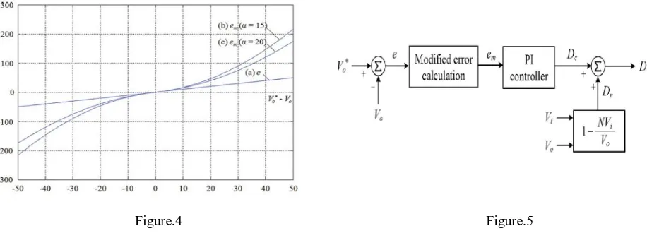
comparing to the conventional PI controller.figure.4.shows the difference between the error terms of the conventional PI controller, the error term of the suggested PI controller in case of∝= 15, and the error term of the suggested PI controller in case of∝= 20. The horizontal axis shows the difference between ∗ and . The vertical axis shows and e. Due to the term |
∗ |
∝ , a large error between ∗
and increases more than e. Thus, if the voltage error is large, the output voltage can be rapidly controlled as the suggested controller has large gain. In contrast, if the voltage error is small, the suggested controller gives almost the same characteristic as the conventional PI controller.
B. Digital implementation:
Fig. 5 shows the control block diagram of the output voltage controller. The voltage error e is calculated by comparing the reference output voltage ∗ to the measured output voltage . The modified error is generated through the modified error calculation. Then, the PI controller is used to generate the duty ratio to control the power switches. The controlled duty ratio of the voltage controller only generates the output voltage drop required to regulate the output voltage. With the addition of the nominal duty ratio to the converter, the relation between and ∆ of the converter becomes a first-order linear dynamic system with easy controllability. Thus, the addition of the nominal duty ratio relaxes the burden of the voltage controller, improving the dynamic performance.
Figure.4 Figure.5
Vol. 3, Issue 9, September 2014
IV.EXPERIMENTAL RESULTS
Figure.6. shows the primary current and switch voltages and for 200-W output power at 50-V input voltage. As shown in figure.6. and are clamped at the input voltage respectively. Figure.7 shows the primary current , clamping capacitor voltage , and switch voltages and for 200-W output power at 50-V input voltage. The clamping capacitor voltage is 48V. and are clamped at 48V.Which is even lower than the input voltage . The voltage stress of power switches is significantly reduced. Figure.8.shows the output diode voltages and and output diode currents and for output load.
Figure.6 Figure.7
Figure.6.Experimental results: primary current : 10A/ division; switch voltage : 10V/division Switch voltage : 10V/division, 10μs/division. Figure.7.Experimental results: primary current : 10A/ division; clamping capacitor voltage ; 50 V /division; switch voltage : 10V/division Switch voltage : 10V/division, 10μs/division.
Figure.8 Figure.9
Figure.8.Experimental results: Output diode voltageVDo1:10V/division; Output diode current iDo1:1A/division; Output
The proposed converter achieves the efficiency of 97.5% for 200-W output power. The previous active-clamped converter achieves the efficiency of 97.2% for 200-W output power. The efficiency of 0.3% is improved by proposed converter at 50-V input voltage for 200-W output power. The previous half-bridge converter achieves the efficiency of 97.0% for 200-W output power. Figure.10.shows the output voltage and output load current in case of the conventional and modified PI controller.
(a) (b)
Figure.10.Experimental results (output voltage : 50V/division; output load current : 0.1A/division): (a) in case of conventional PI controller, (b) in case of modified PI controller.
V.CONCLUSION
A dual active-clamping circuit with high efficiency has been proposed. Analysis, design, and simulation and experimental results for the proposed converter have also been presented. This proposed converter combines the dual active-clamping circuit and the resonant voltage doubler rectifier circuit across the power transformer with the topology proposed for soft switching dc-dc converter. The resonant voltage doubler rectifier circuit provides two resonant-current paths formed by the leakage inductance of the power transformer and the resonant capacitor. In addition, the ZCS mechanism of the switches by dual active-clamping and auxiliary switches, they reduce the switching losses and the reverse-recovery losses. The modified PI controller is suggested to reduce the output voltage variation. The proposed converter achieves a high-efficiency of 97.5% at 50-V input voltage for 200-W output power.
REFERENCES
1. Q. Li and P.Wolfs, “A review of the single phase photovoltaic module integrated converter topologies with three different DC link configurations,” IEEE Trans. Power Electron., vol. 23, no. 3, pp. 1320–1333, May 2008.
2. J. P. Lee, B. D. Min, T.J. kim, D.W. Yoo, and J.Y. Yoo, “A novel topology for photovoltaic dc/dc full-bridge converter with flat efficiency under wide PV module voltage and load range”, IEEE Transactions on Industrial Electronics, vol.55, no. 7, pp.2655-2663, Jul.2008.
3. Rodriguez and G. A. J. Amaratunga, “Long-lifetime power inverter for photovoltaic AC modules,” IEEE Trans. Ind. Electron., vol. 55, no. 7, 4. pp. 2593–2601, Jul. 2008.
5. Z. Liang, R.Guo, J.Li and A.Q.Huang, “A high-efficiency PV module-integrated DC/DC converter for PV energy harvest in FREEDM systems,” IEEE Trans. Power Electron., vol.26, no. 3, pp.897-909, Mar.2011.
6. W.Y.Choi, J. S. Yoo, and J.Y. Choi, “High efficiency dc-dc converter with high step-up gain for low PV voltage sources,” in proc. IEEE ECCE Asia, Jeju, Korea. May 30/Jun. 3, 2011, pp. 1161-1163.
7. W. Chen, W. Yao, Z. Lu, and S. Ye, “A novel ZVS active clamped asymmetrical dual switch forward dc-dc converter,” in IEEE 2009Applied Power Electronics Conference and Exposition, 2009, pp. 1061-1066.
8. D. C. Lu, and V. G. Agelidis, “ZVT interleaved boost converters with built in voltage doubler and current auto-balance characteristic” IEEE
Vol. 3, Issue 9, September 2014
BIOGRAPHY
B.GAMYA received B.Tech degree in Electrical and Electronic Engineering from Jawaharlal Nehru Technological University, Anatapur, India in 2012.Currently She is pursuing M.Tech, Power Electronics in Sreenivasa Institute of Technology and Management Studies, Chittoor, A.P, India. Her research interests are development in Power Electronics.