International Journal of Research (IJR)
e-ISSN: 2348-6848, p- ISSN: 2348-795X Volume 2, Issue 08, August 2015Available at http://internationaljournalofresearch.org
Low-Complexity Low-Latency Architecture for Identical of
Data Encoded With Hard Systematic Error-Correcting Codes
1
Piduguralla N S Prapulla &
2N.Veeraih ,
3S.Neelima
1
M.Tech (VLSI & Embedded System),
2Asst.Professor,
3
HOD, Assoc.Proffesor,
Gandhiji Institute of Science & Technology (Gist) – JNTU Kakinada Affiliated,
Gattubhimavaram (Village),Jaggayyapet (Mandal),Krishna (District),Andhra Pradesh, India.
Abstract:
In contemporary situation, circumstances in a computing system where received information needs to be compared with a piece of stored data to locate the identical entry, e.g., cache tag array lookup and translation look-aside buffer matching. Currently the consistency issues of memory are Event Upsets (EUs), which are able to invert the stored logical value in memory cells. This issue is more severe when the exaggerated memory cells are part of the configuration memory used for programming the circuit functionality. The consequences may be alterations of the circuit functionality causing errors which may only be corrected by reprogramming the device. A novel architecture for identical the data protected with an error-correcting code (ECC) is proposed in concise to decrease latency and complexity. The proposed architecture is based on the fact that the codeword of an ECC is usually represented in a systematic form consisting of the raw data and the parity information generated by encoding, and the proposed architecture parallelizes the comparison of the data and that of the parity information. To further reduce the latency and complexity, in addition, a new butterfly-formed weight accumulator (BWA) is proposed for the efficient computation of the Hamming distance. Grounded on the BWA, the proposed architecture examines whether the incoming data matches the stored data, and if not it aims to locate the erroneous bit and they are corrected. The empirical evaluation proves that the
proposed methodology discovers the best examine for consistency issues of memory.
Keywords
-
Butterfly-Formed WeightAccumulator; Translation Look-Aside Buffer; ECC; EDC; Decimal Matrix Code
I.INTRODUCTION
International Journal of Research (IJR)
e-ISSN: 2348-6848, p- ISSN: 2348-795X Volume 2, Issue 08, August 2015Available at http://internationaljournalofresearch.org
of the comparison determines the flow of the succeeding operations. When the memory array is protected by ECC, it exacerbates the criticality because of the added latency due to ECC logic. In the cache tag matching example, the cache tag directory must be accessed first. After the tag information is retrieved, it must go through ECC decoding and correction before the comparison operation can be performed. At the mean time, the corresponding data array is waiting for the comparison result to decide which way in the set to load the data from. The most recent solution for the matching problem is the direct compare method [5], which encodes the incoming data and then compares it with the retrieved data that has been encoded as well. Therefore, the method eliminates the complex decoding from the critical path. In performing the comparison, the method does not examine whether the retrieved data is exactly the same as the incoming data. Instead, it checks if the retrieved data resides in the error correctable range of the codeword corresponding to the incoming data. As the checking necessitates an additional circuit to compute the Hamming distance, i.e., the number of different bits between the two code words, the saturate adder (SA) was presented [5] as a basic building block for calculating the Hamming distance. However, it does not consider an important fact that a practical ECC codeword is usually represented in a systematic form in which the data and parity bits are completely separated from each other.
In adding, SA contributes to the increase of the entire circuit complexity as it always forces its output not to be greater than the number of detectable errors by more. In brief, we renovate the SA-based direct compare architecture to reduce the latency and hardware complexity by resolving the drawbacks. More specifically, we consider the characteristics of systematic codes in designing the proposed architecture and propose a low-complexity processing element that computes the Hamming distance faster. Therefore, the latency and the hardware complexity are decreased considerably compared with the SA based architecture.
II.
DATA
COMPARISION
METHODS
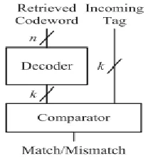
2.1 Decode-And-Compare Architecture
This illustrates the conventional decode-and-compare architecture. It reflect on a cache memory where a Kbit tag is stored in the form of an n-bit codeword after being encoded by a (n, k) code. In the decode-and compare architecture, the n-bit retrieved codeword should first be decoded to extract the original k-bit tag. The extracted k-bit tag is then compared with the k-bit tag field of an incoming address to determine whether the tags are matched or not. As the retrieved codeword should go through the decoder before being compared with the incoming tag, the critical path is too long to be employed in a practical cache system designed for high-speed access
Fig 1. Decode-And-Compare Architecture
2.2 Direct Compare Method
Direct compare method is one of the most recent solutions for the matching problem. The direct compare method encodes the incoming data and then compares it with the retrieved data that has been encoded as well .Therefore, the method eliminates the complex decoding from the critical path.
2.3 SA-Based Approach
International Journal of Research (IJR)
e-ISSN: 2348-6848, p- ISSN: 2348-795X Volume 2, Issue 08, August 2015Available at http://internationaljournalofresearch.org
complexity by resolving the aforementioned drawbacks.
III.
ADVANCED
DATA
COMPARISION METHODS
3.1 DMC Encoding
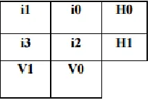
Because of high-speed caches and main memories, which are prone to soft errors, error correcting codes are used in the design and, more recently, in the design of on chip memories. For the encoding Decimal matrix code (DMC) is proposed to assure reliability in the presence of MCUs with reduced performance overheads, and a 4- bit word is encoded based on the proposed technique. First, during the encoding process, information bits i are fed to the DMC encoder, and then the horizontal redundant bits H and vertical redundant bits V are obtained from the DMC encoder. When the encoding process is completed, the obtained DMC codeword is stored in the memory. Second, the horizontal redundant bits H are produced by performing XOR operation of selected symbols per row. Third, the vertical redundant bits V are obtained by XOR operation among the bits per column.
It should be noted that both divide-symbol and arrange-matrix are implemented in logical instead of in physical. Therefore, the proposed DMC does not require changing the physical structure of the memory.
The proposed DMC scheme, for a 4-bit word is as shown in Figure.
Fig 2.4-bit DMC logical organization
In the above figure the cells from i0 to i3 are information bits. The 4-bit word has been divided into
two symbols of 2-bit.k1 = 2 and k2 = 2 have been chosen simultaneously.H0 and H1 are horizontal check bits;V0 and V1 are vertical check bits. The horizontal bits H can be obtained as follows:
For the vertical bits V, we have
The obtained parity bit is appended with the information bits so as to obtain the encoded bit.
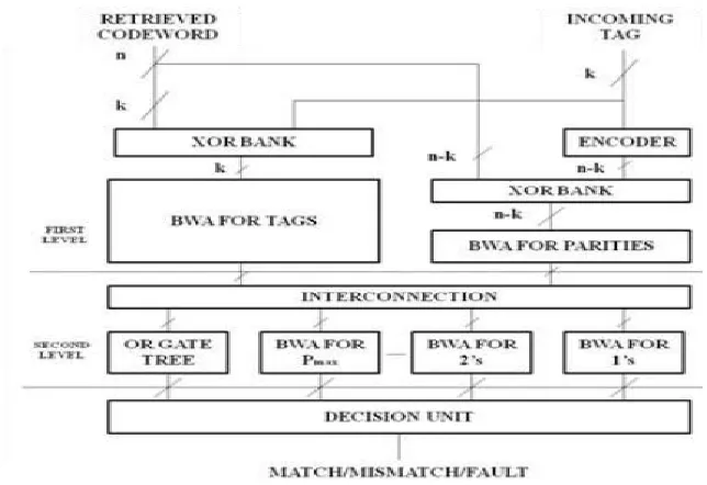
3.2 XOR Bank
XOR bank represents the array of bit-wise comparators (exclusive OR gates). It performs XOR operations for every pair of bits in X and Y so as to generate a vector representing the bitwise difference of the two codeword’s. The output from the XOR bank is then fed into BWA consisting of half adders (HAs). The numbers of 1’s are accumulated by passing the value through the BWA.
Fig 3. XOR bank structure for (8,4) code
3.3 Butterfly Formed Weight Accumulator
International Journal of Research (IJR)
e-ISSN: 2348-6848, p- ISSN: 2348-795X Volume 2, Issue 08, August 2015Available at http://internationaljournalofresearch.org
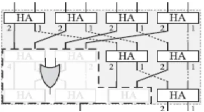
Fig4. Proposed data path design
The proposed architecture consists of multiple stages of HAs as shown in figure where each output bit of a HA is associated with a weight. The HAs in a stage are connected in a butterfly form so as to accumulate the carry bits and the sum bits of the upper stage separately. In other words, both inputs of a HA in a stage, except the first stage, are either carry bits or sum bits computed in the upper stage. This connection
method leads to a property that if an output bit of a HA is set, the number of 1’s among the bits in the paths reaching the HA is equal to the weight of the output bit.
International Journal of Research (IJR)
e-ISSN: 2348-6848, p- ISSN: 2348-795X Volume 2, Issue 08, August 2015Available at http://internationaljournalofresearch.org
In above figure for example, if the carry bit of the gray-colored HA is set, the number of 1’s among the associated input bits, i.e., A, B, C, and D, is 2. At the last stage of above figure the number of 1’s among the input bits, d, can be calculated as Since what we need is not the precise Hamming distance but the range it belongs to, it is possible to simplify the circuit. When rmax = 1, for example, two or more than two 1’s among the input bits can be regarded as the same case that falls in the fourth range. In that case, we can replace several HAs with a simple OR-gate tree as shown below. This is an advantage over the SA that resorts to the compulsory saturation.
Fig 6. Revised structure with OR-gate tree
Each XOR stage generates the bitwise difference vector for either data bits or parity bits, and the following processing elements count the number of 1’s in the vector, i.e., the Hamming distance. Each BWA at the first level is in the revised form shown in figure above, and generates an output from the OR-gate tree and several weight bits from the HA trees. In the interconnection, such outputs are fed into their associated processing elements at the second level. The output of the OR-gate tree is connected to the subsequent OR-gate tree at the second level, and the remaining weight bits are connected to the second level BWAs according to their weights. More precisely, the bits of weight w are connected to the BWA responsible for w-weight inputs. Each BWA at the second level is associated with a weight of a power of two that is less than or equal to Pmax, where Pmax is the largest power. As the weight bits associated with the fourth range are all ORed in the revised BWAs,
there is no need to deal with the powers of two that are larger than Pmax.
3.4 Error Deduction and Correction
Decimal error deduction technique is proposed and it has several advantages over the simple binary error deduction technique. The Limits of Simple Binary Error Detection can be given as follows It requires low redundant bits; its error detection capability is limited. The main reason for this is that its error detection mechanism is based on binary. The number of even bit errors cannot be detected. Can detect only a finite number of errors finite numbers of errors However, when the decimal algorithm is used to detect errors, these errors can be detected so that the decoding error can be avoided. The reason is that the operation mechanism of decimal algorithm is different from that of binary. First of all, the horizontal redundant bits H1 H0 are obtained from the original information bits. When MCUs occur in symbols, i.e., the bits in symbols are upset to “1” from “0” or vice versa. The proposed DMC can easily correct upsets of the following types
Type 1 is a single error
Type 2 is an inconsecutive error in two consecutive symbols
Type 3 is a consecutive error in two consecutive
symbols
Type 4 is an inconsecutive error in two inconsecutive
symbols
Type 5 is a consecutive error in four consecutive symbols
IV. CONCLUSION
International Journal of Research (IJR)
e-ISSN: 2348-6848, p- ISSN: 2348-795X Volume 2, Issue 08, August 2015Available at http://internationaljournalofresearch.org
protected with an ECC.To reduces the latency; the comparison of the data is parallelized with the encoding process that generates the parity information. The parallel operations are enabled based on the fact that the systematic codeword has separate fields for the data and parity. In addition, an efficient processing architecture has been presented to further minimize the latency and complexity. Consequently a sensible reduction in power is accomplished with the proposed devise.
REFERENCES
[1] J.D. Warnock, Y.H. Chan, S. M.Carey, H.Wen, P. J. Meaney, G.Gerwig, H.H.Smith, Y.H.Chan, J. Davis, P. Bunce, A.Pelella, D.Rodko, P.Patel, T.Strach, D.Malone, F. Malgioglio, J. Neves, D. L. Rude, and W. V. Huott “Circuit and physical design implementation of the microprocessor chip for the zEnterprise system,” IEEE J. Solid-State Circuits, vol. 47, no. 1, pp. 151– 163, Jan. 2012.
[2] B.Y Kong, Jihyuck Jo, Hyewon Jeong, Mina Hwang, Soyoung Cha, Bongjin Kim, and In-Cheol Park, “LowComplexity Low-Latency Architecture for Matching of Data Encoded With Hard Systematic Error-Correcting Codes,” IEEE Trans. Very Large Scale Integr.(VLSI) Syst., vol. 22, no. 7, pp. 1648 - 1652, July. 2014.
[3] H. Ando, Y. Yoshida, A. Inoue, I. Sugiyama, T. Asakawa, T. Muta, K.Morita, T. Motokurumada, S. Okada, H. Yamashita, Y. Satsukawa, A. Konmoto, R. Yamashita, and H. Sugiyama, “A 1.3 GHz fifth generation SPARC64 microprocessor,” in ISSCC. Dig. Tech. Papers, 2003, pp. 246–247.
[4] AMD Inc., Sunnyvale, CA, “Family 10h AMD Opteron™ Processor Product Data Sheet,” PID: 40036
Rev: 3.04, 2010.
Available:http://support.amd.com/us/Processor_TechD o cs/40036.pdf [Online]
[5] W.Wu, D. Somasekhar, and S.-L. Lu, “Direct compare of information coded with error-correcting
codes,” IEEE Trans. Very Large Scale Integr.(VLSI) Syst., vol. 20, no. 11, pp. 2147–2151, Nov. 2012.
[6] D. Radaelli, H. Puchner, S. Wong, and S. Daniel, “Investigation of multi-bit upsets in a 150 nm technology SRAM device,” IEEE Trans. Nucl. Sci., vol. 52, no. 6, pp. 2433–2437, Dec. 2005.
[7] E. Ibe, H. Taniguchi, Y. Yahagi, K. Shimbo, and T. Toba, “Impact of scaling on induced soft error in SRAMs from an 250 nm to a 22 nm design rule,” IEEE Trans. Electron Devices, vol. 57, no. 7, pp. 1527– 1538, Jul. 2010.
[8] S. Liu, P. Reviriego, and J. A. Maestro, “Efficient majority logic fault detection with difference-set codes for memory applications,” IEEE Trans. Very Large Scale Integr. (VLSI) Syst., vol. 20, no. 1, pp. 148–156, Jan. 2012.
[9] P. Reviriego, M. Flanagan, and J. A. Maestro, “A (64,45) triple error correction code for memory applications,” IEEE Trans. Device Mater. Rel., vol. 12, no. 1, pp. 101–106, Mar. 2012.
[10]S. Baeg, S. Wen, and R. Wong, “Interleaving distance selection with a soft error failure model,” IEEE Trans. Nucl. Sci., vol. 56, no. 4, pp. 2111–2118, Aug. 2009.
[11]G. Li, I. J. Fair, and W. A. Krzymien, “Low-density parity-check codes for space-time wireless transmission,” IEEE Trans. Wirel. Commun., vol.5, no. 2, pp. 312–322, Feb. 2006.
[12]M. Y. Hsiao “A class of optimal minimum odd-weight column SECDED codes,” IBM J. Res. Develop., vol. 14, pp. 395–301, Jul. 1970.
[13]R. W. Hamming, “Error detecting and error correcting codes,” Bell Syst. Tech. J., vol. 29, pp. 147– 160, Apr. 1950.