Comparison of Voltage Quadrupler Boost
Converter with Boost Converter
T.Vamsee Kiran1, J.Praveen2, Y.Priyanka3
Head of The Department, Dept. of EEE, DVR & Dr.HS MIC College of Technology, Andhra Pradesh,India1 Assistant Professor, Dept. of EEE, DVR & Dr.HS MIC College of Technology, Andhra Pradesh, India2 PG Student [PE&ED], Dept. of EEE, DVR & Dr.HS MIC College of Technology, Andhra Pradesh, India3
ABSTRACT:Voltage quadrupler boost converter with high-voltage transfer gain and reduced semiconductor voltage stress is proposed in this paper along with comparison of boost converter. The proposed topology apply input-parallel output-series pattern for giving a much higher voltage gain excluding implementation of very large duty cycle. The proposed converter cannot only able to achieve maximize voltage gain with lowered component count but also lessen the voltage stress of both active switches and diodes. This will allow one to choose optimum lower voltage rating MOSFETs and diodes for minimizing both switching and conduction losses. Along with, due to the charge balance of the blocking capacitor, the converter highlights spontaneous uniform current sharing characteristics of two interleaved phase for voltage boosting mode comparatively than adding an additional circuitry or complex control techniques. The quadrupler boost converter voltages, currents and efficiency at different duty ratios are presented by comparing with boost converter. Some simulation results are presented to demonstrate the effectiveness of the proposed converter.
KEYWORDS: Automatic uniform current sharing, high boost converter, low voltage stress, transformer-less, voltage quadrupler.
I.INTRODUCTION
With global energy shortage and strong environmentalmovements, renewable or clean energy sources such as solar cells and fuel cells are increasingly valued worldwide.However, due to the inherent low voltage characteristic of these sources, a high step-up dc converter is essential as a prestage of the corresponding power conditioner [1]. The conventional boostand buck–boost converters [10] , due to the degradation in the overallefficiency as the duty ratio approaches unity. Obviously cannot fulfil the application need. Besides, the extreme duty rationot only induces very large voltage spikes and increases conduction losses but also induces severe diode reverse-recoveryproblem.
Up to now many converters have been proposed to obtain maximum voltage gain. Those are dc-dc fly back converter and Phase-shifted full bridge converter etc [2]-[4]. These converters can provide large step-up voltage conversion ratios. Unfortunately, the voltage stress of diodes in those converters remains rather high and so many problems from these converters such as high voltage stress on switches, degradation in efficiency, high diode recovery problem, extra heavy circuit, etc [5]. So, in this paper, voltage quadrupler topology is proposed. It integrates two-phase interleaved boost converter to realize a high voltage gain and maintain the advantage of an automatic current sharing capability simultaneously [6]-[8].
II. OPERATING PRINCIPLE OF THE BOOST CONVERTER
This is a dc-dc power converter with an output voltage greater than its input voltage. Boost converter is known as ‘step-up chopper’. With the arrival of bipolar junction transistor (BJT) which is a self-commutated device it is used as a switch as an alternative of thyristor in dc-dc converters. It is having at least two semiconducting devices those are a diode and a transistor and at least one energy storage elements those are a capacitor, a inductor or both.
Fig1: Boost Converter
The operating principle of boost converter explained in moods. Those are ON-State and OFF-State.
ON-State: In this state the Switch S is closed. The inductor current will be raised.
OFF-State: In this state the Switch S is open. Then the inductor current flows across the diode D, capacitor C and the load R. The simulation diagram for Boost converter is shown in fig2.
The Corresponding Equations are:
Maximum Duty Cycle (D) =
V
V
out
in
*
1
min(1)
Inductor current ripple (
I
L) =L
in
f
V
s D
*
*
(min)
(2)
Inductor (L) =
V
f
I
V
V
V
out s L
in out in
)
(
(3)
Capacitor(c) =
V
f
I
out s
D
out
*
max
(4)
III. OPERATING PRINCIPLE OF THE VOLTAGE QUADRUPLER BOOST CONVERTER
The voltage quadrupler boost converter uses two more extra capacitors and two more diodes, because of that during the energy transmission time divided inductor stored energy is stored in one capacitor and another divided inductor stored energy composed by the other capacitor energy store has transferred to the output to attain much higher voltage gain. Anyway, the voltage quadrupler boost converter efficiency is higher by comparing with boost converter at different duty ratios shown in fig11. The voltage gain of voltage quadrupler boost converter is high compare to boost converter. Also, the voltage stress of both active switches and diodes are less and uses automatic uniform current sharing ability without adding extra circuitry or control methods. The detailed operating principle is explained below.
The main objective is to obtain high voltage gain and such characteristic can only be achieved when the duty cycle is greater than 0.5 and in continuous conduction mode (CCM). Only for this case , However, with duty cycle lower than 0.5 or in DCM, as there is no enough energy transfer from the inductors to the blocking capacitors, output capacitors, and load side, and consequently it is not possible to get the high voltage gain as that for duty ratio greater than 0.5. Only with duty cycle larger than 0.5, due to the charge balance of the blocking capacitor, the converter can feature the automatic current sharing characteristic that can obviate any extra current-sharing control circuit.
Fig3: voltage quadrupler boost converter
The operating principle of the voltage quadrupler boost converter can be classified into four modes. They are mode1, mode2, mode3, mode4.The current directions are also shown in figures.
Mode 1 ( ≤ < ): Switches S1 and S2 are turned ON. , , , are all OFF.
The Corresponding Equations are:
V
di
L
inL
dt
1
1 (5)
V
di
L
inL
dt
2
0
dt
C
dv
C
AA (7)
0
dt
C
dv
C
BB (8)
R
c
c
dt
C
v
v
dv
C
)
(
2 1 1 1
(9)
dt
C
dv
C
2 2R
C
C
v
v
)
(
2 1
(10)Mode 2 ( ≤ < ): For this operation mode, switch S1 remains conducting and S2 is turned OFF. Diodes and become conducting.
The Corresponding Equations are:
V
di
L
in Ldt
11 (11)
V
di
L
in Ldt
22
v
C
v
C
V
v
C
B A in
1 (12)i
i
dv
C
dt
C
C
BL
AA
2
(13)i
i
dv
C
dt
C
BC
AL
B
2
(14)R
c
c
C
dt
C
v
v
i
dv
C
A)
(
2 1 1 1
(15)
dt
C
dv
C
2 2R
C
C
v
v
)
(
2 1
(16)The Corresponding Equations are:
V
di
L
inL
dt
1
1 (17)
V
di
L
inL
dt
2
2 (18)
0
dt
C
dv
C
AA (19)
0
dt
C
dv
C
BB (20)
R
c
c
dt
C
v
v
dv
C
)
(
2 1 1
1
(21)
dt
C
dv
C
22
R
C
C
v
v
)
(
2 1
(22)
Mode 4( ≤ < ): For this operation mode, switch S2 remains conducting and S1 is turned OFF. Diodes and become conducting. The part of stored energy in inductor L1 as well as the stored energy of is now released to output capacitor C2 and load. Meanwhile, part of stored energy in inductor L1 is stored in . In this mode, the output capacitor voltage VC2 is equal to plus .
The Corresponding Equations are:
v
V
v
v
V
di
V
di
L
inL
dt
2
2 (24)
i
i
dv
C
dt
C
AC
BL
A
1
(25)i
i
dv
C
dt
C
BC
AL
B
1
(26)R
c
c
dt
C
v
v
dv
C
)
(
2 1 1
1
(27)
dt
C
dv
C
22
i
C
B
R
C
C
v
v
)
(
2 1
(28)
The voltage quadrupler boost converter is designed in such a way that, it should boost the input voltage. The converters part contains two MOSFET’s for switching action. For this MOSFET, gate pulses are given by driver circuit. The simulation diagram for quadruple boost converter is shown in fig4.
Fig4: Quadrupler boost converter simulation diagram
IV. SIMULATION RESULTS
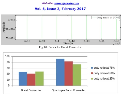
Duty Ratio Boost Converter Efficiency( ) Voltage Quadrupler Boost Converter Efficiency( )
76% 47.71 92.5
50% 40.99 83.3
25% 48.1 73.3
Table 1:-Efficiency comparison of Boost Converter and Proposed Converter for different duty ratios.
In The Fig 5, it shows the graph of time Vs voltage .The output voltage waveforms for different duty ratios of quadruple boost converter are shown in fig 5.
Fig 5: voltage waveforms of Quadruple Boost Converter for different duty ratios.
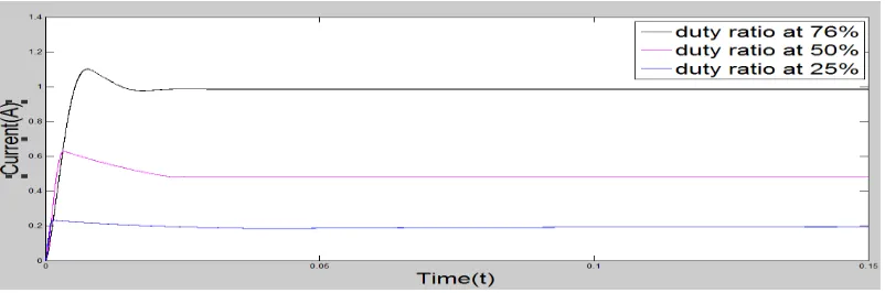
In The Fig 6, it shows the graph of time Vs current. The output current waveforms for different duty ratios of quadruple boost converter are shown in fig 6.
Fig 6: Current waveform of Quadruple Boost Converter for different duty ratios.
Fig 7: output voltage waveforms of boost converter for different duty ratio’s.
In The Fig 8, it shows the graph of time Vs current. The output current waveforms for different duty ratios of quadruple boost converter are shown in fig 8.
Fig 8: output current waveforms of boost converter for different duty ratio’s.
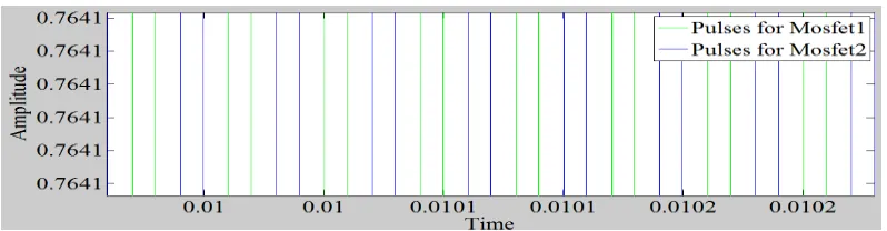
In The Fig 9, it shows the graph of time Vs amplitude. The pulses given to pulse generator of Quadruple Boost Converter is shown in fig 9.
Fig 9: pulses for Quadruple Boost Converter
.
Fig 10: Pulses for Boost Converter.
Fig: 11 Efficiency comparisons of Boost Converter and voltage quadrupler boost converter for different duty ratios
V. CONCLUSION
It can be seen that, 394V output is achieved in MAT lab simulation for 25V input. For this 0.76 duty cycle is taken. Very less voltage stress is on both diodes and active switches are gained. Main objective of this converter is to get much higher transfer gain is obtained for that low ratings of Mosfets can be used. Overall efficiency is better in designed model shown in figure 11. Conduction loss and switching losses are also made less by using lower ratings of MOSFET. No extra circuits needed to control since the use of blocking capacitor, automatic uniform current sharing of quadruple boost converter featured.
REFERENCES
[1] Ching-Tsai Pan, Chen-Feng Chuang, and Chia-Chi Chu, Member,” A Novel Transformer-less Adaptable Voltage Quadrupler DC Converter with Low Switch Voltage Stress”, IEEE TRANSACTIONS ON POWER ELECTRONICS, VOL. 29, NO. 9, SEPTEMBER 2014.
[2] R. W. Erickson and D. Maksimovic, Fundamentals of Power Electronics, 2nd ed. Norwell, MA, USA: Kluwer, 2001.
[3] L. S. Yang, T. J. Liang, and J. F. Chen, “Transformerless DC–DC converters with high step-up voltage gain,” IEEE Trans. Ind. Electron., vol. 5 56,no. 8, pp. 3144–3152, Aug. 2009.
[4] Q. Zhao and F. C. Lee, “High-efficiency, high step-up DC–Converters, IEEE Tran s. Power Electron., vol. 18, no. 1, pp. 65–73, Jan. 2003. [5] Ramakant A. Gayakwad,”Op-amps and Linear Integrated Circuit”, 4, publisher prentice Hall, 2000.
[6] M. Prudente, L. L. Pfitscher, G. Emmendoerfer, E. F. Romaneli, and R. Gules, “Voltage multiplier cells applied to non-isolated DC–DC converters,” IEEE Trans. Power Electron., vol. 23, no. 2, pp. 871–887, Mar. 2008.
[7] H. Golnabi and A. Ashrafi,” Phase‐shift generation and monitoring by a simple circuit”, Reach Gate.
[8] F. Zhang, L. Du, F. Z. Peng, and Z. Qian, “A new design method for high power high-efficiency switched-capacitor DC–DC converters,” IEEE Trans. Power Electron., vol. 23, no. 2, pp. 832–840, Mar. 2008.
[9] E.H. Ismail, M. A. Al-Saffar, A. J. Sabzali, and A. A. Fardoun, “A family of single-switch PWM converters with high step-up conversion ratio,” IEEE Trans. Circuits Syst. I, Reg. Papers, vol. 55, no. 4, pp. 1159–1171, May 2008
[10] Rajendra Meena, “Simulation Study of Boost Converter with Various Control Techniques”International Journal of Science and Research (IJSR) ISSN (Online):2319-7064
[11] Sini P. Poulose and Archana P,” A Quadrupler Voltage Interleaved DC-DC Boost Converter with Fuzzy Logic Implementation”,The
International Journal of Advanced Research in Electrical, Electronics and Instrumentation Engineering (IJAREEIE) Vol. 4, Issue 7, July 2 2015.
[12] D.Jeba Sundari Newlin , R.Ramalakshmi and S. Rajasekaran,” A Performance Comparison of Interleaved Boost Converter and Conventional Boost Converter for Renewable Energy Application’, Proceedings of 2013 International Conference on Green High Performance Computing, March 14-15, 2013.
0 20 40 60 80 100
Boost Converter Quadruple Boost Converter
duty ratio at 76%
duty ratio at 50%