University of Twente Faculty of Electrical Engineering
Chair Signals and Systems
Development of a test-bed for smart antennas, using digital
beamforming
By Taco Kluwer
M. Sc. Thesis Report no: S&S-015.01
December 2000-August 2001
Supervisors: Prof. Dr. Ir. C.H. Slump
Ir. R. Schiphorst
SUMMARY
This report describes the development of a smart antenna test-bed. The test-bed is configured as a receiver and can process the signals of a maximum of four antennas. The receiver structure is based on the heterodyne receiver concept. The heterodyne receiver is characterized by two stages. The first stage converts the received signal to an intermediate frequency, and the second stage converts this signal to the baseband.
A setup is configured to simulate the first stage by using programmable function generators. The second stage of the front-end is performed digitally. For this a quad analog-to-digital converter is used in combination with a digital signal processor. The analog-to-digital converter and the digital signal processor are editions of Texas Instruments for evaluation purposes. The digital downconversion and the beamforming tasks are defined by software.
Two algorithms are considered to be implemented; the Least Mean Square algorithm and the Constant Modulus algorithm. The Constant Modulus Algorithm is simpler to implement as it is a blind algorithm and it does not require synchronization.
The software platform is formed by a real-time operating system, which is called DSP/BIOS. The software objects that are designed, function as real-time tasks. The test-bed is designed for continuous operation. A driver for the analog-to-digital converter is implemented. The digital downconverter is implemented and tested for two channels. Extension to four channels can be done easily.
Preface
Wireless telecom has always been one of my major interests. Nowadays the telecom sector is growing fast and its behavior is dynamic, hazardous and turbulent. At the start of a 3rd generation network for mobile communications, new technologies, demands and restrictions arise. Technologies as GSM, DECT, IS95 will evolve to new standards such as UMTS. Besides these technologies Bluetooth, wireless LAN and HomeRF came up, showing many completely new insights and applications. This enormous amount of technology and its potential, ask for creative and smart solutions.
One of the developments in wireless telecom that interests me is the smart antenna. Smart antenna technology can have great effect on many important parameters in the wireless communication. Benefits to be gained are among others in the area of bandwidth, bit rates, interference rejection, power economy, and reliability. High potential indeed, and therefore smart antenna technology is at this moment a hot topic for the wireless industry. The basic idea behind smart antennas is that multiple antennas processed simultaneously allow static or dynamical spatial processing with fixed antenna topology. The pattern of the antenna in its totality is now depending partly on its geometry but even more on the processing of the signals of the antennas individually. Smart antennas enable beamforming to aim at targets or pattern modification to form the best solution for signal to noise performance or energy economy.
For my Master’s thesis I chose smart antennas as an area to focus on. I approached the chair Signals and Systems for my thesis as its research interests share a common field with my interests. During my thesis an assignment was formed and carried out. The final result of the thesis is this document containing my experiences and achievements.
I would like to thank my supervisors, Kees Slump, Roel Schiphorst and Fokke Hoeksema, for their support and advice during the Thesis. Furthermore I would like to thank Henny Kuipers and Geert-Jan Laanstra for their support on the practical work.
Table of Contents
1 Introduction ...1
1.1
Defining the assignment... 2
1.2 Overview ... 2
2 Smart
antennas
fundamentals...5
2.1 Different
approaches... 5
2.2
Smart antenna basics ... 7
2.3 Adaptive
beamforming ... 9
2.4 The
LMS
algorithm ... 10
2.5
Constant Modulus Algorithm... 13
3 Radio
frequency
front-end...15
3.1 Radio
Frequency
Transceiver ... 15
3.2 Receiver
Fundamentals... 17
3.3
Receiver building blocks ... 21
3.4
Receiver architectures in practice ... 22
3.5
RF design proposal ... 25
4 Digital receiver fundamentals ...29
4.1 Differential
detection ... 30
5.1 System
overview... 33
5.2 Hardware
implementation... 34
5.2.1 Texas Instruments TMS320C6711 development board... 35
5.2.2 THS1206 AD converter evaluation module... 36
5.3 Hardware
performance ... 37
5.4 Software
implementation... 39
5.4.1 DSP/BIOS... 39
5.4.2 Real-time analysis... 39
5.4.3 Real-time program structure ... 41
5.5 Software
design ... 42
5.5.2 Start AD conversion... 44
5.5.3 Process ping or pong... 44
5.5.4 DDCping/pong... 45
5.5.5 Beamform ... 46
5.6
Software to be implemented ... 46
6 Test
results...47
6.1 Thread
test
results... 47
6.2 Digital
downconverter ... 51
6.3 Beamform
algorithm... 52
6.3.1 Experiment 1... 53
6.3.2 Experiment 2... 56
7 Conclusions...59
8 Recommendations...61
References...63
Appendix A, Experiences with TI tools ...65
Appendix B, Matlab code ...67
Appendix C, C source code ...75
1
Introduction
In wireless telecom there is the ever-lasting search to new technologies for improvement of bandwidth, capacity, quality and so on. A lot of achievements have been made regarding modulation techniques and coding to find reliable and more efficient ways to send information wireless. One of the technologies that can contribute to the improvement of wireless systems is the smart antenna.
A smart antenna is a system in which the performance of the antenna pattern can be improved. This is done by multiple antennas, which are processed simultaneously. Dynamic changing of the antenna pattern enables the system to form a beam at a target, and with that improvement of its signal to noise ratio. The beam can also be formed to remove interference from certain directions. Spatial separation of multiple users by multiple beams enables more users per cell, as the users can re-use the frequency. These are a few examples of the use of a smart antenna system for improvement of a wireless system.
In the past a lot of effort is made to gain insight in the working of smart antenna systems. Algorithms, which enable beamforming or noise reduction have been simulated and compared with each other. Now a demand arises to see how these systems work in practice. What is possible with these systems and how well do the beamforming smart antennas perform in a real system? When using a real system, the components are not ideal and in the system design trade-offs are made to find a good working system. It is not about finding the ‘best’ system, but finding the best system under certain circumstances or constraints. A way to reveal these design parameters and gain insight in the actual system can be done by implementing a test-bed. The test-bed is a set up where the various algorithms can be tested in a real system. This thesis is carried out to design a flexible test-bed for smart antennas, to actually test smart antenna algorithms in a communication system, which explains the title of the Thesis:
1.1
Defining the assignment
To structure the work, the assignment has to be defined. A scope is first defined to form a framework to work within. The scope of the thesis is formed by the demands for the test-bed:
1. The test-bed will be based on digital beamforming 2. The test-bed will involve a real-time system
3. The test-bed will enable algorithm testing and development 4. The test-bed will be closely related to software radio 5. The test-bed will be flexible
Digital beamforming indicates the use of a digital system performing the actual beamforming function of the smart antenna test-bed by means of digital signal processing. The software radio concept is closely related with this and states that digital algorithms will also perform certain transceiver functions. A favorable choice is the use of digital signal processors. When designing a flexible system closely related to software radio a real-time system is necessary. Flexibility is required to extend the system easily and to test algorithms or transceiver functionality.
In the assignment the test-bed is considered to be a receiver. The test-bed’s functionality will be the reception, downconversion and beamforming of the incoming signals. The assignment can be formulated as followed:
“Develop a flexible smart antenna receiver that uses digital beamforming”
This definition can be split up into the following sub-definitions: 1. Research the practical issues concerned with smart antennas
2. Implement a smart antenna test-bed or setup within the framework defined above 3. Demonstrate the test-bed
Research of the practical issues is necessary, as the constraints for smart antenna receivers are different from conventional single antenna systems. A working system has to be developed, conform the defined scope. The complete setup will demonstrate a beamforming system using at least one beamforming algorithm.
1.2
Overview
Chapter 2 will discuss the fundamental aspects of the smart antenna. It includes the Least Mean Square algorithm and the Constant Modulus algorithm, which are both simple beamforming algorithms.
The concept of a digital receiver is discussed in Chapter 4. This chapter will explain the working of a digital downconverter. Besides the digital downconverter the demodulation for a (Gaussian) Minimum Shift Keying receiver (MSK) can be found in this chapter.
In Chapter 5 the implementation of the test-bed is described. The setup consists of hardware and software components, and development tools. The radio front-end’s behavior is simulated with programmable function generators.
2
Smart antennas fundamentals
This section treats the different aspects of smart antennas. A smart antenna usually involves spatial processing and adaptive filtering techniques. The field of application is very large, ranging from signal to noise improvement to the user capacity enlargement of the mobile network. A typical application will involve an adaptive algorithm to create a beam to track a user or to eliminate noise sources and therefore the smart antenna is also referred to as adaptive array or adaptive beamformer. This chapter discusses two algorithms, the Least Mean Square algorithm and the Constant Modulus algorithm.
2.1
Different approaches
The first approaches to smart antennas or adaptive arrays were made for military purposes. The aim of these investigations was the suppression of strong jamming signals in military communications. Later, the mobile industry noticed adaptive arrays as a way to reuse frequency. Nowadays there are many applications that could profit from adaptive array. Benefits can be split up in the following fields [1]:
1. Coverage; The antenna gain and the interference rejection can increase the cell coverage.
2. Capacity; Space division multiple access is a technique that enables a higher frequency reuse factor, especially when combined with a dynamic channel assignment strategy.
1. Signal Quality; The use of beamforming will result in less co-channel interference, higher gain, and with that, better signal to noise performance.
2. Access Technology; In addition to temporal multiple access techniques as FDMA, TDMA and CDMA, adaptive beamforming gives new possibilities for user detection. Equalization is less complex as the multi-path fading and delay spread is reduced.
3. Power Control; The demands for power control algorithms can be eased with the use of adaptive arrays and the use of angular information about the users. The quality of UMTS for example, depends largely on efficient power control with respect to the near-far problem and therefore it could benefit from adaptive arrays.
4. Handover; The use of angular information, and as a result of this, a better estimation of the users location can improve handover planning and execution.
6. Portable Terminal Transmit Power; If the antenna gain of the receiving base station is improved in the direction of the mobile, the transmit power of the mobile can be lowered, enabling more standby time or processing power.
It is clear that by using the adaptive array, the overall performance can be improved, giving freedom to use this improvement as a trade-off between the above-mentioned benefits. For mobile operators all of the above mentioned benefits could result in cost reduction or quality improvement. It is up to the operator to find out which benefits are important.
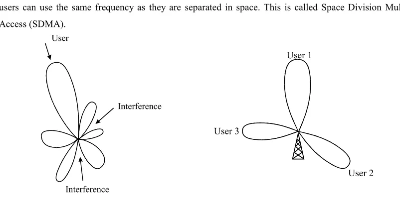
The benefits are also depending on the type of application in which the smart antenna is used. Figure 1 shows the situation of the antenna sensitivity where the signal from the user is increased and the interference is reduced by placing nulls in the direction of the interference. Another situation is represented in Figure 2, where the interference can be seen as a different user on using the same ‘frequency’ or channel. By forming patterns where the receiver for user 1, user 2 and user 3 are not interfering with each other, the users can use the same frequency as they are separated in space. This is called Space Division Multiple Access (SDMA).
Figure 1, reducing interference with adaptive beamforming
Figure 2, Space Division Multiple Access
2.2
Smart antenna basics
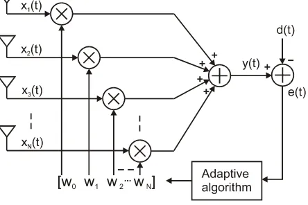
The smart antenna is basically a set of receiving antennas in a certain topology. The received signals are multiplied with a factor, adjusting phase and amplitude. Summing up the weighted signals, results in the output signal. The concept of a transmitting smart antenna is rather the same, by splitting up the signal between multiple antennas and then multiplying these signals with a factor, which adjusts the phase and amplitude. Figure 3 represents the concept of the smart antenna. The signals and weight factors are complex.
Figure 3, smart antenna concept for a receiving antenna
A linear array is shown in Figure 4. In this figure, d is the distance between the antennas and θ is the angle at which the wave front arrives.
Figure 4, linear array
This leads to the so-called array propagation vector defined by:
sin ( 1) sin
1
e
j dξ θe
j K− ξd θ T
=
v
L
(2.1)This vector contains the information of the arrival of the signal. K is the number of antenna elements used in the array and k is the index for the antenna element. The weight vector is defined by:
[
0 1 1]
T K
w
w
w
−=
w
L
(2.2)Now the array factor is defined by:
( )
( )
,
( , )
,
Ty
F
x
ξ θ
ξ θ
ξ θ
=
=
w v
(2.3)The array factor is the response of the signal arriving from angle θ; y(ξ,θ) and x(ξ,θ) are respectively the input and output of the beamforming array. If we consider ξ and d being fixed parameters of the antenna, chosen for a given frequency, combining (2.3) with (2.1) and (2.2) gives:
( )
1 sin0
K
j kd k k
F
θ
−w e
ξ θ=
=
∑
(2.4)The complex weight is defined by:
jk
k k
w
=
A e
α (2.5)Combining the array factor from (2.4) with the complex weight from (2.5) gives:
( )
1 ( sin )0
K
j kd k k
k
F
θ
−A e
ξ θ α+=
=
∑
(2.6)If a signal is arriving at the antenna array at an angle θ0, it is clear that the array response will be maximal
by adjusting the phase of the complex weight with:
0
sin
d
α
= −
ξ
θ
(2.7)Figure 5 shows the effect of an array response of a linear array with 8 antennas with the beam steered to the front at θ0 equal to zero and 45 degrees. The array response is generated by using MATLAB simulations.
-80 -60 -40 -20 0 20 40 60 80 -30
-25 -20 -15 -10 -5 0 5
array amplitude response
(d
B
)
angle(degrees)
0 degrees 45 degrees
Figure 5, beam pattern with beam steered to 0 and 45 degrees
2.3
Adaptive beamforming
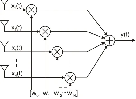
Adaptive beamforming can be done in many ways. Many algorithms exist for many applications varying in complexity. Most of the algorithms are concerned with the maximization of the signal to noise ratio. A generic adaptive beamformer is shown in Figure 6. The weight vector w is calculated using the statistics of signal x(t) arriving from the antenna array. An adaptive processor will minimize the error e between a desired signal d(t) and the array output y(t).
Figure 6, adaptive beamforming configuration
The algorithm is based on knowledge of the arriving signal. The knowledge of the received signal eliminates the need for beamforming, but the reference can also be a vector that is partly known, or correlated with the received signal. For example, the training sequence in the GSM standard, intended for channel equalization, could be used for beamforming. The rest of the signal is unknown, and beamforming using LMS can only be performed on the known training sequence.
When the adaptive algorithm is not using this knowledge, but statistic information of the signal, it is called blind beamforming. There are several algorithms for blind beamforming. For example the Constant Modulus algorithm (CMA) uses the knowledge that the modulus of the signal is constant. There are many modulation schemes where the modulus is kept constant. CMA is one of the most simple blind beamforming algorithms.
2.4
The LMS algorithm
The LMS algorithm can be considered to be the most common adaptive algorithm for continues adaptation. It uses the steepest-descent method and recursively computes and updates the weight vector. Due to the steepest-descend the updated vector will propagate to the vector which causes the least mean square error (MSE) between the beamformer output and the reference signal. The following derivation for the LMS algorithm is found in [1]. The MSE is defined by:
( )
( )
( )
22
t
d t
Ht
ε
=
∗−
w x
(2.8)d(t)* is the complex conjugate of the desired signal. The signal x(t) is the received signal from the antenna
elements, and wHx(t) is the output of the beamform antenna and (.)H is the Hermetian operator. The
expected value of both sides leads to:
( )
{
2}
{
2( )
}
2
H HE
ε
t
=
E d t
−
w r w Rw
+
(2.9)In this relation the r and R are defined by:
( ) ( )
{
}
E d t
∗t
=
r
x
(2.10)( ) ( )
{
H}
E
t
t
=
R
x
x
(2.11)R is referred to as the covariance matrix. If the gradient of the weight vector w is zero, the MSE is at its minimum. This leads to:
( )
{
}
(
E
ε
2t
)
2
2
0
∇
w
= − +
r
Rw
=
(2.12)The solution of (2.12) is called the Wiener-Hopf equation for the optimum Wiener solution:
1
opt
=
−The LMS algorithm converges to this optimum Wiener solution. The basic iteration is based on the following simple recursive relation:
(
1
)
( )
1
(
(
{ }
2)
)
2
n
+ =
n
+
µ
−∇
E
ε
w
w
(2.14)And combining (2.14) with (2.12) gives:
(
n
+ =
1
)
( )
n
+
µ
(
−
( )
n
)
w
w
r Rw
(2.15)The measurement of the gradient vector is not possible, and therefore the instantaneous estimate is used defined by (2.16) and (2.17).
( )
( ) ( )
ˆ
n
=
n
Hn
R
x
x
(2.16)( )
( ) ( )
ˆ
n
=
d n
∗n
r
x
(2.17)By rewriting (2.15) using the instantaneous estimates, the LMS algorithm can be written in its final form (2.18).
(
)
( )
( ) ( )
(
( ) ( )
)
( )
( ) ( )
ˆ
1
ˆ
ˆ
ˆ
H
n
n
n d n
n
n
n
n
n
µ
µ
ε
∗ ∗+ =
+
−
=
+
w
w
x
x
w
w
x
(2.18)One of the issues on the use of the instantaneous error is concerned with the gradient vector, which is not the true error gradient. The gradient is stochastic and therefore the estimated vector will never be the optimum solution. The steady state solution is noisy; it will fluctuate around the optimum solution. By decreasing µ the precision will improve but it will decrease the adaptation rate. An adaptive µ could solve this issue by starting with a large µ and decrease the factor when the vector converges.
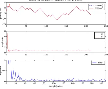
An adaptive array is simulated in MATLAB by using the LMS algorithm. When an array of 4 antennas is used, there is a maximum of 3 nulls that can eliminate the interferer. Figure 7 shows the convergence of the array for 2 interferers. The minimum error is a result of the extra ‘system’ noise that is added to all antennas. The interference signals are Gaussian white noise, zero mean with a sigma of 1. The extra system noise to all antennas is white noise with zero mean and a sigma of 0.1. The received signals are MSK signals with an oversampling of 4 and have an amplitude of 1 in the simulations.
The true array output y(t) is converging to the desired signal d(t). After 40 samples the signal is at its minimum due to the system noise. The LMS cannot filter the system noise, as it is not correlated for all four antennas. The resulting array vector has an amplitude response as shown in Figure 8.
0 50 100 150 200 250 -15 -10 -5 0 5 ph as e(ra d)
desired signal 25 degrees interferers 0 and -40 degrees
phase(d) phase(y)
0 50 100 150 200 250
0 2 4 6 8 am pl it u d e |d| |y|
0 20 40 60 80 100 120 140 160 180 200
0 0.5 1 am pl it u d e sample(index) |error|
Figure 7, LMS algorithm for an adaptive array with 4 antennas and 2 interferers.
-80 -60 -40 -20 0 20 40 60 80
-30 -25 -20 -15 -10 -5 0 5 10
amplitude response antenne pattern
(d
B
)
angle(degrees)
2.5
Constant Modulus Algorithm
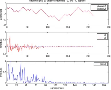
The CM algorithm is used for blind equalization of signals that have a constant modulus. The MSK signal, for example, is a signal that has the property of a constant modulus. The algorithm that updates the weight coefficients is exactly the same as for the LMS algorithm (2.18). The error is different and defined by [1]:
( )
(
( )
2)
( )
1
n
y n
y n
ε
= −
∗ (2.19)which is known as Godard’s algorithm. The CM algorithm can be found in many derived forms. The error function for a derived version is given by [19] and [20]:
( )
n
y n
( )
( )
y n
( )
y n
ε
=
−
(2.20)0 50 100 150 200 250 -15 -10 -5 0 5 pha s e (r ad )
desired signal 10 degrees interferers -10 and -40 degrees
phase(d) phase(y)
0 50 100 150 200 250
0.5 1 1.5 2 am pl it ude |d| |y|
0 20 40 60 80 100 120 140 160 180 200
0 0.5 1 am pl it u d e sample(index) |error|
Figure 9, CM algorithm for an adaptive array with 4 antennas and 2 interferers
-80 -60 -40 -20 0 20 40 60 80 -30 -25 -20 -15 -10 -5 0 5 10
amplitude response antenne, desired signal: 10 degrees, interferers: -10 and -40 degrees
(d
B
)
angle(degrees)
3
Radio frequency front-end
As there are many approaches to smart antenna implementations, it is necessary to analyze the possibilities before actually building the system. This chapter will discuss the RF front-end. In the first part the different architectures are considered. For an adaptive array there are certain aspects that need to be covered by the architecture. In general for every antenna in the array an RF front-end is necessary, performing up and downconversion and filtering. At high frequencies measurements are more subjected to feedback, noise and distortion. The length of the cables, the shape of connectors and the PCB layout are all contributing to the quality of the transceiver. Therefore the RF area can be considered a special field of work, and if it is part of a thesis a high level of expertise is required to develop a system. A way to avoid difficulties in this area would be the use of common of the shelf (COTS) transceivers. An implementation of a front-end receiver from COTS RF components appeared to be impossible, as most of the COTS components are designed for specific operation in existing communication standards or they are expensive professional products. Another way to avoid part of the design in the RF area, is to use evaluation modules from existing RF integrated circuits. The evaluation boards contain a setup with extra components and PCB board, to evaluate the product easily. The evaluation boards can also function as a reference design, for an eventual custom design.
The chapter includes a general overview of RF aspects. The chapter considers the different architectures and an evaluation is given supported by practical as well as mathematical foundations. Furthermore a proposal is made for an RF front-end for a receiver with simple components. This proposal can be used in the future as a reference for the actual design and implementation. Due to the lack of expertise in the RF field it was not possible to develop a suitable front-end.
3.1
Radio Frequency Transceiver
from fully integrated circuits for digital standards, to flexible building blocks for custom RF products. RF designing is now a special field of expertise, where a practical approach is the common way to work. It is leaded by the mobile industry and the ICs are more and more fully integrated, providing a complete receiver, transmitter or transceiver to be implemented in a mobile communication device. The mobile communication standards DECT, GSM, IS-95, D-APMS, are just a few from the pile of mobile communication technologies that exist all over the world.
In principle, a smart antenna can be formed to work with one of these technologies. Certain systems will be easier to implement and certain radio architectures are more suitable then others. From the theory in the previous chapter, it was seen that for the used algorithms complex valued signals are necessary. The receiver not only receives and recovers the in phase and quadrature signals, but also preserves phase and amplitude information of the RF signal. Figure 11 shows the representation of the receiver.
Figure 11, beamformer with radio receivers
To estimate whether a front-end is suitable for smart antenna applications, some practical issues are important. In a smart antenna system, the system consists of a set of antennas, an equal set of RF front-ends and a digital beamforming system. For a digital beamforming system the RF front-end should be designed according to the following two statements.
Phase and amplitude preservation
The receiver should be able to preserve the carriers phase and amplitude from RF to baseband. This requires the use of highly linear receivers and transmitters. An RF transceiver is a very complex device, which is subjected to non-linear operations, noise, jitter etc.
Synchronization of the radios
3.2
Receiver Fundamentals
One of the most common building blocks of a receiver is the so-called mixer. The mixer can be seen as a multiplier, which has two inputs, and one output. Generally the two inputs of the mixer are the received signal and a locally generated signal called Local Oscillator (LO). The basic function of a mixer is a translation of an input signal to a different frequency. The basic math that describes this function is formed by the trigonometric relations:
(
1) ( )
2(
(
1 2)
)
(
(
1 2)
)
1
cos
cos
cos
cos
2
t
t
t
t
ω
+
φ
ω
=
ω ω
−
+ +
φ
ω ω
+
+
φ
(3.1)(
1) ( )
2(
(
1 2)
)
(
(
1 2)
)
1
cos
sin
sin
sin
2
t
t
t
t
ω
+
φ
ω
=
ω ω
−
+ +
φ
ω ω
+
+
φ
(3.2)The angular frequencies are represented by ω1 and ω2 and the phase difference by ϕ. The function of the mixer is the translation of both frequencies to sum and difference frequencies. In receiver or transmitter architectures, only one of the two output frequencies is interesting, and therefore the mixer will be combined with an output filter, filtering either the sum or difference frequency.
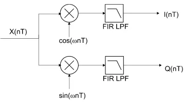
To explain the basics of the receiver, an architecture is introduced, which is mathematically the simplest form of a receiver, known as the direct-conversion receiver. The concept of the direct-conversion receiver is visible in Figure 12.
Amplifier RF BPF LO
LPF LPF
I
Q
Figure 12, Direct-conversion receiver
Consider the received signal r(t) a quadrature modulated signal represented by:
( )
I( ) cos(2
c)
Q( )sin(2
c)
r t
=
m t
π
f t
+ +
φ
m t
π
f t
+
φ
(3.3)( )
Im t
andm t
Q( )
represent respectively the in phase and quadrature message components. The received message is multiplied with the LO with exactly the same frequency:(
)
(
)
(
)
(
(
)
ˆ
)
( )
( ) cos 2
( )sin 2
cos 2
I I c Q c c
y t
=
m t
π
f t
+ +
φ
m t
π
f t
+
φ
⋅
π
f t
+
φ
(3.4)In (3.4)
y t
I( )
is the output of the receiver for the in phase message component.φ
andφ
ˆ
are respectively the phase of the received signal and the phase of the local oscillator.Using the trigonometric relations (3.4) becomes:
( )
(
)
( )
(
)
1
ˆ
1
ˆ
( )
( ) cos
( ) cos 4
2
2
1
ˆ
1
ˆ
( )sin
( )sin 4
2
2
I I I c
Q Q c
y t
m t
m t
f t
m t
m t
f t
φ φ
π
φ φ
φ φ
π
φ φ
=
− +
+ + +
− +
+ +
(3.5)
If the high frequency component is filtered out by low pass filtering and (3.5) becomes:
( )
1
( )
cos
( )
ˆ
1
( )
sin
( )
ˆ
2
2
I I Q
y t
=
m t
φ φ
− +
m t
φ φ
−
(3.6)By following the same routine to find
y t
I( )
, where the LO is phase shifted 90 degrees,y t
Q( )
is found in (3.7).( )
1
( )
cos
( )
ˆ
1
( )
sin
( )
ˆ
2
2
Q Q I
y t
=
m t
φ φ
− +
m t
φ φ
−
(3.7)When
φ
andφ
ˆ
are equaly t
I( )
andy t
Q( )
become:( )
1
2
( )
I I
y t
=
m t
(3.8)( )
1
2
( )
Q Q
y t
=
m t
(3.9)The effect of a mismatch in phase is clear from (3.6) and (3.7). If there is a mismatch between the phases, the quadrature component leaks to the in phase component and visa versa. If we consider the message as a complex vector consisting of the in phase and quadrature component, the vector is rotated by the difference in phase. This effect is important for smart antennas, as the phase component of the received signal is present in the demodulated signal.
Amplifier RF BPF LO2
LPF LPF
I
Q
LO1
IF BPF
Figure 13, heterodyne receiver
Instead of converting the received signal directly to the baseband, the first stage converts the signal to an intermediate frequency range. After this the signal is bandpass-filtered to filter one of the resulting images and after that the signal is converted to in phase and quadrature signals. The last conversion is based on exactly the same principle as the direct conversion receiver. The use of the heterodyne receiver has certain practical advantages, which are discussed in section 3.4.
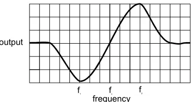
As stated before, the received signal for digital beamforming should be an I/Q signal, to represent the phase and amplitude of the incoming signals. Certain modulation types do not need an implementation where the signal is converted to the I/Q plane to finally detect the bits. For FSK a different method can be used, which is called the FM detector. Every commercial solution for an FSK receiver uses this FM detection method. The FM detector is a detector where frequency is translated to amplitude. This type of detector will in practice only work in a certain frequency range and can be regarded as the reversed version of the VCO. A typical characteristic of an FM detector is shown in Figure 15. The architecture is represented in the second stage of the heterodyne receiver structure in Figure 14.
Amplifier RF BPF
LO1
IF BPF
τ
Limiter
Tank
fc
f1 f2
frequency output
Figure 15, FM detector characteristics: input frequency vs. output amplitude
The first mixer stage remains the same as the previous heterodyne receiver, the second stage however is not using the in phase and quadrature detection but the FM detection method. The signal from the mixer is limited and after that, multiplied with a phase-shifted version of itself. The phase shift is done by an external network, which provides a phase shift depending on the frequency of the signal. After multiplying the signal, the result is filtered by a low pass network. If the incoming signal is represented by:
( )
cos 2
(
( )
)
r t
=
π
f t t
+
φ
(3.10)In (3.10) f(t) indicates the frequency modulation, where the frequency of the signal changes in time. The actual message, which is the source for the frequency modulation is left out of the formula for simplicity.
( )
cos 2
(
( )
( )
)
r t
τ=
π
f t t
+ +
φ θ
f
(3.11)The phase shift by the external network is frequency depending, which explains the phase shift θ(f). Both (3.10) and (3.11)will be multiplied in the mixer:
( ) ( )
(
( )
)
(
( )
( )
)
( )
(
)
(
( )
( )
)
cos 2
cos 2
cos
cos 4
) 2
r t r t
f t t
f t t
f
f
f t t
f
τ
π
φ
π
φ θ
θ
π
φ θ
=
+
+ +
=
+
+
+
(3.12)3.3
Receiver building blocks
The amount of different RF hardware products is very large. Often, these RF products are integrated circuits. To understand the receiver it is important to understand the separate parts of the receiver. The receiver can be split up in the following building blocks [8].
Antenna
The antenna is the interface between the receiver and the free air. The antenna has many characteristics as gain, bandwidth, radiation efficiency, beam width, and beam efficiency. The antenna is the interface between air and receiver and therefore the signals must be transferred as good as possible. The antenna should be impedance matched between the free air and the receiver input.
Low-noise amplifier
The low-noise amplifier (LNA) is the first amplifier in the receiver chain. Its influence on the noise figure is strong compared to the subsequent amplifiers. The amplifier must have a high gain and a very low noise figure. Too much gain compresses amplifiers in the rest of the circuit. A tradeoff must be made between gain and noise figure.
RF filters
The RF filter is necessary to filter the desired signal from out-of-band noise. Especially the so-called image frequency, which has the same frequency difference to the LO as the desired signal, can distort the signal. This way only the desired signal is transferred to the IF frequency.
Mixer
The mixer is a circuit, which is injected with the received signal and a reference signal from an oscillator. The mixer converts the desired frequencies to the IF band. This requires the need for an RF filter as stated before. A special type of mixer is the image reject mixer, which eliminates the image band in the mixer itself. This type of mixer is not discussed in this thesis.
Local Oscillator
IF filter
Only the IF frequency range is passed by the IF filter. The summed result of the LO and the carrier frequency is removed as well as out of band noise.
Detector
The final stage is a detector to convert the signal to a suitable baseband signal. The type of detector is depending on the modulation technique used. For FSK an FM detector is used, which converts the frequency shifted signal to an analog NRZ signal. The I/Q demodulator is necessary if a form of quadrature modulation is used.
3.4
Receiver architectures in practice
The direct-conversion receiver structure is simple in theory but difficult to realize in practice. Certain problems make the realization of this structure nearly impossible [14]. The first problem is the leakage from the local oscillator to the antenna port. As the LO has exactly the same frequency as the carrier signal, this received signal is indistinguishable from the transmitted signal from other systems in the vicinity. At higher frequencies, more problems arise, due to the effect of devices and circuits which act as antennas. Very small interconnects can become an antenna in the gigahertz frequency range.
The second problem is the leakage from the RF port to the LO’s VCO. This effect only occurs at strong signals, which can pull of the VCO’s frequency. Small phase shifts will induce the shifting of the VCO’s frequency, with strong effects on phase-modulated systems. Therefore the problem is less present then the leakage from the oscillator to the RF port, but still degrading the performance of the receiver.
The heterodyne receiver concept is not suffering from the above problems as the LO is not the same as the carrier. The heterodyne receiver is widely used in al types of receivers from mobile terminals to FM radio receivers. The heterodyne receiver has improved a lot in the last years because of new technologies. RLC filters, ceramics, quartz crystals and surface acoustic wave devices have resulted in a high quality receiver structure. However, due to these costly extra devices in the heterodyne receiver, the direct conversion receiver is gaining popularity again and special on-chip architectures compensate for the previous described problems.
PCB lines suddenly become small antennas that pick up noise and introduce distortion and feedback. Although the current SMD components are very small they are large enough to be sensitive to these effects. The filters generally consist of the following types:
- Surface Acoustic Wave filter (SAW) - RLC filter
- RC filter
The SAW filter is one of the most common RF filter nowadays and it is actually one component. The advantage is that they are available in a wide range of frequencies or bandwidths. They are characterized by a sharp cut-off, hence being very frequency selective. The disadvantage is that they are ceramic and therefore very expensive. Furthermore SAW filters suffer from high insertion losses. Besides RF filters the SAW filter is also used as IF filter when the frequency is relatively high. The output of a local oscillator can be filtered also to eliminate noise.
The RLC filters are common types for IF filters and consist of a resistance, inductance and capacitance. They can be formed in many ways and different orders. RLC filters involve multiple components and they are therefore subjected to noise and feedback. If the IF frequency is low, even a low-pass RC filter can be used. Low pass filters are also common to filter outputs of the detector.
The implementations of different systems range from application-specific single-chip solutions, to custom configured solutions with multiple chips. Figure 16 shows a multi-chip transceiver configuration for a dual band phone.
The example combines three chips to for a dual band phone for CDMA and AMPS. Both are using the same IF frequency reducing the need for different designed filters and different local oscillators. Furthermore it is clear that the system uses two stages for the up and down conversion and the baseband signals are I/Q signals. The implementation requires a lot of hardware outside the chip, which should be designed carefully. The RF hardware from chip to antenna and the high frequency filters, combined with the PCB layout are most critical.
Figure 17, single-chip DECT transceiver design example [21]
Figure 17 shows a DECT transceiver implementation with only one chip. For the downconversion two stages are used. The first filter is a bandpass filter for image rejection, the second is a SAW filter for IF filtering and the third is an LC filter for the IF signals. The system uses an FM detector which needs another off-chip filter, known as an RLC tank. The RLC tank is a network that provides the frequency depending phase shift, for the FM detector. Details on the FM detector can be found in section 3.2 For the upconversion a VCO is used with a PLL. The upconversion in DECT is less critical as it is a special form of FSK, and can therefor be done with one stage in the form of a VCO.
Both the single and multi-chip transceiver systems show the diversity of hardware, which can be used to implement receiver and transmitter functionality. When custom designs are necessary, multi-chip is a solution, when a standard communication system is needed most of the dedicated single chips will satisfy.
System Frequency description
DECT 1.800-1.900 (GHz)
DECT is a standard for personal cellular systems. The DECT system is for indoor telephone and data systems. ISM 2.400-2.483
(GHz)
The ISM (Industrial, Scientific, Medical) band for indoor applications. The transmit power is limited. The band will be occupied with hiperlan and bluetooth devices
ISM 868 (MHz) Another ISM band
Table 1 , bands suitable for experiments
It should be able to do experiments in the DECT band without disturbing too much other DECT systems. The range of a DECT system is limited and the number of channels is quite high. When there is not a data DECT system in the area, which can use multiple systems, but only phone systems, the chance is limited that the disturbance of one channel would be a problem.
The 2.4GHz ISM band is one of the most interesting bands, as the ISM band is totally free to use. The wide bandwidth is interesting as well, it give a lot of space for the hardware to operate in.
The lower ISM is another option. Though quite narrow, the frequency is low, easing the constraint for the hardware. However a larger wavelength will require larger antennas and a larger array, which can be a disadvantage.
3.5
RF design proposal
Due to the lack of experience in the field of RF design, the actual implementation of an RF frontend was not possible in this thesis. An effort has been made to design the RF front-end for a beamforming system and the result is a general RF design proposal. The design can be regarded as a high level reference design, which fulfills the demands for a beamforming network. Before starting with the design, the following guidelines are followed to form the design proposal:
The building blocks will be non-single chip solutions
The building blocks are available in the form of evaluation modules
To be partly depending on the actual implementation issues concerned with RF design a evaluation module is a good starting point for understanding and experimenting with the RF hardware. Most of the evaluation modules are properly designed PCB’s with impedance matched inputs and outputs. A disadvantage could be the fact that the combining of multiple evaluation modules involves signals traveling over long distances when the evaluation modules are connected to each other.
The receiver will be able to preserve phase and amplitude information
This was also stated in the beginning of this chapter. The downconversion method must be able to preserve the phase and amplitude of the signal. Most of the time the so-called mixers are sufficient for this function.
The receiver elements can be synchronized
To be sure that the total receiver is not suffering from independent phase drift for the different radios, it is important that the receiver modules or building blocks can be synchronized in a way. This normally involves synchronization of the LOs, or the use of one LO for different radio-chips.
IF sampling is used, which eliminates the use of a frequency detector
IF sampling involves the conversion of IF frequencies to the digital domain. This means that the second analog stage in a receiver is not required anymore, which eliminates the use of analogue filters and another local oscillator. The usage of IF sampling involves fast AD converters which can sample the rather high IF frequencies. As the current AD converters are very fast ranging up to one gigasamples per second, the IF frequency is not so much of a problem. The digital hardware following the AD converters to perform downconversion and demodulation could be a problem, as the total throughput is subjected to the processors limited memory bandwidth and processing power. In that case, additional hardware is necessary to fulfill digital downconversion using for example an FPGA or ASIC digital downconverter.
Figure 18, design concept with MAX2411A
4
Digital receiver fundamentals
This chapter will describe the properties of a digital receiver. The digital receiver is part of the test-bed in the form of a digital downconverter. The sampled input signal is downconverted digitally to an in phase and quadrature stream. The type of modulation that is selected is minimum shift keying (MSK) or if desired Gaussian minimum shift keying (GMSK). Furthermore the signal needs to be demodulated. The signal is converted from the I/Q signals to an actual bit sequence.
Instead of performing the conversion from radio frequency to the baseband using analogue integrated circuits, it is possible to do the conversion partly analogue and partly digital. The current state-of-the-art digital hardware is able to process digital signals up to one gigahertz. For certain receivers an all-digital approach is possible. In that case, the antenna output is amplified, and sampled by a high speed AD converter. Digital algorithms perform the complete transformation from the RF domain to the baseband. When the digital hardware is less powerful, the RF frequency might be too high to be sampled and processed. It is possible to sample the analogue signals after downconversion to the IF. The translation of the IF domain to the baseband can than be done in digital hardware. This is called IF sampling, also know as a form of direct sampling. The digital downconversion can be done by configurable hardware or by software on a general-purpose processor. This functional unit, which performs the downconversion, is called a digital downconverter (DDC). For digital communications, the generalized digital receiver is comparable to the analogue version. Instead of using an analogue multiplier and a local oscillator, the software or digital hardware fulfils these functions.
Figure 19, generalized digital receiver
When the IF frequency is one fourth of the sample frequency, both the digital oscillators are reduced to a repeating vector of [1 0 –1 0] for the ‘cosine’ oscillator and [0 1 0 –1] for the ‘sine’ oscillator. The digital multiplier can perform multiplication at an even lower rate, as half of the numbers to multiply with is zero. This is interesting as it reduces the load on the processor, or it simplifies the architecture for a digital downconverter. A FIR filter is sufficient to filter the output of the multipliers to remove the summed component. The result is that the input signal is converted to a baseband signal.
4.1
Differential detection
To implement an MSK receiver on a DSP, several functional blocks are necessary. If the I and Q signals are available, the receiver can be build using a differential detector, a frequency compensation loop, and a bit clock recovery loop, followed by hard decision as represented in Figure 20.
Figure 20, digital receiver with frequency compensation and bit-clock recovery
The differential detector is a simple one bit differential detector, which compares the quadrature component with the in-phase component and visa versa. The choice for a differential detector is following from the fact that MSK modulation involves the phase shift of ½πor -½π. The differential detector is described by [17]:
(
)
n n n N
s
z z
∗−
= ℑ
⋅
(4.1)sn is the output of the differential detector, zn is the nth sample representing the complex input vector. zn-N
The value of N is Tb/Ts, where Tb is the bit period and Ts is the sampling period. Value N is an integer, but
normally the actual transmitter and receiver clocks are never exactly synchronized. The receiver might have a sampling clock that is a little bit off. In this case, the digital downconverter will have a frequency offset too as its frequency is coupled to the sampling frequency. A large frequency mismatch will cause the signals to drift in the I/Q plane. This drift can be corrected by a digital frequency compensation loop. An interesting approach is made in [17]. Frequency recovery is necessary for a large frequency mismatch, for example a quarter of the bit rate. This large frequency offset is regularly caused by a Doppler shift.
As N is not truly an integer in many cases, the best instant with the lowest ISI must be selected. An adaptive timing algorithm corrects the sampling instant. Assuming that the frequency mismatch is low, the frequency compensation loop can be removed from the digital receiver in Figure 20. The differential detector’s clock is only a little off in that case. The signals in the I/Q plane may drift, but the differential signals will only be shifted by a fixed fraction.
4.2
Bit clock recovery
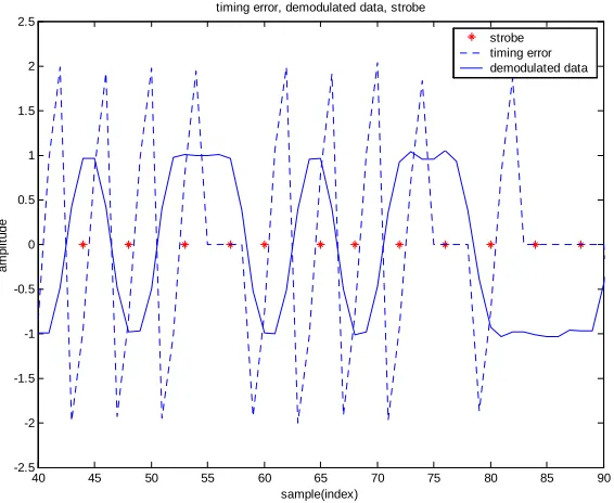
To detect the bits from the signal that is received from a differential detector, the optimum sample instant must be detected. This is the point with the least amount of inter symbol interference (ISI). Normally a correlator finds the beginning of a frame and recovers the first bit. The optimum sample instant of the next bit is then step N ahead. Due to the mismatch between the transmitter and receiver, which means that the next bit is not exactly N steps ahead from the last detected bit. It will be a fraction less or a fraction more then N. This means that the strobe, which indicates the best sampling instant, needs to be corrected, when the timing error for the bit clock is more then half of the sampling time. For this an error function can be used. The error function is given by [17]:
( )/ 2
(
sgn
( )
sgn
(
)
)
n n N n n N
e
=
s
−⋅
s
−
s
− (4.2)40 45 50 55 60 65 70 75 80 85 90 -2.5
-2 -1.5 -1 -0.5 0 0.5 1 1.5 2 2.5
sample(index)
a
m
p
lit
u
d
e
timing error, demodulated data, strobe
strobe timing error demodulated data
Figure 21, timing error and the recovered strobe
The instant on which the bit is estimated is called the strobe instant. This value of the strobe instant is an index of a sample in the demodulated data. The strobe estimation algorithm is given by:
(
1)
1 k
k k strobe N
strobe
strobe
N round
λ
e
−
− +
=
+ −
(4.3)The current strobe instant is based on the previous strobe, the timing error, N and λ. The selected timing error is the timing error for the sample with index: ‘previous strobe’ plus N. strobe0 is generally found by a
correlator that finds the start of the bit sequence. A good choice for λ is 0.5. When the absolute timing error is higher then 1, the strobe will be advanced or slowed down by one. The maximum error is 2 and the threshold of 1 is intuitively correct. Figure 21 shows the result of the strobe estimation algorithm. The bit sequence is now recovered by using:
(
)
sgn
k k strobe
m
=
s
(4.4)mkis the demodulated message based on a NRZ bit sequence, consisting of the ‘signed’ samples with index
5
The test-bed: implementation
This chapter discusses the implementation of the test-bed. The implementation is based on the reference design in the Chapter 3. First the general system is given. After the system overview, the hardware will be discussed as well as its performance. In the last part the software design on task level is treated. The performance of the software will be discussed in Chapter 6.
5.1
System overview
The system will be build following the heterodyne receiver concept, which is shown in Figure 22. The RF part consists of one mixer stage. The mixers are synchronized with one local oscillator and the output IF signal is filtered to reject images and to reduce noise. The IF signal is then sampled, and the digital downconverters convert the signal to in-phase and quadrature baseband signals. Beamforming is performed digitally.
Digital Beam-former
I
Q I
Q I
Q
I
Q A
D
A D
A D A
D
Figure 22, basic concept of the smart antenna receiver
The AD converters in Figure 22 are implemented by a quad channel AD converter of Texas Instruments, the THS1206. The digital downconverter and beamform algorithm can be implemented in software, running on an evaluation module for the Texas instruments TMS320C6711. Both the selected AD converter and the DSP board are compatible with each other. The configuration is visible in Figure 23.
Figure 23, set-up of the test-bed
The working of the system is as followed. All inputs are sampled by the sample and hold units simultaneously. A multiplexer feeds the signals to the AD converter sequentially. The AD converter fills its FIFO until the buffer is almost full, depending on its speed and configuration. At 8 or 12 samples in the FIFO it will indicate to the EDMA controller that it is ready to send over the data. This is done by using an external interrupt. The EDMA controller is triggered by the external interrupt and it will copy the data from the AD converter’s FIFO to an assigned memory block (large buffer). When this large buffer is full, the EDMA controller generates an interrupt, which indicates that the data in the buffer is ready to be processed by the digital signal processing algorithms. This EDMA controller takes the data acquisition load completely to reduce processor usage. The processing power is now available for the digital downconversion and the beamforming algorithm.
The programmable function generators (HP 33120A) can be programmed with a range of 16000 values between +2047 and –2047. The signal type that is chosen as modulation type is minimum shift keying (MSK) or, if desired, Gaussian minimum shift keying (GMSK). The sample frequency is 4 times the IF frequency to be sure that downconversion can be done as in Chapter 4. The system uses digital beamforming based on the LMS or CM algorithm. Details on these algorithms can be found in Chapter 2.
5.2
Hardware implementation
for software-defined radio with or without beamforming. For simplified communication systems and custom defined radio systems, the system is satisfying. The next sections discuss the details on the hardware. The performance of the hardware is found in section 5.3.
5.2.1
Texas Instruments TMS320C6711 development board
The development board has the following facilities:
• 150MHz TI floating-point DSP
• 16 Mb RAM
• onboard AD/DA converter
• parallel port interface
• emulation JTAG controller
• 2 line I/O
• EVM compatible Daughtercard Interface
• 128K Flash ROM
The C6711 processor can be split into three parts, the CPU core, the peripherals and the memory. Eight functional units operate in parallel split up into two equal sets. This is because of the dual data path that is available in the processor. These units use two register files of 16 32-bit registers. Figure 24 shows the block diagram for the CPU.
Algorithms that need to be executed fast must be optimized for the functional units and its data paths. The optimization can be done by hand in assembly, or partly in C by the compiler. The compilers ability to optimize code is limited and the result is normally not as good as when optimizing assembly by hand. A way to build C code, called ‘software pipelining’, enables the compiler to optimize the code more easily [29]. The functional units are split up in two multipliers and six ALUs. There is no dependency check in the processor, which means that all of the instructions are checked for dependencies and paralleled by the compiler.
Furthermore the DSP contains a lot of peripheral hardware. Among others the following important peripherals are available:
• Enhanced Direct Memory Access (EDMA) Controller
• Enhanced memory interface (EMIF)
• Multi-channel Buffered Serial Port (McBSP)
• Timers
These features are important for building communication systems. The EDMA controller can be used to efficiently transfer the data from an ADC to the DSP’s memory, without any processing power. The EMIF enables most memory types to be supported including the asynchronous memory interface of the ADC. The McBSP enables multiple serial devices to communicate over the same port. Multiple DSPs can be connected, if desired, and communicate through the McBSP. The timers are necessary for periodic functionality, such as generation of a clock for an AD converter. Details on all peripherals can be found in [26] and [27].
5.2.2
THS1206 AD converter evaluation module
Figure 25, Block diagram THS1206 AD converter[23]
The four inputs can be configured to run in single ended or differential mode or a combination of both. The resolution is 12 bit and a 16-word FIFO buffer will take the load from the processor, because the processor can receive the data in burst mode. Note that, when using multiple inputs, the sample rate will be divided over the number of used channels. When the AD converter is configured for 3 single ended inputs, for example, the sample rate per channel will be reduced from 6 MS/s to 2 MS/s. The maximum input frequency is 54 MHz, which enables IF bandpass sampling. IF bandpass sampling eases the constraints on IF sampling, as signals higher then the Nyquist rate can be sampled, provided that the bandwidth is small enough for bandpass sampling.
5.3
Hardware performance
The set-up of the beamforming system can be found in Figure 23. The performance specifications are summarized in Table 2. The AD converter has a maximum sample rate of 6 MS/s, but this sample rate is divided over the number of channels.
The EDMA controller needs a certain time to send over the 8 or 12 samples and during this time the processor can not use the EDMA controller for other purposes. As the EDMA controller is also used to copy data from the external RAM to the cache, the systems performance can be decreased. Therefore the part of the data of the program that is timing sensitive should be kept in the cache or the DSP’s internal memory as much as possible.
Performance specification
Maximum bandwidth 1 channel (Nyquist) 3 MHz
Maximum bandwidth 2 channels (Nyquist) 1.5 MHz
Maximum bandwidth 3 channels (Nyquist) 1 MHz
Maximum bandwidth 4 channels (Nyquist) 750 kHz
Resolution 12 bit
System clock 150 MHz
Maximum input frequency 54 MHz
Input signal level -1V to 1V
Floating point operations per second 900 MFLOPS
Table 2, performance specifications of the hardware
Note that the interrupt speed should be kept as low as possible. With a FIFO buffer size of 12 samples the interrupt frequency is reaching 500 kHz, when sampling at 6 MS/s. According to the documentation of Texas instruments this is too high [28]. The interrupt speed should be kept lower then 200 kHz. Though the system works all right at that frequency, it may reduce the bandwidth of the complete system.
The AD converters resolution is 12 bit. This means that the dynamic range is 84 dB. For systems on short range or systems using power control this is enough.
If four channels of the system are used the maximum sample rate per channel is 1.5 Ms/s. This indicates a signal bandwidth based on the Nyquist frequency of 750kHz. If the system needs a form of downconversion, the minimum bandwidth is half of 750 kHz, as is necessary in the current setup.
Wide band communication systems cannot be sampled as they require more bandwidth. Also FSK for certain systems could be a problem. DECT uses 2 MHz per band, and the bandwidth is too high for this system. The DECT channel can be sampled with at least 4 Ms/s, which means that no more than 1 channel can be used. The use of the system as a beamforming system requires too much bandwidth for this communication standard. Simply increasing the sample rate with faster AD converters will not be sufficient as the system is balanced using the DSP, memory, and AD converter. If the system needs more bandwidth, the processing power must be increased, by using more processors or by adding configurable hardware as an FPGA between the AD converters and the DSP.
It is clear that the system cannot function as a system to implement a complete working platform for one of the existing communication system as DECT or GSM. The current set-up is fast enough to test algorithms, and design real-time systems for custom data communications. Software objects can be developed, and are compatible with other general purpose solutions.
5.4
Software implementation
This section will discuss the software tools, which consist of the real-time operating system DSP/BIOS, its libraries and plug-ins. Section 5.5 will discuss the actual software implementation on task level.
5.4.1
DSP/BIOS
DSP/BIOS is a set of APIs, tools and plug-ins for the development of real-time applications for the TI DSPs. The tools facilitate program generation, and testing. The API standardizes DSP programming for TI chips. The plug-ins vary from real-time analysis tools to data exchange and debug features.
DSP/BIOS real-time library and API
A small firmware DSP/BIOS is available for basic runtime services. This means that a lot of features in a real-time system do not need to be developed. The DSP/BIOS and API can capture information from the target program. It includes a software interrupts manager, a clock manager, I/O modules and more.
Code generation tool
The parameters for the DSP/BIOS can be configured with a special configuration tool. The interface is graphical and can be used to configure for example the software interrupts, hardware interrupts, and real-time data exchange options.
The DSP/BIOS plug-ins
For probing, tracing and monitoring DSP applications special plug-ins can be used. The plug-ins have minimal impact on the real-time application. The host takes care of formatting, analyzing and displaying the data, to unload the DSP from these tasks.
5.4.2
Real-time analysis
Log (message Log Manager)
This module gives information about events. The API can display system events, but also programmed messages can be send to the LOG system. The processor stores the messages in LOG buffers, and will only be formatted after it is transferred to and stored on the host, where the data is available for displaying and analysis. The host will regularly collect the buffer with messages from the DSP, which will keep the necessary amount of memory low. Figure 26 shows the window, which displays the messages to the object ‘trace’ from the application. A log manager can be compared with the standard I/O functionality of printf, only now the formatting is done on the host and the messages can be send to different log objects.
Figure 26, Log window for the trace object
STS (Statistics Manager)
These objects can capture the count and the maximum, average and totals for objects in real-time. If the object is a task, it will indicate the number of instructions required to execute the task. Both software, and hardware interrupts can be monitored. It is possible for the program to generate its own statistics objects. The statistics are accumulated on the target, but the host performs the actual calculations on the statistics. The host polls regularly for data and resets the statistics on the target, to save memory on the target. Figure 27 shows the window, which displays the statistics for various software interrupts and variables.
Another instrumentation plug-in is the ‘execution graph’, which can be used to view the execution of the different parts of the program as software interrupts, periodic timers and clocks. The clock and periodic timers are necessary to provide measure of time intervals. The system does not timestamp each event, as this is a processing and memory bandwidth consuming job. Figure 28 shows the execution graph.
Figure 28, the execution graph
5.4.3
Real-time program structure
The DSP/BIOS program consists of the different threads, which have different typical properties. Threads with high priorities will be executed before threads with lower priorities. A thread can even be disrupted to let a higher priority thread precede. In a typical real-time program the important threads are activated by events, and only if an event occurs they are scheduled. Certain threads with very low priority are only scheduled if no events occur. The operating system keeps track of all the threads and when they need to be executed. The threads can be split up in three types of threads.
Background thread
This type of thread has very low priority. The so-called idle thread will be started if no other execution is necessary. When the host wants data from the processor for statistics or real-time information this can only be done in the idle thread. This means that when the system never enters the idle thread none of the previous mentioned instrumentation plug-ins can receive their data. Other threads with higher priority will only be executed when no software or hardware interrupt service routine is executed.
Software interrupts
Hardware interrupts
Hardware events that occur in

![Figure 16, multi-chip design example for a dual band phone [22]](https://thumb-us.123doks.com/thumbv2/123dok_us/1169836.1147073/31.595.97.522.445.680/figure-multi-chip-design-example-dual-band-phone.webp)