Abstract – Implementing new logic circuit in digital electronics is a big challenge. Many conventional logic circuits were developed and are being used successfully. But, by introducing new logic for the same function may have less number of transistors or achieve high speed or less power consumption or trade of between these parameters. Because of the above advantages a designer always looks for introducing new logics either for the existing circuits or for new circuits. In this paper, A 17 transistor full adder cell is proposed. Fifteen states of the arts 1-bit full adders are taken for comparison and one proposed full adder is simulated with TSPICE using 0.18 micro meter CMOS Technology with the supply voltage of 1.8v. The resulting full adder circuit is realized using of the 17 transistors. The results of post-layout simulation compared to similar reported ones illustrate significant improvement. Simulation results show great improvement in terms of Power-Delay-Product.
Index Terms — Low-power, High-speed, Area efficient, 1-bit Full adder.
Introduction
Full Adder Cell plays a vital role in Digital Signal Processors (DSPs), Application Specific ICs (ASICs), Digital Processors etc., Increasing the performance of 1-bit full adder shows a great impact on increasing the performance of the whole system. Hence the realisation of full adders with low power and high performance is very essential. VLSI designers have used speed as the performance metric. Generally speed and area are two conflicting constraints [2]. The power consumption of a given function in CMOS circuit must be reduced by two different reasons: One of these reasons is to reduce heat dissipation in order to allow a large density of functions to be incorporated on an IC chip. The other reason is to save energy in battery operated
instruments such as electronic devices where average power is in microwatts. In CMOS circuits, the power consumption is proportional to switching activity, capacitive loading and the square of the supply voltage [3] of the circuit. Full Adder is one of the most important part of any processor, which is used in floating-point, in the arithmetic logic unit (ALU), digital signal processing, image, video processing, microprocessors and in all the arithmetic operations such as division, multiplication, subtraction. Increasing the performance of a 1-bit Full Adder cell is very effective in increasing the Performance of the whole system[4].
The structure of the rest of this paper is organized as follows: Section II reviews fifteen states of the full adder cells. In section III the Implementation of full adder with Technique is described. The simulation results are shown in section IV. Finally, section V contains the conclusion.
Review Of Different Full Adder Cells
There are different types of CMOS full adder cells which were implemented by using various techniques. This section reviewed all 1-bit full adders. This proposed cell is compared with them. The fifteen different full adder cells are: 10T, 14T, CPL, TFA, TG CMOS, C2MOS, Hybrid, Bridge, FA24T, N-Cell, DPL, Mod2f, HPSC, TSAC and FA-GDI.
10 Transistor structure is the first full adder in this section. This cell consist only 10 transistors. Less number of transistors is the advantage of this cell which leads to better performance and less silicon area. However the driving capability is poor and non full swing nodes are the serious problems of this full adder cell. The power consumption of this structure is 1.13μw.It is shown in figure 1(a).
The 14 Transistor adder consumes considerably less power in the order of microwatts and has higher
Design and Implementation of 17 Transistors
Full Adder cell
Srinivsarao. B.N
#1., B. Mahalakshmi.
*2#
Department of ECE., DIET., Visakhapatnam,India
[email protected]
*
Department of ECE., ARTB., Vizianagaram,India
speed. Threshold loss problem is reduced in 14T adder compared to the previous different types of transistor adders. This kind of low power and high speed adder cell can be used in designing the digital FIR filter and its applications in various fields. The power consumption of this structure is 6.4μw. It is shown in figure 1(b) [4].
Next full adder structure is Complementary Pass-transistor Logic (CPL) is shown in figure 1(c). This cell contains 18 transistors that based on NMOS pass-transistor network, causes low input capacitance and high speed operation. In this structure the output is one vt loss due to less output voltage swing, CPL consumes less power than standard static CMOS circuits. The power consumption of this structure is 2.5μw [5].
A Transmission Function Full Adder (TFA) based on the transmission function theory is shown in figure 1(d). It has 16 transistors. The power consumption of this structure is 12μw.
Transmission gate logic circuit is a kind of pass-transistor logic circuit. A Transmission-Gate Adder (TGA) is shown in figure 1(e). It is formed by connecting a PMOS transistor and an NMOS transistor in parallel and can be controlled by complementary control signals. Both PMOS and NMOS transistors will provide the path to the input logic “1” or “0”, respectively when they are turned on simultaneously. There is no voltage drop problem whether the “1” or “0” is passed through it. It contains 20 transistors [6].
The Complementary CMOS full adder (C2MOS) is shown in figure 1(f). Its robustness against voltage scaling and transistor sizing is the advantage of complementary CMOS style which are essential to provide reliable operation at low voltage and arbitrary transistor. It contains the 28 transistors [7].
The hybrid Full Adder structure which consists of 26 transistors is a modified low-power XOR/XNOR circuit. In this circuit by adding two series PMOS and two series NMOS transistors respectively, the worst case delay problems of transitions from 01 to 00 and from 10 to 11 are solved. The power consumption of this structure is 2.22μw. it is shown in figure 1(g) [5].
The Bridge circuit contains 26 transistors which is shown in figure 1(h). This design creates a conditional conjunction between two circuit nodes. Since one of the important parameters in circuit design is the chip area, the proposed design may reduce the area or increase density of transistors in
unit area. The power consumption of this structure is 1.66μw [6].
Figure 1(i) shows the FA24T structure. This design is based on Bridge style. It contains 24 transistors. The body of FA24T has two transistors less than Bridge and has better power consumption. However, in FA24T the Sum generator should wait to receive the Cout signal from the Cout generator; therefore, the delay of FA24T is more than Bridge. The power consumption of this structure is 1.66μw [5].
N-CELL consist 14 transistors and utilizes the low power XOR/XNOR circuit. This pass transistors logic produce a non full swing Sum signal and it uses four transistors to produce a full swing Cout signal. Compared to the Hybrid full adder cell NCELL Full Adder cell has 12 transistors less and has better performance. The power consumption of this structure is 1.62μw. It is shown in figure 1(j) [5].
A modified version of CPL is the Double Pass-transistor Logic (DPL) Full Adder cell that is shown in figure 1(k) and contains 24 transistors. By simply adding PMOS transistors in parallel with the NMOS transistors in DPL circuits full swing operation is obtained. Therefore, because of the output voltage drop in CPL circuits, the occurring problems of little noise margin and performance degradation at low supply voltages are avoided. Increased input capacitance is obtained with the addition of PMOS transistors. The power consumption of this structure is 2.35μw [5].
Figure 1(l) shows Mod2F Full Adder cell which contains 14 transistors, it produces full swing XOR and XNOR signals by utilizing a pass transistor based DCVS circuit. This leads to higher speed and better performance in comparison with the circuit proposed. The power consumption of this structure is 2.23μw [6].
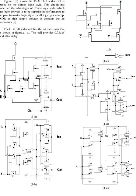
Figure 1(n) shows the TSAC full adder cell is based on the c2mos logic style. This circuit has inherited the advantages of c2mos logic style, which has been proved in to be superior in performance to all pass transistor logic style for all logic gates except XOR at high supply voltage. It contains the 26 transistors [8].
The GDI full adder cell has the 24 transistors that is shown in figure.(1-o). This cell provides 0.78µW and 50ns delay.
(1-a)
(1-b)
(1-c)
(1-d)
(1-f)
(1-g)
(1-h)
(1-i)
1-k)
(1-l)
(1-m)
(1-n)
(1-o)
Fig.1- Fifteen state of the art full adder cells .(a)10T, (b)14T, (c)CPL, (d)TFA, (e)TG-Cmos, (f)C2mos, (g)Hybrid, (h)Bridge, (i)FA24T, (j)N-Cell, (k)DPL, (l)Mod2f, (m)HPSC,
(n)TSAC,(o)FA-GDI.
Proposed 17 Transistor Full Adder Cell
This design is implemented by using both NMOS and PMOS as pass transistors. At sum, full swing output is achieved by connecting two series PMOS and two series NMOS transistors. For this XOR operation, 4 transistors are used and two sets of the same structure is used to implement that total 8 transistors are used to implement the sum output. The carry output is implemented by using following logic.
In most of the full adder circuits, carry takes the more delay. This delay affects the overall performance of the complex designs. So by reducing the delay of the carry might increase the overall performance of the system.
The carry is developed from the following table and equations:
A B Cin A
xorB Cout Logic equation
0 0 0 0 0
or or
0 0 1 0 0
or or
0 1 0 1 0
or or
0 1 1 1 1 AB or Cin.AxorB
1 0 0 1 0
or or
1 0 1 1 1 AB or Cin.AxorB 1 1 0 0 1 AB or Cin.AxorB 1 1 1 1 AB or Cin.AxorB
TABLE 1. LOGIC EQUATIONS OF CARRY Table 1 shows the logic that is used to implement carry output. The circuit diagram of proposed full adder cell is shown in figure 2. This design can be implemented in N-Well CMOS Technology by connecting Bulks of NMOS and PMOS to GND and VDD respectively.
XOR function is also a key variable in adder equation. If the generation of it is optimized, this could greatly enhance the performance of the full adder cell. It uses eight transistors to generate the XOR function
The goal of this paper is to design a high performance and low power full adder cell with the above said technique. The full adder cell has the 17 transistors that is shown in figure.2. In the first stage of this cell, the series combination of NMOS and PMOS network is used for generating XOR function. This stage shows full swing. The Sum generated from the first stage and the Carry output is generated from the first stage as well as the primary inputs.
The proposed full-adder cell schematic is shown in the figure 3.
Fig. 2 The proposed full adder cell with 17 transistors
Simulation Results
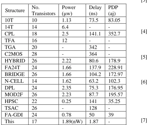
The simulation results showx the actual delay of the full adder operation. In this all the timing delays are extracted. The power consumption also from from the post lay out simulation. The comparisons shown in the table. TANNER Tool is used for design implementation and for simulation.
Structure No. Transistors Power (μw) Delay (ns) PDP (aj) 10T 10 1.13 73.5 83.05 14T 14 6.4 - - CPL 18 2.5 141.1 352.7 TFA 16 12 - - TGA 20 - 342 - C2MOS 28 - 364 - HYBRID 26 2.22 80.6 178.9 FA24T 24 1.66 137.9 228.91 BRIDGE 26 1.66 104.2 172.97 N-CELL 14 1.62 63.2 102.3 DPL 24 2.35 75.3 176.95 MOD2F 26 2.23 87.7 195.57 HPSC 22 0.25 141 35.25 TSAC 26 - 128 - FA-GDI 24 0.78 50 39 This
work
17 1.89(nW) 1.87 -
Table II. Comparison of similar works
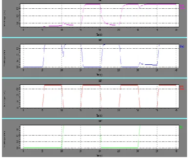
After the simulation, the layout of circuit is drawn. By the post simulation result along with a few corrections have achieved in sizes that the circuit has an accurate operation. Simulation results are performed by TSPISE based on 0.18μm CMOS technology. The power supply is 1.8v. In the table II, comparison of similar works and their results have been there. The snapshot of the waveforms at 1.8v is shown in figure 3.
Conclusion
The aim of this work is to achieve power reduction and speed increase in the full adder. In this operation new logic circuit is introduced based on equations. By using this technique such as size optimizing in full adder could reduce the power consumption. As a result, the full adder works at the 550 MHz speed with 1.89 nw power consumption. These results were obtained with spice simulation from the extracted net list of the layouts for normal parameters, room temperature and power supply at 1.8v.
REFERENCES
[1] A.Bazzazi and B. Eskafi, “Design and
Implementation of Full Adder Cell with the GDI Technique Based on 0.18μm CMOS Technology” Proceedings of the International Multiconference of engineers and Computer Scientists 2010 Vol II,IMECS 2010, March 17 -19, 2010, Hong Kong.
[2] Rabaey J.M., A. Chandrakasan, B.Nikolic, “Digital Integrated Circuits, A Design” 2nd 2002, prentice Hall, Englewood Cliffs,NJ.
[3] A. M. Shams, T. K. Darwish and M. A. Bayoumi. “Permormance
Analysis of Low Power 1-Bit CMOS full adder cells”, IEEE Transaction on VLSI Systems, Vol. 10, Feb. 2002.
[4] K.Navi, M.R.Saatchi, O.Daei, “A high speed hybrid full Adder”, European journal of scientific research.vol.26,
No.1, 2009.
[5] M.Moaiyeri, R. Faghih Mirzaee, K.Navi, “Two New Low Power and High Performance Full Adders”, Journal of Computers, Vol. 4, No.2, February 2009.
[6] C. H. Chang, J. Gu and M. Zhang, “A review of 0.18um full adder performance for tree structured arithmetic circuits”, IEEE Transactions on Very Large Scale Integration (VLSI) Systems, vol. 13, No. 6,pp.686- 695, June 2005
[7] K. Navi, O. Kavehei, M. Ruholamini, A. Sahafi, Sh. Mehrabi and N. Dadkhahi , “Low power and High Performance 1-Bit CMOS Full Adder Cell”, Journal of Computers, Vol. 3, No. 2, February 2008.
[8] Young. Woon Kim, Hae. Jun Seo, Tae.Won Cho, “A Design of High Speed 1-Bit Full Adder Cell using 0.18 μm Cmos Process”,
Proceeding of The 23rd International Technical Conference on Circuits/Systems, Computers and communications, ITC-CSCC
2008.
[9] A.R, Saberkari, SH. Shokouhi, “A Novel Low-Power-Voltage CMOS 1-Bit Full Adder Cell with the GDI Technique”, Proceeding of The 2006 IJME-INTERTECH conference .
[10] A.Bazzazi and B. Eskafi, “Design and
Implementation of Full Adder Cell with the GDI Technique Based on 0.18μm CMOS