tablets and laptops is growing. In this paper, two proposed full adder structures are implemented using XOR-XNOR gates. The optimizations of these circuits are going to be in terms of power consumption and delay because the output capacitance of adder is low. The proposed full adder structures consume 0.32µW and 0.34µW of power respectively which is small when compared to other conventional full adder structures. These full adders not only achieves low power and high speed but also give full swing with less number of transistors. To investigate the performance of the circuits Tanner Tools and HSPICE are used. This simulation is based on 90nm technology.
Index Terms: Capacitance adder, Delay, Low power, Full-Adder.
I. INTRODUCTION
Today electronic systems play a vital role as a part of our day to day life. The increased use of engineered mobile devices, such as cell phones, personal digital assistants (PDAs), requires very large scale designs with VLSI and improved power delays. The efficiency depends on the performance of dividers, comparators, multipliers, and adders which comes under arithmetic circuits which in turn show impact on numerous digital applications. A full adder acts as a core component of a complex circuit for multiplication and division, thereby affecting the overall performance of the overall system. Full adder is a basic component used in architectures of VLSI. Adder circuits are used in arithmetic logic circuit designs, processor chip like Snapdragon, Exynos, or Intel Pentium for CPU part.
In VLSI, the trade-off factors are low power consumption, delay, speed, and cost. Several logic styles full adders [1]. Every circuit has its own advantages and disadvantages based on power and delay.
The paper is organized as shown below. In Section II, the details about the circuits design for XOR-XNOR gates is discussed, in Section III proposed circuits of logic gate circuits XOR-XNOR and another new 6 full adder circuits are designed,
Revised Manuscript Received on June 05, 2019
Pyla Rajesh, ECE, Raghu Engineering College, Visakhapatnam, India. L V Santosh Kumar Y, ECE, Raghu Engineering College, Visakhapatnam, India.
H K Raghu Vamsi, ECE, Raghu Engineering College, Visakhapatnam, India.
II. REVIEWOFXORANDXNORGATES Figure 1 shows By using Double pass transistor logic (PTL) (DPL) style [1] the Full Swing XOR/XNOR circuit designed. This structure has 8 transistors. The main disadvantage of this circuit is the use of two NOT gates. This is because the NOT gate needs to drive the output capacitance. Thus, increasing the size of the transistor in the NOT gate will result in lower capacitance with larger capacitance, creating an intermediate node. Therefore, power dissipation and short circuit power are increased, delay will also increase.
Figure 2 shows the Full Swing XOR-XNOR circuit designed by using PTL [1] style. This structure has 6 transistors. This circuit has less power consumption and low delay which are much better compared to Figure 1. Here XOR circuit has lower delay than its XNOR circuit. The only problem with this circuit is the use of NOT gates in the critical path. The critical path of the XNOR circuit consists of a NOT gate that includes an NMOS transistor, so the delay of the XNOR circuit is small. However, the critical path of the XNOR circuit is composed of the NOT gate and the PMOS transistor that is slower than the NMOS. Therefore, to improve the speed of the XNOR circuit, it is necessary to increase the size of the PMOS transistor and the NOT gate.
Figure 3 shows the XOR-XNOR circuit designed using complementary pass – transistor (CPL) style [1][6]. The problem in this circuit is XOR/XNOR circuit should have feedback on outputs because of which delay increased [3] and short circuited power of the design structure. Size of transistors needed to be increased in order to overcome the circuit delay. Another drawback is having 2 NOT gates in critical path. If we remove two transistors (a NOT gate) then it will reduce the circuit’s power dissipation.
Fig. 1: Full Swing XOR/XNOR gate using double pass
Fig. 2: Full Swing XOR/XNOR gate using PTL
.
Fig. 3: Full Swing XOR/XNOR gate using CPL
Fig. 4: Full Swing XOR gate
Fig. 5: Full Swing XNOR gate
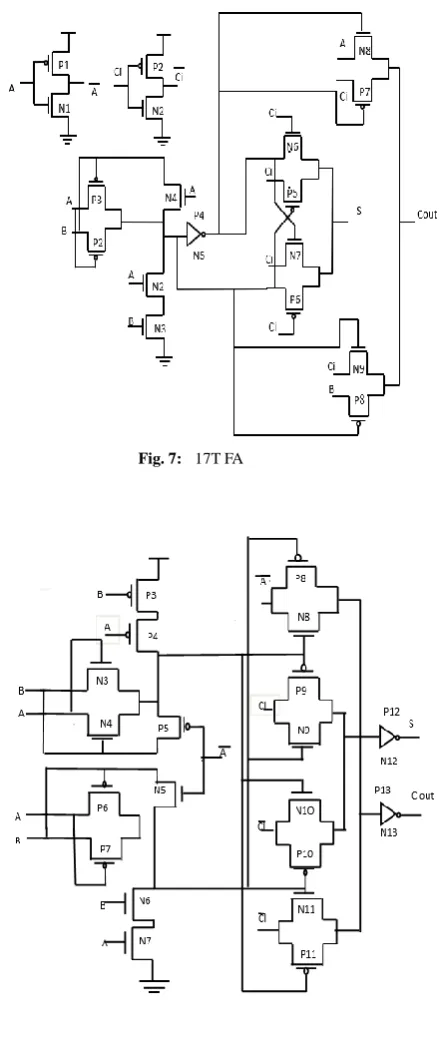
III. DIFFERENTIALFULLADDERSTRUCTURES Figure 6 show the first Full Adder circuit (20T – Full Adder) which is made up of 2 to 1 Mux gates and XOR and XNOR gate. This circuit has high power consumption NOT gate on the critical path and consists of 20 transistors. The advantages are full swing output, low power consumption, high speed and robustness to supply voltage scaling, transistor sizing [7]. The disadvantage is that when used in a chain structure such as a ripple adder, the output drive capability is reduced. Figure 7 shows the second Full Adder circuit (17T - Full Adder). This 17T – FA is designed by using the XOR gate. This is made up of 17 transistors that have less than the Figure 4 circuit. The delay of the 17T-Full Adder is greater than 20T-FA, because the NOT gate is added to the critical path of the 17T-Full Adder. The power consumption of the 17T-Full Adder [1] is less than that of the 20 T-Full Adder due to the reduced number of transistors. However, the NOT gate in this circuit increases short circuit power. Therefore, power consumption does not decrease. NOT gates improve the output capability circuit.
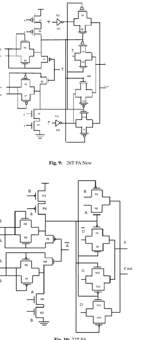
Figure 8 shows the third Full Adder circuit (26T – Full Adder Buffer). This circuit has 26 number Transistors. On critical path, there is XOR/XNOR gate, one 2-1 Multiplexer gate and NOT gate [8]. It has buffers on sum and Cout outputs. A VLSI circuit uses buffers at
[image:2.595.96.245.279.446.2] [image:2.595.63.275.482.693.2]Multiplexer gate between the buffer circuit and an output node[1].
[image:3.595.331.551.66.587.2]Figure 10 represents the fifth Full Adder circuit (22T – Full Adder). Because there is a Cbar signal that generates the sum, XOR and XNOR signals through the multipliers, they are connected to the data select lines of 2 to 1 MUX. Therefore, the capacities of XOR mode and XNOR mode become smaller, and delay [3] [5] is improved. The lower capacity of the XOR and XNOR modes results in less power and delay of 22T-full addition compared to a 20T-full addition buffer, despite the addition of two transistors. By adding the drive capability of the Cbar signal, it is superior to the previous circuit [1].
Figure 11 represents the sixth Full Adder circuit (19T – Full Adder). Due to the presence of Cbar signal which produces sum, The XOR and XNOR signals through multipliers, but are connected to the data selection lines of 2 to 1 MUXs. This reduces the capacitance in XOR and XNOR modes and improves the delay. Power consumption and 19T delay-Full Adder (FA) is lower than 17T – Full Adder (FA), but the capacity of XOR mode and XNOR mode is smaller, so adding Cbar signal drive capability will increase it You From the previous circuit [1]
Fig. 6: 20T FA
Fig. 7: 17T FA
[image:3.595.46.287.493.718.2]Fig. 9: 26T FA New
[image:4.595.311.520.66.332.2]Fig. 10:22T FA
Fig. 11:19T FA
IV. PROPOSEDFULLADDERCIRCUITS Use Figure 12 represents the first proposed Full adder. The circuit consists of 18 transistors which have two transistors less when compared to 20T – FA. This circuit consumes less power and low delay. This circuit works in non – full swing, due to this the outputs have non – full swing effect. But there is no Disadvantage in having non – full swing outputs. The proposed FA has consumed low power when compared to previous circuit 20T– FA due to the presence of less number of transistors and occupies less space due to the removal of two transistors [1][2].
Fig. 12:Proposed FA
Figure 13 represents the second proposed Full adder. The circuit consists of 15 transistors which have two transistors less when compared to 17T– FA. This circuit has power consumption and delay in very low amount. This circuit works in non – full swing, due to this the outputs have non – full swing effect. But there is no Disadvantage in having non – full swing outputs. The proposed full adder has low power
consumption when
[image:4.595.361.506.484.625.2]Fig. 13:Proposed FA 2
[image:5.595.53.265.59.272.2]A. Simulated Results and Performance Comparison Table 1: FA Comparison table
DESIGN POWER DELAY
(SUM)
DELAY (CARRY)
20T – Full Adder 19.97µW 6ns 10ns
17T Full Adder 21.410µW 2ns 6ns
26T – Full Adder Buffer
1.8072µW 2ns 8ns
26T – Full Adder New Buffer
1.5994µW 6ns 6ns
22T – Full Adder 19.902µW 8ns 1ns
19T – Full Adder 12.580µW 8ns 8ns
Proposed Full Adder 1
0.3216µW 2ns 6ns
Proposed Full Adder 2
0.34928µW 2ns 6ns
Fig. 14:Proposed FA 1
Fig. 15:Proposed FA 2
Fig. 16:Graphical Representation of Power and Delay
V. CONCLUSION
In this paper, the low power and fast FA circuits are designed by using XOR and XNOR gates. This work presents low power consumption of a 1-bit FA design in 90nm technology. The proposed FA circuits occupy less space due to number of transistors which consumes less power and which is operated at high speed when compared to the convectional FAs. The proposed FA1 circuit has been implemented by removing the P7 and N8 transistors which in turn reduces the circuit complexity. Similarly, in the proposed full adder 2 circuit is implemented by removing the P5 and N7 transistors which in turn reduces the circuit complexity. Similarly, in proposed FA 2 circuit is implemented by removing P5 and N7 transistors. As we on scaling down the transistors lengths to nano scale technologies we can reduce the power consumption from mW to μW. The sizes of all the transistors of proposed full adders are optimized in such a way that it shows low power and high speed, which is suitable for high performance ALUs.
REFERENCES
1. HAMED NASERI AND SOMAYEHTIMARCHI,“LOW-POWER AND FAST
FULL ADDER BY EXPLORING NEW XOR AND XNORGATES”.
[image:5.595.41.267.335.685.2]3. S.GOEL,A.KUMAR, AND M.BAYOUMI,“DESIGN OF ROBUST,ENERGY
-EFFICIENCY FULL ADDER FOR DEEP SUBMICRO DESIGN USING HYBRID
CMOS LOGIC STYLE,” IEEETRANS.VERY LARGE SCALE INTEGR
(VLSI)SYST, VOL.14, NO.12, PP.1309-1321,DEC.2006.
4. H.E.WESTE AND D.M.HARRIS,CMOSVLSIDESIGN:A CIRCUITS
AND SYSTEMS PERSPECTIVE, 4TH
ED, BOSTON, MA,USA:
ADDISON-WESLEY,2010
5. A.M.SHAMS AND M.A.BAYOUMI,“A NOVEL HIGH-PERFORMANCE
CMOS1-BIT FULL-ADDER CELL,”IEEETRANS.CIRCUITS SYST.II,
ANALOG DIGITAL SIGNAL PROCESS, VOL.47, NO.5, PP.478-481,MAY 2000.
6. H. T. BUI, Y. WANG, AND Y. JIANG, “DESIGN OF ROBUST,
ENERGY-EFFICIENT FULL ADDERS FOR DEEP-SUBMICROMETER DESIGN
USING HYBRID CMOS LOGIC STYLE,”IEEETRANS.CIRCUITS SYST.II,
ANALOG DIGITAL SIGNAL PROCESS, VOL. 49, NO.1, PP.25-30,JAN. 2002.
7. D.RADHAKRISHNAN,“LOW-VOLTAGE LOW-POWER CMOS FULL
ADDER,”IEEE PROC.-CIRCUITS, DEVICES SYST, VOL.148, NO.1, PP. 19-24,FEB.2001.
8. P. BHATTACHARYYA, B. KUNDU, S. GHOSH, V. KUMAR, AND A.
DANDPAT,“PERFORMANCE ANALYSIS OF A LOW-POWER HIGH-SPEED
HYBRID 1-BIT FULL ADDER CIRCUIT,” IEEE TRANS. VERY LARGE
SCALE INTEGR. (VLSI)SYST., VOL.23,NO.10, PP.2001-2008,OCT. 2015.
9. M.ALIOTO,G.DI CATALDO AND G.PALUMBO,“MIXED FULL ADDER
TOPOLOGIES FOR HIGH-PERFORMANCE LOW-POWER ARITHMETIC
CIRCUITS,”MICROELECTRON.J.,VOL.38,NO.1,PP.130-139,2007.
AUTHORSPROFILE
Pyla Rajesh was born in Visakhapatnam, India. He received his M.Tech. from JNTUK in 2013. His fields of research are VLSI SD and Low Power VLSI.
L V Santosh Kumar Y was born in Visakhapatnam, India. He received his M.Tech. from JNTUK in 2013. His fields of research are VLSI SD and Low Power VLSI.