Performance Analysis of Various Adder Circuits
on 180nm Technology
1
Preeti Verma,
2Ramnish Kumar
1,2Dept. of ECE, GJUS&T, Hisar, Haryana, India
Abstract
This paper presents a low power full adder circuit by comparing conventional 28T adder with Transmission gate adder and with the 14T adder circuitry. All full adder circuits available are designed using 0.18µm CMOS technology and all these are tested on MENTOR GRAPHICS in design architecture tool. The different circuits of full adders are simulated on the basis of speed, power consumption and area. Also, an analysis is carried out for various parameters such as delay, power dissipation etc. at different values of VDD.
Keywords
Transmission Gate (TG), Comple-mentary Metal Oxide Semiconductor (CMOS), Full Adder (FA), Very Large Scale Integration (VLSI).
I. Introduction
Power and Delay are two main parameters that need to be considered while designing any portable devices [1]. 1bit addition is the most fundamental arithmetic operation that is required in a large number of VLSI circuits. Adder is the critical component of arithmetic circuits like microprocessor, digital signal processor and arithmetic and logic unit [2]. Almost every circuit which does complex computation requires a full adder circuitry. Therefore, it is required to reduce the amount of power dissipated in the circuit and delay in adder circuit in order to maintain overall performance of the circuit [3].
This paper contains the design and performance specifications of 28T full adder cell [4] with 20T transmission gate adder using pass transistor logic and with 14T adder circuit at 180nm technology [5]. Several full Adders have been proposed on the basis of design accents such as power, delay and area [6] .The results of these Adders were obtained for different values of supply voltages.
Among these designs the circuit having less transistor count [7] using pass transistor logic has been widely used to reduce the power consumption.
This paper is organized as follows-section II presents the truth table and formula. Section III presents the CMOS conventional 28T adder for designing of full adder circuit. In section IV, the pass transistor or transmission gate logic styles to design the full adder circuit are discussed. In section V, the characteristics of 14T adder circuitry are explained. The simulation results are analyzed in section VI. At last, conclusion is presented in section VII.
II. Truth Table and Equations
The addition of input A, B and CIN will generate SUM and COUT bit. SUM and COUT is evaluated with the help of a relationship which is expressed in the form of equations.
SUM=A XOR B XOR C (1)
COUT=AB+BC+AC (2)
For odd number of inputs result of XOR and XNOR are both same. So SUM can also be expressed by another relationship which is given below.
SUM=A XNOR B XNOR C (3)
Thus with the help of above equations we evaluate the SUM and COUT.
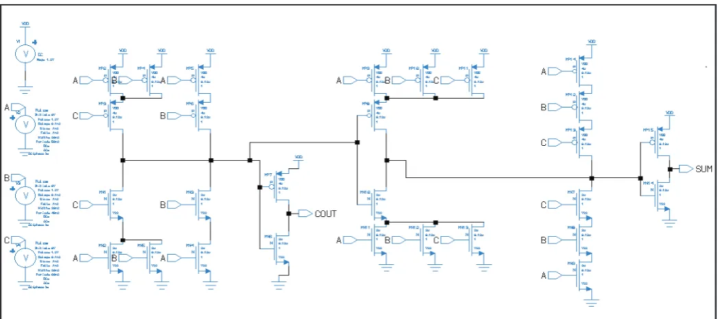
III. CMOS Based Full Adder Cell
The full adder design in regular CMOS structure consists of both PMOS and NMOS transistors [8]. These transistors are arranged in a structure formed by two complementary networks of PMOS and NMOS. In CMOS network the PMOS transistor pass 1 and NMOS transistor pass 0 .The output is having full swing and levels are not degraded. This type of circuit is called fully restored transistor logic gate pull up network and is complement of pull down network.
Advantages
The conventional full adder circuit has high noise margin and reliable operation at low voltages [9]. The layout of CMOS gate was also simplified due to complementary transistor pairs.
Disadvantages
The use of substantial number of transistors results in a very high input load, more power consumption and larger area.
Fig. 2: Waveform of 28T Adder Circuit.
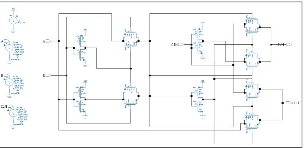
IV. 20T Transmission Gate Full Adder
Transmission adder produces buffered output of proper polarity for both sum and carry with the disadvantage of high power consumption. Pass transistor passes the signal between `drain and source instead of fixed power supply value. The main difference between CMOS logic style and the pass transistor is that the source side of logic transistor network is connected to some input signal instead of power lines.
Advantages
One pass transistor is sufficient to perform the logic operation
which results in smaller number of transistors and smaller input loads. Pass transistors require lower switching energy to charge up a node due to reduced voltage swing and also it requires less area and small amount of wiring in the network.
Disadvantages
The power dissipation in this circuit is more than conventional adder. However with same amount of power consumption this circuit will performs faster.
Fig. 4: Waveform of 20T Adder Circuit
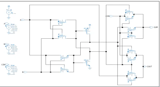
V. 14T Full Adder Circuit
This circuit contains 14 transistors to implement the full adder with the help of transmission gate along with pass transistors [10]. In this circuit the two PMOS pass transistor will perform the XOR of input bits A and B. and CIN is introduced with the help of transmission gate. In the same way carry is generated with the help of transmission gate and pass transistor logic.
Advantages
In this circuit delay is very small [11] and speed is quite high as compared to conventional adder.
Disadvantages
As delay is small in 14T adder so power dissipation is large. Because as we know power delay product remains constant.
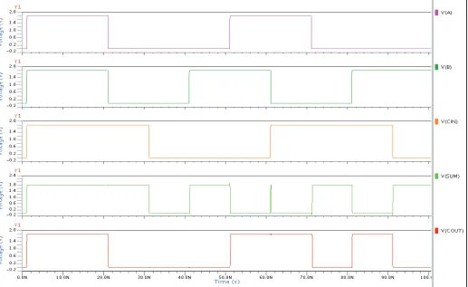
Fig. 6: Waveform of 14T Adder Circuit
VII. Observations and Analysis
In this section we will first define properties for adder schematic.
Table 1: Properties for Adder Schematic Cell Name Properties
PMOS W= 4µ, L=180n
NMOS W= 2µ, L=180n
Vpulse v = 1.8V, td= 1ns, trise = tfall= 0.1ns, T = 20ns
VDC VDC = 1.8V
Table 2: Power and Delay for 28T Adder Circuit
VDD (In
Volt) Power Dissipated (Pico Watt)
Delay (For SUM in Pico Second)
Delay (For CARRY in Pico Second)
1.8 396.57 56.155 61.768
1.6 314.63 68.242 68.567
1.4 243.89 85.635 79.631
1.2 182.06 118.72 99.719
1.0 131.70 159.43 133.23
Table 3: Power and Delay for 20T Adder Circuit
VDD (In Volt)
Power Dissipated (Pico Watt)
Delay (For SUM in Pico Second)
Delay (For CARRY in Pico Second)
1.8 696.43 6.1282 6.1276
1.6 539.79 8.3002 8.3089
1.4 408.11 4.6543 4.6462
1.2 299.14 5.4315 5.4319
1.0 210.26 9.4930 9.4986
Table:4 Power and Delay for 14T Adder Circuit
VDD (In
Volt)
Power Dissipated (Pico Watt)
Delay (For SUM in Pico Second)
Delay (For CARRY in Pico Second)
1.8 392.85 2.9716 4.6968
1.6 304.29 2.5398 4.1261
1.4 229.79 2.8134 3.8495
1.2 168.03 4.0417 5.7774
VI. Conclusion
In this paper, the main objective is to improve the performance specifications of full adder such as delay for generating sum and carry and next, to reduce the overall power dissipated in the circuit with less number of transistors in order to reduce area.
This circuit was designed with 0.18µm technology. On Mentor graphics tool and all parameters were compared with conventional adder. Due to less number of transistors and small delay 14T adder is quite useful in portable applications.
References
[1] Saradindu Panda, A.banerjee, B.maji,“Power and Delay comparison in between different types of full adder circuits”, International journal of advanced research in Electrical, Electronics and instrumentation engineering, Vol. 1, No. 3, Sept. 2012.
[2] Nidhi Tiwari, Ruchi Sharma, Rajesh Parihar, “Implementation of Area and Energy efficient Full Adder cell”, IEEE International Conference on Recent advances and Innovations in Engineering (ICRAIE-2014), May 2014.
[3] Namrata V.Bhadade, Amol k.Boke,“Design and Analyse high speed, power efficient Full adder using Digital Logic Technique”, IJAICTE, Vol. 1, Issue 7, November 2014. [4] Dan Wang, Maofeng Yang, Wu Cheng, Xuguang Guan,
Zhagming Zhu, Yintang Yang,“Novel Low Power Full Adder Cells in 180nm CMOS Technology”, IEEE (ICIEA-2009). [5] Jatinder Kumar, Praveen Kaur,“Comparative Performance
Analysis of Different CMOS Adders using 90nm and 180 nm Technology”, International Journal of Advanced Research in Computer Engineering and Technology, Vol. 2, August 2013.
[6] Mi-Chang Chang, Chih-Sheng Chang, Chih-Ping Chao, Ken-IchiMeikeiIeong, Lee-Chung Lu and Carlos H. Diaz, “Transistor and Circuit Design Optimization for Low-Power CMOS”, IEEE Transactions On Electronics Devices, Vol. 55, pp. 84-95, Jan 2008.
[7] Geetha Priya, K.Baskaran,“Low Power Full Adder with Reduced Transistor Count”, International Journal of Engineering Trends and Technology (IJETT), Vol. 4, May 2013.
[8] Nan Zhuang, Haomin Wu,“A New Design of the CMOS Full Adder”, IEEE Journal of Solid-State Circuits, Vol. 27, No.5, May 1992.
[9] Farshad Moradi, Dag. T. Wisland, Hamid Mahmoodi, Snorre Aunet, Tuan Vu Cao, Ali Peiravi,“Ultra Low Power Full Adder Topologies”, IEEE-2009.
[10] T.vigneswaran, B. Mukundhan, P. Subbarami Reddu,“A Novel Low Power, High Speed 14 Transistor CMOS Full Adder Cell with 50% Improvement in Threshold Loss Problem”, World Academy of Science, Engineering and Technology, Vol. 2, January 2008.
[11] Raju Gupta, Satya Prakash Pandey, Shyam Akashe, Abhay Vidyarthi,“Analysis and Optimization of Active Power and Delay of 10T Full Adder using Power Gating Technique at 45nm Technology”, IOSR Journal of VLSI and Signal Processing (IOSR-JVSP), Vol. 2, pp. 51-57, April 2013. [12] Hung Tien Bui, Yuke Wang, Ying Tao Jiang,“Design and
Analysis of low power 10 transistor Full Adder using Novel Xor and Xnor Gates”, IEEE Transactions on Circuits and Systems, Vol. 49, January 2012.
[13] Mi-chang chang, Chih-sheng, Chih-Ping Chao, Ken-Ichi Goto, Meikei Ieong, Lee-Chung LU, Carlos H.Diaz,“Transistor and Circuit Design Optimization for Low Power CMOS”, IEEE Transactions on Electron Devices, Vol. 55, No. 1, January 2008.
Preeti Verma received her B.tech degree in ECE from GJUS&T HISAR in 2013. She is persuing M.TECH in ECE from GJUS&T HISAR. Her area of interest is VLSI.