Article
Total bond order density as a quantum mechanical metric for materials
design: Application to chalcogenide crystals
Sahib Hasan 1, Kagendra Baral 2 Wai-Yim Ching 2,* 1 Affiliation 1; [email protected]
2 Affiliation 2; [email protected]
* Correspondence:[email protected]; Tel.:(816) 235-2503
Abstract: Materials design for processing and application requires fundamental understanding of their properties based interatomic interaction. The use of the novel concept of total bond order density (TBOD) as a single quantum mechanical metric to characterize the internal cohesion of a crystal and correlate with the calculated physical properties is particularly appealing. This requires detailed first-principles calculation of the electronic structure, interatomic bonding and related properties. In this article, we use this new concept and apply it to chalcogenide crystals based on data obtained from 25 crystals: Ag2S, Ag2Se, Ag2Te, As2S3, As2Se3, As2Te3, As4Se4, Cu2S, Cu2Se, Cu2Te,
Cu4GeS4, Cu2SnS3, Cu2SnSe3, GeS2, GeSe2, Ge4Se9, Sb2S3, Sb2Se3, Sb2Te3, SnS, SnSe, CdSe, CdTe, ZnSe,
and ZnTe. Together with the calculated optical and mechanical properties, we demonstrate the efficacy of using this novel approach for materials design that could facilitate the exploration and development of new chalcogenide crystals and glasses. Moreover, the TBOD and its partial components (PBOD) could be the key descriptors in machine learning protocol for broader scale design when a large database is available.
Key words: Chalcogenide crystals, electronic structure, optical properties, mechanical properties, total bond order density, density functional theory.
1. Introduction
The term “chalcogenide” comes from the Greek word “chalcos”. Chalcogenides are materials containing mostly one chalcogen elements (e.g. S, Se or Te) and one or more metallic ions from group IVA and VA elements. Chalcogenides are covalently bonded materials and can be amorphous or crystalline with a band gap typically ranging from 1 - 3 eV. Chalcogenide glasses or crystals are very different from the traditional glasses, silica or silicates which have much wider range of band gaps close to 8 eV[1].
Crystalline and amorphous chalcogenides are an important class of compounds very different from oxides and
nitrides but relatively less studied. This can be traced to their special interatomic bonding and more diverse
compositions. In the simplest binary composition between elements A and B, A can be from group IB in the
Periodic Table that are noble metals (Cu, Ag), or IIB (Cd, Zn), or IVA (Ge, Sn) or VA (As, Sb) while B are
chalcogene elements from group VIA (S, Se, Te).It is noted that the chalcogenide elements A and B except S
in B contain filled 3d10 or 4d10 electron shells. It is the formation of various possible chemical bonds between
A and B that makes chalcogenides a special class of materials with diverse structures and properties. The A
elements can be extended to include other metals and form ternary or quaternary mixtures and with some of
them are involved in layered 2D structures. This plethora possibility in the structure and composition of
chalcogenide makes a comprehensive study on chalcogenides an extremely challenging task. Most existing
researches in the literature concentrate on one or a few chalcogenide crystals or glasses. In this work, we study
25 crystals in which 22 are binary and 3 are ternary with A elements Cu, Ag, Cd, Zn, Ge, Sn, As, Sb and B
elements S, Se, Te. In principle, the single element chalcogene S, Se and Te should be the first step to understand
the chalcogenide compounds. However, these three elements have poor thermal stability [2-8]. This prompted
researchers to mix these three elements with other metallic elements such as As, Ag, Cu, Cd, Zn, Ge, Sb, Sn,
Cd and Zn, leading to the search for binary and multicomponent chalcogenides with special properties.
Crystalline chalcogenides are transparent in mid-infrared region. This makes them good materials for infrared
(IR) sensors and IR optics in communications, imaging, remote sensing and laser power delivery [9-12]. Within
the last two decades, research and interest in chalcogenides have grown tremendously. Many innovative devices
have been fabricated including IR optical transmitting materials, fiber optics, and integrated optical devices [13,
14]. They work efficiently at the frequency range from 1.3 to 1.55 µm and meet the high performance criteria
set by the telecom industry [15]. In medical field, the use of optical fibers to deliver high power laser light in
surgical procedures made a huge advance. However, most of these optical fibers absorb all light in the IR region
and unable to deliver a power beyond it. Thus searching for transparent materials in the IR region is crucial.
Modern applications of chalcogenides include bio-sensing, tumor detection, and IR fingerprints of lung cells
[16, 17]. S and Se can detect X-ray and they have been used for X-ray digital image detector in medical
tomography[18, 19]. They are also used to make planner and channel waveguides due to their relatively high
refractive index.
There are two other reasons that makes chalcogenides so important: Firstly, many crystalline and amorphous
chalcogenides can coexist at same composition. Secondly, they are photo-chemical sensitive with rapidly
increasing applications in technology [20]. Cu and Ag sulfides are widely used to fabricate the photon absorbers
in thin films solar cell [21, 22] and in quantum dots [23, 24]. Cu2SnS3 and Cu2SnSe3 are new promising materials
in for solar cells [25-27]. On the other hand, GeS2 and GeSe2 have several applications in cutoff devices and
photovoltaic cells [28-30]. Recently, Sb2S3, Sb2Se3, Sb2Te3, SnS, SnSe, CdSe, CdTe, ZnSe, and ZnTe are all
getting more attention due to their unique electrical, optical, switching and photovoltaic properties [31-33].
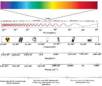
Fig.1 shows the whole electromagnetic spectrum where different optoelectronic applications are relevant. It
also shows the relevant range where the 25 crystals we studied can be useful. They are located near the infrared
region overlapping the ultraviolet region.
Over the decade, there have been extensive studies on the electronic structure and properties of chalcogenide
crystals but much less on glasses. Most of these studies focus on an isolated crystalline and glass phases or a
few chalcogenides. We briefly list some of these below focusing on Ag-and As- related systems. These are not
meant to be exhaustive and additional discussions will be added later in Section 3. Nasr et al[34] reported the
calculation of electronic structure and optical properties of crystalline Ag2S and obtained its energy gap Eg =
0.97 eV and refractive index n = 2.469. Fang et al. calculated Eg of Ag2Se and Ag2Te to be both equal to 0.00
eV[35]. For As2S3, Kaur et al.[36]reported Eg = 1.925 eV. The optical properties of amorphous As2S3 were
calculated by Synowicki et al.[37], reporting n = 2.429. Sundaram et al [38] measured the refractive index n of
glassy As30S70 to be between 2.40 - 2.42. and Fayek et al [39] reported the Eg for As2Se3 and As2Te3 glasses to
be 1.84 eV and 0.92 eV respectively. Aly revealed experimentally that n and Eg for As30Se70 to be 2.43 and 1.81
eV respectively[40]. Other experimental studies showed Eg for As20Se80 glass is 1.84 eV[41] and As2Te3 crystal
is 0.32 eV[42]. All these abundant computational and experimental data reflect the vast interest on the electronic
Fig. 1. The electromagnetic spectrum and active area of the chalcogenides.
The Cu-related chalcogenides have been investigated by several groups. Some of these crystals have very small
or zero band gap. The Eg for Cu2Te was reported by Premkumar et al [43] to be 0.0 eV andDFT calculations
by Rasander et al. [44] on Cu2Se gave Eg = 0.47 eV. Shigemi et al. showed that Cu2SnS3 and Cu2SnSe3 crystals
have Eg of 0.88 eV and 0.34 eV respectively [45]. For other chalcogenide crystals, Blaineau et al. reported Eg
for GeS2 glass to be 3.27 eV [46]. On the other hand, Fuentes-Cabrera et al.[47], calculated Eg of crystalline
GeSe2 to be 1.612 eV. Experimental studies [48-51] on Ge30Se70, Ge17Se83, Ge10Se90, and Ge14Se86 glasses
assigned their Eg and n to be (1.95, 1.78, 1.85, and 1.82 eV) and (2.26, 2.59, 2.69, and 2.60) respectively. The
Eg for Sb2S3, Sb2Se3 and Sb2Te3 crystals were reported to be 1.18 eV, 1.07 eV and 0.09 eV respectively [52],
[53]. For SnS and SnSe crystals, Guo et al. [54] reported their Eg to be 1.05 eV and 0.78 eV respectively. M.
Safari et al.[55]reported Eg for CdSe, CdTe, ZnSe, and ZnTe crystals to be 0.63 eV, 0.758 eV, 1.276 eV, and
1.27 eV respectively. We also found that computational studies of mechanical properties on chalcogenide
crystals and glasses are quite limited despite their importance in device performance. A few older publications
include amorphous GeS2 [56] and amorphous GeSe2 [57] reporting calculated values of Young’s modulus,
Shear modulus and Poisson’s ratio.
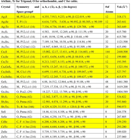
In the present work, we have studied 25 binary and ternary chalcogenide crystals between atoms of Cu, Ag, Cd,
Zn, Ge, Sn, As, and Sb and chalcogene elements (S, Se, Te). They are listed in Table 1 and their crystal
structures are sketched in Fig. S1 in the supplementary Information (SI).
In the following, we first briefly describe the methods used in the calculation. This is followed by the main
section on the results and discussion. Detailed calculations of the electronic structure, optical and mechanical
properties for these 25 chalcogenide crystals in a single paper are of considerable challenge and have not been
attempted before. Such comprehensive study enables us to make meaningful correlations among different
properties in getting a big picture especially in relation to a single quantum mechanical metric, the total bond
order density (TBOD). The paper ends with a brief conclusion and our vision for the study of chalcogenide
2. Materials and Methods
Two density functional theory (DFT) based on methods have been used in this study: Vienna Ab initio
simulation package (VASP)[58] and the orthogonal linear combination of atomic orbitals (OLCAO)
method[59]. VASP is used to optimize the crystal structures and calculate the mechanical properties. We used
the PBE-GGA potential[60] for the exchange and correlation potential with an energy cutoff of 600 eV and
sufficient number of k-points for each crystal. For small crystals such as Cu2Te, a dense k-points (3×5×3 mesh)
is used and for large crystals such as Cu2S, a smaller k-point mesh or just the Γ point in the Brillion zone are
adopted using standard Monkhorst scheme[61] The electronic and ionic force convergence criteria are set at 10
-6 eV and 10-4 eV/Å respectively.
For the electronic structure and optical properties calculations, we use the OLCAO package which was
developed in-house with the VASP-relaxed crystal structure as input. With atomic orbitals used in the basis
expansion, the OLCAO method is particularly effective to calculate the electronic structure and interatomic
bonding for both crystalline and non-crystalline materials especially those with complex structures[62, 63]. For
interatomic bonding, a more localized minimal basis (MB) used based on Mulliken scheme[64]. Eq. (1) and (2)
show the formulae for effective charge 𝑄𝛼∗ and bond order (BO) values, or the overlap population 𝜌𝛼𝛽 between
any pair of atoms (α, β).
𝑄𝛼∗ = ∑ ∑𝑖 𝑚,𝑜𝑐𝑐∑𝑗,𝛽𝐶𝑖𝛼∗𝑚𝐶𝑗𝛽𝑚𝑆𝑖𝛼,𝑗𝛽 (1)
𝜌𝛼𝛽= ∑𝑚,𝑜𝑐𝑐∑ 𝐶𝑖,𝑗 𝑖𝛼∗𝑚𝐶𝑗𝛽𝑚𝑆𝑖𝛼,𝑗𝛽 (2)
In the above equation, Siα.jβ are the overlap integrals between the ith orbital in αth atom in the jth orbital in βthatom.
Cm
jβ is the eigenvector coefficients of the mthoccupiedband. From 𝑄𝛼∗ we can obtain the so-called partial charge (PC) ∆𝑄𝛼 = 𝑄𝛼0 - 𝑄𝛼∗, or the deviation from the neutral charge 𝑄𝛼0of atom α. The BO from Eq. (2) defines
the relative strength of the bond. The summation of all BO in the crystal gives the total bond order (BO). The
total bond order density (TBOD) is obtained by normalizing the TBO with cell volume. TBOD is a single metric
to assess the internal cohesion of the crystal. It can be conveniently decomposed into partial components or the
partial bond order density (PBOD) for any structural units or groups of bonded atoms. The details for the
calculation of interatomic bonding, optical and mechanical properties are described in the supplementary
materials (SI).
3. Results and Discussion
In this section, we present the results and for the 25 chalcogenide crystals. For consistency, they are listed in
the specific order following the first character of the crystal as shown in Table 1. Table 1 lists the crystal
symmetry, space group and optimized parameters for each crystal. In all subsequent discussions, we follow
the same order for these 25 crystals in Tables and Figures. These 25 crystals start from Ag2X where X is: S,
Se, Te and end with ZnX where X is Se, Te, in this way, we can easily designate these chalcogenide crystals as
AnBm (where n = 1, 2, 4, 9 and m = 1, 2, 3, 4, 9) where A is Ag to Zn atoms,and B is S, Se, and Te atoms. In
this way, we can also easily find out the correlations between eight groups of crystals and find the changes in
their physical properties when we move from Ag to Sn atom. Any deviations in the ordering will be pointed out
as needed. We also pasted the rows in Table1 with different two colors (yellow and white) for 8 different groups
Table 1. Size and symmetry of the crystals used in our calculations and lattice parameters after full VASP relaxation, where GGA has been used as an exchange and correlation potential. (M for monoclinic, T for
triclinic, Tr for Trigonal, O for orthorhombic, and C for cubic.
Crystal Symmetry and
Space group#
a, b, c (Å), α, β, γ (in degree) #of
Atoms
Vol.(Å 3)
Ag2S M, P121/c1 (14) 4.355, 7.913, 9.233, α:90, β:122.019, γ:90 12 318.171
Ag2Se T, P1 (1) 6.616, 7.078, 5.630, α: 90.892, β: 80.305, γ: 90.109 12 263.641
Ag2Te M, P121/c1 (14) 7.336, 4.736, 10.461, α:90, β: 129.788, γ:90 12 363.449
As2S3 M, P121/c1 (14) 4.583, 10.95, 12.269, α:90, β: 111.59, γ:90 20 615.700
As2Se3 M, P121/c1 (14) 4.49, 10.94, 12.98, α:90, β: 110.68, γ:90 20 615.700
As4Se4 M, P121/c1 (14) 7.189, 14.746, 10.58, α:90, β: 114.84, γ:90 32 1121.500
As2Te3 M, C12/m1 (12) 14.947, 4.069, 10.12, α:90, β: 95.509, γ:90 20 615.490
Cu2S M, P121/c1 (14) 15.002, 12.17, 13.411, α:90, β: 116.603, γ:90 144 2448.500
Cu2Se M, P121/c1 (14) 6.453, 4.656, 6.650, α:90, β: 84.018, γ:90 12 199.800
Cu2Te M, P121/c1 (12) 8.213, 3.827, 6.153, α:90, β: 99.818, γ:90 12 193.395
Cu4GeS4 M, P121/c1 (14) 9.878, 13.247, 10.112, α:90, β: 100.572, γ:90 72 1323.194
Cu2SnS3 M, C1c1 (9) 6.699, 11.693, 6.738, α:90, β: 109.047, γ:90 24 527.797
Cu2SnSe3 M, C1c1 (9) 7.072, 12.245, 7.112, α:90, β: 109.637, γ:90 24 615.875
GeS2 M, P121/c1 (14) 6.88, 16.512, 12.864, α:90, β: 91.08, γ:90 48 1461.380
GeSe2 M, P121/c1 (14) 7.219, 17.334, 13.179, α:90, β: 91.18, γ:90 48 1619.200
Ge4Se9 O, Pca21 (29) 18.227, 7.222, 13.709, α: 90, β:90, γ:90 52 1804.589
Sb2S3 O, Pnma (62) 12.362, 3.877, 11.159, α: 90, β:90, γ:90 20 534.822
Sb2Se3 O, Pnma (62) 12.901, 4.074, 11.299, α: 90, β:90, γ:90 20 593.860
Sb2Te3 Tr, R-3m (166) 4.329, 4.329, 31.535, γ: 120.0, β: 90, α:90 15 590.973
SnS O, Pnma (62) 14.46, 4.114, 4.108, α: 90, β:90, γ:90 8 244.378
SnSe O, Pnma (62) 4.266, 4.250, 14.771, α: 90 , β:90, γ:90 8 267.805
CdSe C, F -4 3m (216) 6.208, 6.208, 6.208, α: 90 , β:90, γ:90 8 239.250
CdTe C, F -4 3m (216) 6.644, 6.644, 6.644, α: 90 , β:90, γ:90 8 293.280
ZnSe C, F -4 3m (216) 5.739, 5.739, 5.739, α: 90 , β:90, γ:90 8 189.020
ZnTe C, F -4 3m (216) 6.189, 6.189, 6.189, α: 90 , β:90, γ:90 8 237.060
3.1. Electronic structure
The electronic structure of materials is crucial for fundamental understanding on their physical and chemical
properties. The calculated results for the 25 chalcogenide crystals are shown in Figs. S2-S5 for the band
structuresand Figs. S6-S8 for the density of states (DOS). The calculated band gaps (Eg), direct (D) or indirect (ID) are listed in Table 2 together with other calculated and measured physical parameters that will be discussed
later. The electronic structure for some selected crystals are discussed in more detailed fashion in addition to
those already touched upon in the Introduction. As can be seen, GeS2 has the largest Eg of 2.484 eV among the
25 chalcogenide crystals whereas Cu2SnSe3 has the smallest Eg of 0.015 eV. Cu2Te and Ag2Te are zero-gap
As4Se4 have ID gaps while the crystals Cu4GeS4, GeX2 (X = S, Se), Sb2S3, SnX (X = S, Se), Ge4Se9, Cu2X (X
= S, Se), CdX (X = Se, Te), and ZnX (X = Se, Te) have direct gaps.
The following results on band gaps can be compared with other existing calculations as already mentioned in
the Introduction. They are widely scattered, using different methods, approaches and potentials. Some more
recent calculations are described below to compare with our calculations using OLCAO method. Since different
approaches and methods are used, considerable variations are expected. To be systematic, our discussion
follows the same sequence for the 25 crystals as listed in Table 1 and 2. Suarez et al. reported calculations of copper, silver and gold sulfide [74]. The Eg for Ag2S lies between 0.70 - 1.15 eV compared to our value of
0.823 eV. Sharma et al [75] investigated the electronic, optical and transport properties of α-and β-phases of
arsenic telluride. The Eg for ⍺-As2Te3 was for 0.480 eV, slightly less than our value of 0.627 eV. Xu et al. [76]
used hybrid functional (HSE) potentials to report Eg for monoclinic phase of Cu2S to be 1.39 eV, much larger
than our Eg of 0.299 eV. Romdhane et al. [67] used the same VASP code with GGA functional getting Eg = 0.2
eV. After GW correction, a much larger Eg of 0.9 eV is obtained. This is expected since GW correction generally
increases the band gap using DFT. Peng et al. [77] obtained Eg = 0.61 eV for crystalline Cu9S5 using a hybrid
functional HSE06. This is again consistent since LDA generally underestimate Eg. More recently, calculations
for ternary crystal Cu2SnS3 was reported by Crovetto et al. and also Chen and Persson [78, 79]. Similar trend is
observed. Using HSE06 functional, Eg was 0.83 eV and using GGA Eg was zero. Our result by using LDA has
a small Eg of 0.016 consistent with their calculations. Holomb et al. reported the Eg for amorphous GeSe2 to be
about 2.23 - 2.05 eV [80]. Our calculation for crystalline GeSe2 gives Eg = 1.80 eV, indicating the Eg for
crystalline and amorphous chalcogenides will not differ too much. We are unable find to find any calculation
on Cu4GeS4 and Ge4Se9. Apparently, our results on these two crystals are the first time results which give Eg of
0.201 eV and 1.375 eV respectively.
Table2. OLCAO results for the 25 crystals: energy gap (Eg), total bond order density (TBOD), refractive index (n), the plasma frequency (ωp), and the average effective charge on each atoms (Q*). The second column is our results, while the third column is the previous results, where (T) is for calculations and (E)
for experimental results. (D) Stands for direct band gap, while (ID) stands for indirect band gap.
Crystal Eg (eV) Eg (eV) (others) Q* (in e-) TBOD(e-/ Å 3) n, ωp (eV)
Ag2S 0.823(ID) 0.97[65] (T-D) 10.858(Ag),6.283(S) 0.01394 2.960,19.99
Ag2Se 0.298(ID) 0.00[35](T) 10.875(Ag),6.248(Se) 0.01455 4.580,18.49
Ag2Te 0.000 0.00[35](T) 11.005(Ag),5.990(Te) 0.01412 4.700,16.49
As2S3 1.906(ID) 1.925[36](T-ID) 4.506(As),6.329(S) 0.0059 2.290,18.19
As2Se3 1.523(ID) 1.84[39](E) , 1.10[66](E) 4.664(As),6.223(Se) 0.0058 3.090,18.29
As4Se4 1.494(ID) 1.20[66](E) (glass) 4.809(As),6.190(Se) 0.00717 2.770,17.69
As2Te3 0.627(ID) 0.92[39](E) 4.951(As),6.032(Te) 0.00508 6.010, 17.49
Cu2S 0.299(D) 0.20[67], 0.90[67](T-D) 10.908(Cu),6.182(S) 0.02566 3.670,20.99
Cu2Se 0.530(D) 0.47[44](T-D) 10.984(Cu),6.030(Se) 0.02225 4.120,19.99
Cu2Te 0.000 0.00[43](T) 11.158(Cu),5.683(Te) 0.02858 5.470,16.99
Cu4GeS4 0.201(D) ─ 10.930(Cu),3.384(Ge),6.223(S) 0.02234 3.430,20.19
Cu2SnS3 0.016 0.34[45](T) 11.027(Cu),3.070(Sn),6.291(S) 0.01996 3.930,19.49
GeS2 2.484(D) 3.27[46](T)(glass) 3.337(Ge),6.331(S) 0.01178 2.280,17.99
GeSe2 1.800(D) 1.612[47](T-D), 2.14[68](E) 3.534(Ge),6.232(Se) 0.00989 2.450,17.49
Ge4Se9 1.375(D) ─ 3.554(Ge),6.198(Se) 0.00932 2.480,17.99
Sb2S3 1.050(D) 1.18[52](T-D), 1.1[69](T-D) 4.242(Sb),6.505(S) 0.00604 3.780,18.29
Sb2Se3 0.550(ID) 0.99[52](T-ID), 0.75[69](T) 4.362(Sb),6.425(Se) 0.00535 4.310,17.99
Sb2Te3 0.236(ID) 0.136[70](T-ID), 0.12[71](T-D) 4.637(Sb),6.241(Te) 0.00471 7.070,17.39
SnS 0.112(D) 0.58[72](T-D) 3.481(Sn),6.518(S) 0.00534 5.010,16.29
SnSe 0.092(D) 0.22[72](T-ID) 3.525(Sn),6.474(Se) 0.00509 5.650,14.99
CdSe 1.64(D) 0.71[73](T-D) 0.584(Cd), 7.415(Se) 0.00473 2.29,17.89
CdTe 1.97(D) 0.61[73] (T-D) 0.626(Cd), 7.374(Te) 0.00399 2.35,16.1
ZnSe 1.57(D) 1.29 [73](T-D) 11.705(Zn), 6.294(Se) 0.02016 2.7,17.4
ZnTe 1.92(D) 1.23[73](T-D) 11.95(Zn), 6.05(Te) 0.01786 2.8,16.5
In other chalcogenide crystals, Ibanez et al. [69] reported the Eg of 1.1 eV and 0.75 eV for crystalline Sb2S3
and Sb2Se3 respectively. Our calculated Eg for these two crystals are 1.05 and 0.55 eV. Nasr et al. [81] obtained
Eg for Sb2S3 to be 1.88 eV, higher than ours. For crystalline Sb2Se3, Cao et al. [82] obtained Eg of 0.19 eV by
including vdW interactions, much less than our value of 0.55 eV. For crystalline Sb2Te3, the Eg obtained by
using GGA and GGA + vdW are 0.036 eV and 0.136 eV respectively [70, 83] while another study [71] gave Eg
= 0.12 eV for Sb2Te3. Kumagai et al. [84] did calculations for crystalline SnS using different
exchange-correlation functions. The Eg was 0.44 eV with LDA, 0.89 eV with GGA and 1.29 eV using HSE06. Another
study [72] reported the Eg for the SnS and SnSe to be 0.58 eV and 0.22 eV respectively. Our values for these
two crystals are 0.112 and 0.092 eV respectively. For Sb2Te3 crystal, Zhang et al.[85] reported Eg of 0.746 eV
using GGA approximation. Z. Nourbakhsh[73] calculated the Eg for the cubic crystals of CdSe, CdTe, ZnSe
and ZnTe using GGA to be 0.71, 0.61, 1.29, and 1.23 eV respectively. Our calculated Eg values for CdSe and
CdTe crystals are 1.64 and 1.97 eV respectively, much closer to experimental values of 1.75 eV [73] and 1.61
eV [86] respectively.
On the experimental side, Zhao et al. carried out IR measurements with photon energy ranging from 0.08-1.0
eV for Ag2Se crystal [87]. They concluded that it is a narrow gap semiconductor which is consistent with our
calculated gap value of 0.298 eV. In a joint experimental and computational study for glassy As2Se3 and
As4Se4 by Li et al. [66], the reported Eg for glassy As4Se4 (As2Se3) is about 1.20 eV (1.10 eV) compared to
our values of 1.494 eV and 1.523 eV for As4Se4 and As2Se3 respectively. Recently, Vaney et al [88] in a
combined computational and experiment investigation of α-As2Te3 reported its Eg to be 0.300 eV from
calculation and 0.430 eV from experiment. Our calculated value of 0.627 eV for As2Te3 is almost twice as large.
A recent by experimental study using optical transmission spectra has been conducted by Pan et al. to
investigate Eg of amorphous GeSe2 [68]. The reported value of 2.14 eV is slightly larger than our calculated
value of 1.800 eV. The experimental values of Eg for crystals Sb2S3, Sb2Se3, and Sb2Te3 by Olson et al. [89] are
1.7 eV, 1.2 eV and 0.15 - 0.2 eV respectively. These values for Sb2S3 and Sb2Se3 are larger than our calculated
values, while for the Sb2Te3, it is close to our result of 0.236 eV. Zhao [90] reported the experimental Eg for
The comparative results described above are all listed in Table 2 with the references cited. It should again be stressed that in this work, the calculation on the 25 crystals using the same method and potential can provide
meaningfully correlations of the results.
3.2 Interatomic bonding
One of the most useful results from the OLCAO calculation is the interatomic bonding between every pair of
atoms in the crystal and their bond order (BO) values which signifies the strength of the bond. By dividing the
sum of all BO values by the volume of the cell, we get the total bond order density (TBOD), a single parameter
to assess the internal cohesion and strength of the crystal [91]. The TBOD concept is particularly useful in the
present case since the data from 25 crystals over a variety of bonding configurations in different crystal types
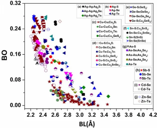
can be compared. In Fig. 2, we plotted the distribution of BO vs bond length (BL) for all atomic pairs in all 25 crystals. Obviously, this is a very busy figure that cannot reveal any pertinent details to draw useful conclusions
other than the general observation that BO usually scales with the BL. There are 36 different types of bond pairs
and the BO vs BL in each pairs can vary significantly. To dig out more details for specific trends related to each
atomic species and the crystal structure they belong, we divide them into 10 groups as shown in the insects of
Fig. 2. Please note that the groups (a), (b), (c), (d), (e) contain same atomic pairs but from different crystals.
The BO vs BL plots of these 10 groups are displayed in Figs. S9, S10 and S11 from (a) - (j) using the same scales for x- and y-axis as in Fig.2.Such detailed plots disentangle the complexity of Fig. 2 and provide new insights which are separately discussed in the first section in SI.
The TBOD is a single quantum mechanical metric obtained from the electronic structure calculations
characterizing the internal cohesion of the materials based on their interatomic interaction (BO) and the
equilibrium structure (volume). Thus the TBOD for each crystal is determined by strength of the bonds it
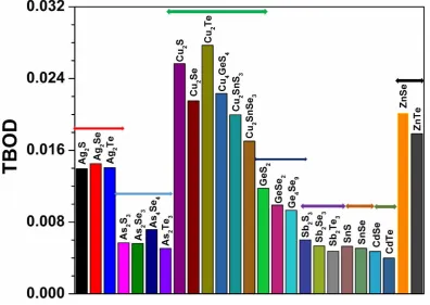
contains and the equilibrium structure of the crystal. The highest TBOD in the 25 crystals is Cu2Te followed by
Cu2S and the lowest TBOD is from CdTe closely followed by Sb2Te3 and As2Te3 (see Table 2).
In Fig. 3 we display the TBOD for the 25 crystals in the sequential order as designated earlier for Table 1. They can be roughly divided into 8 groups according to the element A in the crystal formula (Ag, As, Cu, Ge, Sb, Sn,
Cd and Zn) as indicated by the horizontal bars on top of the histogram plot. Within each group, the TBOD can
vary especially for A = Cu. Such variations are much smaller in other 7 groups. Thus we have the conclusion
the groups with A= Cu group has the highest TBOD on average followed by the A = Zn and Ag, then Ge. The
lowest average TBOD groups are A = Cd, Sn, and Sb in that order. The minor variations within each group is
controlled by the chalcogenide B element S, Se and Te. The large variations in TBOD in the A = Cu group can
be attributed to the large variations in their crystal volume. Thus we reach one important conclusion that the
strength of binary chalcogenide crystals is dictated mostly by the element A and much less by the element B.
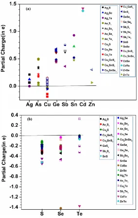
3.3 Partial charge
The partial charge (PC) distributions in chalcogenide crystals are important information related to charge
transfer and interatomic bonding. The general accepted concept is that chalcogene elements (B) receive
electrons from (A) elements or equivalently, A is electropositive and B is electronegative and they form strong
covalent bonds with ionic characters. It turns out this picture is over simplified. With 25 chalcogenide crystals
formed by 11 different elements, we are in position to analyze the PC distribution and charge transfer
mechanism in much greater detail than in the study of just one or few crystals. In Fig. 4 (a) and 4 (b), we plotted the calculated partial charge of A elements (Ag, As, Cu, Ge, Sb, Sn, Cd, Zn) and B elements (S, Se, Te)
respectively.
In general, A elements are electropositive and B elements are electronegative as expected and their values
distribute over a wide range depending on the crystals they originate from. On average, the PC value for A
elements increases from Ag to Cd, (except for the element Cu, which has much less PC), and they decrease (less negative) in B elements from S to Se to Te.The most astonishing observation to this general trend is that
Cu from Cu2Te is actually electronegative with corresponding Te in this crystal electropositive (and to a much
less extent, in Cu2Se crystal as well). This could be related to the very large size of the Te atom and they form
the Cu-Te bond with reversed mode of charge transfer. Cd element loses more charge than the all other A
elements, which is very unique property for Cd. We are not aware if this new discovery has been reported in
any previous computational or experimental studies.
3.4 Optical properties
The optical properties of these 25 chalcogenide crystals are particularly important because of their many
applications mentioned previously. They can be calculated relatively easily within the one-electron random
phase approximation using the OLCAO method. The mathematical formulae involved are explained in Section
2 in SI. The calculated real and imaginary parts of the dielectric functions for these crystals are shown in Figs. 5 (a-f), 6 (g-l), 7(m-r) and 8(s-y) refractive indices are listed in Table 2. As can be seen, each crystal has its
unique absorption features, we can only selectively discuss some of them focusing on those crystals having
Fig. 4(a): The partial charge for Ag, As, Cu, Ge, Sb, Sn, Cd, and Zn elements, (b): The partial charge of
the chalcogene elements (S, Se, Te) in the all 25 crystals. Different symbol and color indicate the crystal
is belong.
The complex dielectric functions of As2Te3 are shown in Fig. 6(g). The absorption edge of ε2(ω) occurs at 0.627 eV consistent with the direct optical gap. The maximum peak of ε2(ω) is at 2.0 eV, while the peak in real part ε1(ω) is at 0.9 eV. Since the refractive index n for the crystal is approximated as √ε1(0), the lower location of the major peak in ε1(ω) results in a relatively high refractive index for As2Te3 (n = 6.01). The calculated optical properties of Cu2Teis shown in Fig. 6(j). Results in Table 2 shows Cu2Te is a semimetal with zero gap, so ε2(ω) starts at 0.0 eV, and quickly reaches peak maximum at 0.28 eV and the n is 5.47. For the Sb2Te3 crystal, it has a small optical band gap of 0.238 eV, ε2(ω) peaks at about 1.65 eV as shown in Fig. 8(s) and it has the largest refractive index of n = 7.07 among the 25 crystals. For SnS with an indirect band gap, ε2(ω) starts at
Fig.5. Optical dielectric function for the crystals from (a) Ag2S to (f) As4Se4. The black curve for the real part (ε1), the red curve for the imaginary part (ε2).
Fig.7. Optical dielectric function for the crystals from (m) Cu2SnSe3 to (r) Sb2Se3. The black curve for the real part (ε1), the red curve for the imaginary part (ε2).
Fig.8. Optical dielectric function for the crystals from (s) Sb2Te3 to (y) ZnTe. The black curve for the real part (ε1), the red curve for the imaginary part (ε2).
From the results presented in Figs. 5-8, we see that these chalcogenide crystals in general have high refractive
indices of about 5 to 7. Because of the lack of published results on the optical properties for these crystals, we
which is close to our value of 6.01. For crystalline Cu2Te, we find an experimental study reporting n to be between 3.0 – 6.0 [92] close to what we got (n = 5.470). It should be noted that our calculated optical band gap for Cu2Te is 0.0 eV which contributed to the large n similar to other chalcogenides just discussed. The refractive index of Sb2Te3 was recently calculated by Lawal et al. [71] to be 7.482 which again is close to our result of
7.07. Rehman et al. [93] calculated the pressure dependence of the refractive index n of SnSe. The refractive index ranges 3.18 to 8.74 for pressure between 0 to 40 GPa. Our calculated value of n = 5.65 is within this range.
Finally, we present the calculated the energy loss functions (ELF) for all 25 crystals in Figs. S12, S13 and S14). ELF represents the collective excitation of excited electrons at high frequency. It main peak is defined as the
plasma frequency ωp which usually occurs at the frequency when the real part of dielectric function vanishes (ε1 (ωp) = 0). Below ωp, the incident waves will be mostly reflected. Above ωp, the material behave like a plasma, or the excited electrons are nearly free electrons. Table 2 shows the highest ωp among the 25 crystals occurs is in Cu4GeS4 (20.19 eV), while the lowest ωp is in SnSe at 14.99 eV.
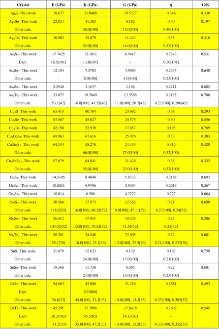
3.5 Mechanical properties
Mechanical properties for chalcogenide crystals are much less studied compared to optical properties. We
have calculated the mechanical properties of 25 chalcogenide crystals using the method described in Section 3
in SI. The calculated elastic constants are listed in Table S1 which provide a wealth of information about the stability, stiffness, brittleness, ductility, and anisotropy of these crystals [94]. The principal coefficients C11,
C22, and C33 reflects the isotropic elasticity of the crystals and they are very close. C11, C22, and C33 are related
to the unidirectional compression along the principle x-, y-, z- directions [42]. Equivalently, we say C11, C22,
and C33 reflect the resistance of the crystal to the deformation along x, y, and z directions. Table S1 shows that C33 is higher than C11 and C22 in some monoclinic crystals such as Ag2S, Ag2Se, As2S3, As2Se3, As4Se4, Cu2Se,
and Cu2SnSe3 which implies that in these crystals, they are more compressible along x- and y-axes than along
z-axis.C22 is higher than C11 and C33 in monoclinic crystals (Ag2Te, As2Te3, Cu2S, GeS2, GeSe2, Cu4SnS4) and
also in orthorhombic crystals (Ge4Se9, Sb2S3, Sb2Se3, and SnS).So these crystals are more compressible along
x- and z-axes than along y-axis. C11 is higher than both C22 and C33 in monoclinic Cu2SnS3 and Cu2Te, trigonal
Sb2Te3, orthorhombic SnSe. Accordingly, these crystals are more compressible along y- and z-axes than along
x-axis. For CdSe, CdTe, ZnSe, and ZnTe crystals, C11 = C22 = C33 since the cubic crystals are isotropic.
From elastic constants we can obtain the mechanical parameters: bulk modulus (K), shear modulus (G), Young’s modulus (E), and Poisson’s ratio (η) under VRH approximation for polycrystals as explained in Section 3 in SI [95-97]. These values are listed in Table 3. Young’s modulus measures the stiffness of the materials, bulk modulus refers to the resistance to shape deformation, and shear modulus reflects the resistance
against the shear deformation. Table 3 shows that E can vary widely among the 25 chalcogenide crystals ranging from 5.29 GPa in As4Se4 to 83.14 in ZnSe, a factor of more than 13. We are unable to find any previous
calculated or experimental elastic properties for several crystals (Ag2S, Cu2S, Cu2Se, Cu2Te, Cu4GeS4, GeS2,
GeSe2, and Ge4Se9). From the shear and bulk modulus parameters, we can express another important parameter called Pugh’s ratio, G/K [98, 99].According to Pugh’s criterion, the crystals with G/K larger than 0.571 are brittle, and those with G/K less than 0.571 are more ductile. Thus the following crystals: As2Se3, As4Se4, As2Te3,
Cu2Te, GeS2, Ge4Se9, Sb2S3, Sb2Te3, SnS, SnSe, ZnSe and ZnTe are brittle, whereas the rest of the 25 crystals
Table 3. Calculated Young modulus (E), Bulk modulus (K), Shear modulus (G), Poisson’s ratio (η), and Pugh’s
modulus ratio (G/K) for the 25 crystals. For some of these crystals, we did not find any experimental or calculated
data for the mechanical properties for comparison.
Crystal E (GPa) K (GPa) G (GPa) η G/K
Ag2S-This work 28.677 31.0408 10.5227 0.346 0.338
Ag2Se- This work
Other calc. 23.057 - 41.383 58.0[100] 8.192 12.0[100] 0.40 0.40[100] 0.197
Ag2Te- This work
Other calc. 30.983 - 35.879 52.0[100] 11.423 14.0[100] 0.35 0.37[100] 0.318
As2S3- This work
Expt. 17.7425 16.5[101] 13.1011 13.8[101] 6.9617 - 0.2743 0.30[101] 0.531
As2Se3- This work
Other calc. 12.104 - 7.5705 8.0[100] 4.9063 4.0[100] 0.2335 0.25[100] 0.648
As4Se4- This work 5.2946 3.1637 2.168 0.2211 0.685
As2Te3- This work
Other calc. 33.877 53.1[42] 19.7049 16.0[100], 41.35[42] 13.9588 11.0[100], 20.7[42] 0.2135 0.22[100], 0.286[42] 0.708
Cu2S- This work 65.413 80.704 23.692 0.36 0.293
Cu2Se- This work 53.567 45.027 20.575 0.30 0.456
Cu2Te- This work 42.156 22.939 17.657 0.193 0.769
Cu4GeS4- This work 68.963 67.616 25.926 0.33 0.383
Cu2SnS3- This work
Other calc. 64.544 - 58.278 66.0[100] 24.533 27.0[100] 0.315 0.32[100] 0.420
Cu2SnSe3- This work
Other calc. 57.879 - 64.541 55.0[100] 21.428 22.0[100] 0.35 0.32[100] 0.332
GeS2- This work 14.3145 8.4848 5.8732 0.2188 0.692
GeSe2- This work 10.0851 6.9706 3.9584 0.2613 0.567
Ge4Se9- This work 10.614 6.500 4.3222 0.227 0.664
Sb2S3- This work
Other calc. 30.566 118.2[52] 17.973 16.0[100], 80.25[52] 12.562 9.0[100], 47.11[52] 0.21 0.27[100], 0.24[52] 0.698
Sb2Se3- This work
Other calc. 26.412 104.52[52] 17.951 15.0[100], 70.52[52] 10.524 41.54[52] 0.25 0.25[52] 0.586
Sb2Te3- This work
Other calc. 58.201 55.1[76] 34.948 18.0[100], 33.1[76] 23.805 13.0[100], 22.5[76] 0.22 0.21[100],0.223[76] 0.681
SnS- This work
Other calc. 21.879 - 12.033 24.0[100] 9.139 17.0[100] 0.197 0.21[100] 0.759
SnSe- This work
Other calc. 19.566 - 11.738 24.0[100] 8.005 15.0[100] 0.22 0.25[100] 0.681
CdSe- This work
Expt. Other calc. 54.663 - 36.8[33] 43.000 53.0[86] 45.0[100], 52.2[33] 21.218 - 15.0[100], 13.3[33] 0.2881 - 0.35[100], 0.383[33] 0.493
CdTe- This work
ZnSe- This work
Expt.
Other calc.
83.1365
-
-
55.8929
62.5[102]
58.0[100], 56.5[82]
33.1990
-
28.0[100]
0.2521
-
0.3[100]
0.594
ZnTe- This work
Expt.
Other calc.
66.8251
-
-
42.3494
51.0[102]
46.0[100], 43.84[82]
27.0107
-
22.0[100]
0.2370
-
0.29[100]
0.638
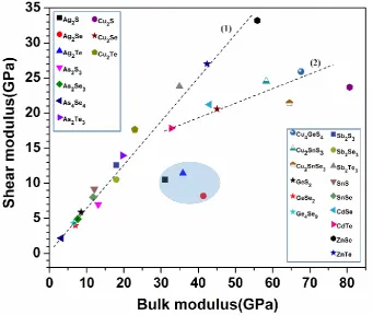
In Fig. 9, we plotted G versus K for the 25 data points with different symbols and shapes for each crystal. The
slope in this figure represents the Pugh moduli ratio G/K. As can be seen, the data can be classified into three
groups. The first group of Ag2S, Ag2Se, and Ag2Te have low G/K values of 0.388, 0.197 and 0.318
respectively are very ductile. The second group of crystals (As4Se4, As2X3 (X = Se, Te), Cu2Te, GeX2 (X = S,
Se), Ge4Se9, Sb2X3 (X = S, Se, Te), SnX (X = S, Se), and ZnX (X = Se, Te)) lie on the dashed line (1) which means that these crystals have a linear fit as shown by the dashed line number one indicating they are more
brittle (except for As2S3 and GeSe2 which are ductile crystals) . The third group consists of the 5 Cu-related
crystals: Cu2X, Cu2SnX3 (X = S, Se), and CdX (X = Se, Te), these crystals lie on the dashed line (2) referring
that these crystals are more ductile (See Table 3).
Fig.9. Bulk modulus versus shear modulus for the 25 crystals.
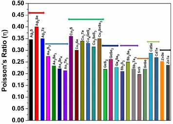
In Fig. 10, weplot the distribution of the Poisson’s ratio η of 25 crystals. Since Poisson’s ratio is closely correlated with the inverse of Pugh modulus ratio, it provides another collaborative evidence to the data
chalcogenides with noble elements Ag and Cu tends to be more brittle and those with As, Ge, Sb, Sn, Cd, Zn
are tend to be ductile.
Fig.10. distribution of the calculated Poisson’s ratio for the 25 crystals.
We now try to establish the correlation of the calculated mechanical parameters with the TBOD. In Figs. S15,
S16, and S17, we plot the Young’s modulus, bulk modulus, and shear modulus versus TBOD for the 25 crystals. It is obvious that all three moduli (E, K, G) varies with TBOD. Moreover, the correlation for the 25 crystals can
be roughly divided into 2 groups. For group 1 crystals (As2S3, As2Se3, As2Te3, Sb2S3, Sb2Se3, Sb2Te3, SnS,
SnSe, CdSe, CdTe), the E, K, G have similar values of TBOD whereas in group 2 crystals (crystals other than
group 1), they steadily increase with TBOD, while ZnSe, ZnTe crystals have the highest E among these 25
crystals. This clearly signals the new insights obtained about the mechanical properties of these 25 chalcogenide
crystals. To dig into more details on the correlations between mechanical parameters and the TBOD for the 25
crystals, we plot in Figs. S18, S19, and S20 the E, K, G for 25 crystals into 8 groups in histograms similar to Fig. 3 for TBOD. It is clear that the groups (As2X3, X = S, Se, and As4X4, X = Se) and (GeX2, X = S, Se) have the lowest Young’s modulus, while the groups (ZnX, x = Se, Te, Cu2X, X = S, Se, Te and Cu2SnX2, X = S, Se) has the highest Young’s modulus. We also notice a general feature that Cu- and Ag-related chalcogenides crystals (Ag2S, Ag2Se, Ag2Te, Cu2S, Cu2Se, Cu2Te, Cu4GeS4, Cu2SnS3, and Cu2SnSe3) show the higher
modulus values than the other crystals.
5. Conclusions
Based on the extensive DFT calculation of the electronic structure, interatomic bonding, optical and mechanical
properties of the 25 chalcogenide crystals with some of them for the first time, we are able to reveal several
new findings and hidden correlations on their properties. We succinctly summarize below the new insights
obtained and the conclusions reached in this comprehensive study using the same method and approach, and
(1) Most of these crystals are semiconductors with small band gaps and few are semimetals. The results for the
Cu4GeS4 and Ge4Se9 crystals are reported for the first time.
(2) Some of these crystals have very small energy gaps, about 0.015 – 0.299 eV. These include Cu2SnSe3,
Ag2Se, Cu2S, Cu4GeS4, Cu2SnS3, Sb2Te3, SnS, and SnSe.
(3) From the calculated bond order values, it is shown that Cu-X, Ge-X, and Sn-X (X = S, Se, Te) bonds are
much stronger than other interatomic bonds. The binary chalcogenide crystals AnBm with A = Cu, Zn and B =
S, Se, Te have the highest TBOD.
(4) We also find that the partial charge for Cu from Cu2Te is actually electronegative with corresponding Te
electropositive. This new finding has not been reported previously.
(5) The optical spectra for all 25 crystals are calculated within the random phase approximations and analyzed
in detail. They have relatively high refractive index n with some as high as from 5.01 – 7.07. This is attributed to the small band gaps with peaks in the real and imaginary dielectric functions at very low energy.
(6) The mechanical properties for these 25 crystals show the difference between those with noble metals (Ag, Zn, Cu) and those with (As, Ge, Sb, Sn, and Cd) as the “A” element in the 6 groups. The former is brittle whereas the later is more ductile. They are reasonably correlated with the TBOD thus providing us a new insight
never disclosed before.
These results and correlations can help to identify new chalcogenide crystals and glasses for potential new
applications especially in optoelectronics. They constitute a reasonable size of the database for chalcogenide
crystals. Moreover, the single quantum mechanical metric TBOD and its partial components (PBOD) could be
the key descriptors in machine learning protocol for the broader scale design when a big database is available.
Such advantage has already been demonstrated in some materials systems other than chalcogenide crystals.
Supplementary Materials: The following are available online at www.mdpi.com/xxx/s1.
Author Contributions: WC initiated the project. SH and KB did the calculation. SH and WC wrote the paper. SH made figures. All authors participated in the discussion and interpretation of the results. All authors
edited and proof-the read the final manuscript.
Funding: This research did not receive any specific grant from funding agencies in the public, commercial, or not-for-profit sectors.
Acknowledgments:
This research used the resources of the National Energy Research Scientific Computing
Center supported by DOE under Contract No. DE-AC03-76SF00098 and also the Research Computing SupportServices (RCSS) of the University of Missouri System.
Conflicts of Interest: The authors declare no competing financial interest.
References
[1] A. Zakery, S.R. Elliott, Optical nonlinearities in chalcogenide glasses and their applications, Springer, 2007. [2] R. Pan, H. Tao, H. Zang, C. Lin, T. Zhang, X. Zhao, Structure and optical properties of amorphous GeSx films
prepared by PLD, Journal of Non-Crystalline Solids, 357 (2011) 2358-2361.
[4] M. Abdullah, P. Singh, M. Hasmuddin, G. Bhagavannarayana, M. Wahab, In situ growth and ab initio optical
characterizations of amorphous Ga3Se4 thin film: A new chalcogenide compound semiconductor thin film, Scripta Materialia, 69 (2013) 381-384.
[5] A. Al-Ghamdi, S.A. Khan, S. Al-Heniti, F. Al-Agel, M. Zulfequar, Annealing and laser irradiation effects on optical constants of Ga15Se85 and Ga15Se83In2 chalcogenide thin films, Current Applied Physics, 11 (2011)
315-320.
[6] Q. Yan, H. Jain, J. Ren, D. Zhao, G. Chen, Effect of photo-oxidation on photobleaching of GeSe2 and Ge2Se3
films, The Journal of Physical Chemistry C, 115 (2011) 21390-21395.
[7] C.M. Muiva, T.S. Sathiaraj, J.M. Mwabora, Chemical bond approach to optical properties of some flash
evaporated Se 100− X Sb X chalcogenide alloys, The European Physical Journal-Applied Physics, 59 (2012). [8] G. Yang, Y. Gueguen, J.-C. Sangleboeuf, T. Rouxel, C. Boussard-Plédel, J. Troles, P. Lucas, B. Bureau, Physical
properties of the GexSe1− x glasses in the 0< x< 0.42 range in correlation with their structure, Journal of Non -Crystalline Solids, 377 (2013) 54-59.
[9] L. Liu, T. Cheng, K. Nagasaka, H. Tong, G. Qin, T. Suzuki, Y. Ohishi, Coherent mid-infrared supercontinuum
generation in all-solid chalcogenide microstructured fibers with all-normal dispersion, Optics letters, 41 (2016) 392-395.
[10] B. Zhang, W. Guo, Y. Yu, C. Zhai, S. Qi, A. Yang, L. Li, Z. Yang, R. Wang, D. Tang, Low Loss, High NA Chalcogenide Glass Fibers for Broadband Mid‐Infrared Supercontinuum Generation, Journal of the American
Ceramic Society, 98 (2015) 1389-1392.
[11] X. Dai, X. Liu, L. Liu, B. Zhu, Z. Fang, A novel image-guided FT-IR sensor using chalcogenide glass optical
fibers for the detection of combustion gases, Sensors and Actuators B: Chemical, 220 (2015) 414-419. [12] S.B. Mirov, V.V. Fedorov, D. Martyshkin, I.S. Moskalev, M. Mirov, S. Vasilyev, Progress in mid-IR lasers
based on Cr and Fe-doped II–VI chalcogenides, IEEE Journal of selected topics in quantum electronics, 21
(2015) 292-310.
[13] A. Seddon, M. Laine, Chalcogenide glasses for acousto-optic devices. II. As–Ge–Se systems, Journal of
non-crystalline solids, 213 (1997) 168-173.
[14] K. Abe, H. Takebe, K. Morinaga, Preparation and properties of Ge Ga S glasses for laser hosts,
Journal of non-crystalline solids, 212 (1997) 143-150.
[15] J.-F. Viens, C. Meneghini, A. Villeneuve, T.V. Galstian, E.J. Knystautas, M. Duguay, K. Richardson, T.
Cardinal, Fabrication and characterization of integrated optical waveguides in sulfide chalcogenide glasses, Journal of Lightwave Technology, 17 (1999) 1184.
[16] P. Sharma, N. Sharma, S. Sharda, S. Katyal, V. Sharma, Recent developments on the optical properties of thin films of chalcogenide glasses, Progress in Solid State Chemistry, 44 (2016) 131-141.
[17] N. Mehta, Applications of chalcogenide glasses in electronics and optoelectronics: A review, (2006). [18] J. Rowlands, S. Kasap, Amorphous semiconductors usher in digital x-ray imaging, Physics Today, 50 (1997)
24-30.
[19] U. Neitzel, I. Maack, S. Günther‐Kohfahl, Image quality of a digital chest radiography system based on a selenium detector, Medical physics, 21 (1994) 509-516.
[20] D. Babić, S. Rabii, J. Bernholc, Structural and electronic properties of arsenic chalcogenide molecules,
Physical Review B, 39 (1989) 10831.
[21] L. Reijnen, B. Meester, A. Goossens, J. Schoonman, Atomic layer deposition of CuxS for solar energy conversion, Chemical Vapor Deposition, 9 (2003) 15-20.
[22] H. Shen, X. Jiao, D. Oron, J. Li, H. Lin, Efficient electron injection in non-toxic silver sulfide (Ag2S) sensitized
[23] M.-C. Lin, M.-W. Lee, Cu2-xS quantum dot-sensitized solar cells, Electrochemistry Communications, 13
(2011) 1376-1378.
[24] A. Tubtimtae, K.-L. Wu, H.-Y. Tung, M.-W. Lee, G.J. Wang, Ag2S quantum dot-sensitized solar cells,
Electrochemistry Communications, 12 (2010) 1158-1160.
[25] T. Nomura, T. Maeda, T. Wada, Preparation of narrow band-gap Cu2Sn (S, Se) 3 and fabrication of film by
non-vacuum process, Japanese Journal of Applied Physics, 52 (2013) 04CR08.
[26] Y.-T. Zhai, S. Chen, J.-H. Yang, H.-J. Xiang, X.-G. Gong, A. Walsh, J. Kang, S.-H. Wei, Structural diversity and
electronic properties of Cu 2 Sn X 3 (X= S, Se): A first-principles investigation, Physical Review B, 84 (2011) 075213.
[27] Y. Ma, L. Kou, Y. Dai, T. Heine, Two-dimensional topological insulators in group-11 chalcogenide compounds: M 2 Te (M= Cu, Ag), Physical Review B, 93 (2016) 235451.
[28] L. Makinistian, E. Albanesi, First-principles calculations of the band gap and optical properties of germanium sulfide, Physical Review B, 74 (2006) 045206.
[29] T. Schwarzl, M. Böberl, W. Heiss, G. Springholz, J. Fürst, H. Pascher, Comparison of IV–VI Semiconductor
Microcavity Lasers for the Mid-Infrared with Active Regions of Different Dimensionality, in: GMe Forum 2003, 2003, pp. 103.
[30] M. Böberl, W. Heiss, T. Schwarzl, K. Wiesauer, G. Springholz, Midinfrared continuous-wave
photoluminescence of lead–salt structures up to temperatures of 190 C, Applied physics letters, 82 (2003)
4065-4067.
[31] W. Zhang, R. Yu, H.-J. Zhang, X. Dai, Z. Fang, First-principles studies of the three-dimensional strong
topological insulators Bi2Te3, Bi2Se3 and Sb2Te3, New Journal of Physics, 12 (2010) 065013.
[32] Z. Nabi, A. Kellou, S. Mecabih, A. Khalfi, N. Benosman, Opto-electronic properties of rutile SnO2 and
orthorhombic SnS and SnSe compounds, Materials Science and Engineering: B, 98 (2003) 104-115.
[33] L. Guo, S. Zhang, W. Feng, G. Hu, W. Li, A first-principles study on the structural, elastic, electronic, optical, lattice dynamical, and thermodynamic properties of zinc-blende CdX (X= S, Se, and Te), Journal of Alloys and
Compounds, 579 (2013) 583-593.
[34] T.B. Nasr, H. Maghraoui-Meherzi, H.B. Abdallah, R. Bennaceur, First principles calculations of electronic
and optical properties of Ag 2 S, Solid State Sciences, 26 (2013) 65-71.
[35] C. Fang, R. De Groot, G. Wiegers, Ab initio band structure calculations of the low-temperature phases of
Ag2Se, Ag2Te and Ag3AuSe2, Journal of Physics and Chemistry of Solids, 63 (2002) 457-464.
[36] V. Kaur, S. Tripathi, S. Prakash, The electronic structure of As2S3, in: AIP Conference Proceedings, AIP
Publishing, 2016, pp. 020433.
[37] R. Synowicki, T.E. Tiwald, Optical properties of bulk c-ZrO2, c-MgO and a-As2S3 determined by variable
angle spectroscopic ellipsometry, Thin Solid Films, 455 (2004) 248-255.
[38] S.K. Sundaram, J.S. McCloy, B.J. Riley, M.K. Murphy, H.A. Qiao, C.F. Windisch Jr, E.D. Walter, J.V. Crum, R.
Golovchak, O. Shpotyuk, Gamma radiation effects on physical, optical, and structural properties of binary As–
S glasses, Journal of the American Ceramic Society, 95 (2012) 1048-1055.
[39] S. Fayek, M. Balboul, K. Marzouk, Optical, electrical and thermal studies on (As2Se3) 3− x (As2Te3) x
glasses, Thin Solid Films, 515 (2007) 7281-7285.
[40] K.A. Aly, Optical band gap and refractive index dispersion parameters of AsxSe70Te30− x (0≤ x≤ 30 at.%)
amorphous films, Applied Physics A, 99 (2010) 913-919.
[42] H. Deng, Theoretical prediction of the structural, electronic, mechanical and thermodynamic properties
of the binary α-As2Te3 and β-As2Te3, Journal of Alloys and Compounds, 656 (2016) 695-701.
[43] T. Premkumar, J. Mani, G. Anbalagan, R. Vidya, Electronic Structure Properties of ATe and A 2 Te (A: Cu,
Ag and Cd), in: International Workshop on the Physics of Semiconductor and Devices, Springer, 2017, pp. 1151-1157.
[44] M. Råsander, L. Bergqvist, A. Delin, Density functional theory study of the electronic structure of fluorite Cu2Se, Journal of Physics: Condensed Matter, 25 (2013) 125503.
[45] A. Shigemi, T. Maeda, T. Wada, First‐principles calculation of Cu2SnS3 and related compounds, physica status solidi (b), 252 (2015) 1230-1234.
[46] S. Blaineau, P. Jund, D.A. Drabold, Physical properties of a GeS 2 glass using approximate ab initio molecular dynamics, Physical Review B, 67 (2003) 094204.
[47] M. Fuentes-Cabrera, H. Wang, O.F. Sankey, Phase stability and pressure-induced semiconductor to metal transition in crystalline GeSe2, Journal of Physics: Condensed Matter, 14 (2002) 9589.
[48] F. Abdel-Wahab, H. El Shaikh, R. Salem, Effect of Sb on the optical properties of the Ge–Se chalcogenide
thin films, Physica B: Condensed Matter, 422 (2013) 40-46.
[49] R. Kumar, D. Sharma, V. Rangra, Effect of indium incorporation on the optical properties of Ge-Se glassy
semiconductors, OPTOELECTRONICS AND ADVANCED MATERIALS-RAPID COMMUNICATIONS, 5 (2011) 1065-1068.
[50] P. Sharma, S. Katyal, Effect of substrate temperature on the optical parameters of thermally evaporated
Ge–Se–Te thin films, Thin Solid Films, 517 (2009) 3813-3816.
[51] H.M. Kotb, F.M. Abdel-Rahim, The influence of the substitution of Se for Sn on the thermal, optical and dispersion properties of Ge14Se86− xSnx thin films, Materials Science in Semiconductor Processing, 38 (2015)
209-217.
[52] H. Koc, A.M. Mamedov, E. Deligoz, H. Ozisik, First principles prediction of the elastic, electronic, and optical properties of Sb2S3 and Sb2Se3 compounds, Solid State Sciences, 14 (2012) 1211-1220.
[53] B.Y. Yavorsky, N. Hinsche, I. Mertig, P. Zahn, Electronic structure and transport anisotropy of Bi 2 Te 3 and Sb 2 Te 3, Physical Review B, 84 (2011) 165208.
[54] R. Guo, X. Wang, Y. Kuang, B. Huang, First-principles study of anisotropic thermoelectric transport properties of IV-VI semiconductor compounds SnSe and SnS, Physical Review B, 92 (2015) 115202.
[55] M. Safari, Z. Izadi, J. Jalilian, I. Ahmad, S. Jalali-Asadabadi, Metal mono-chalcogenides ZnX and CdX (X= S, Se and Te) monolayers: Chemical bond and optical interband transitions by first principles calculations, Physics
Letters A, 381 (2017) 663-670.
[56] N.D. Savchenko, T.N. Shchurova, A.B. Kondrat, V.M. Mitsa, Calculation of Elastic Constants for (GeS 2) x
(As 2 S 3) 1− x Glasses, in: AIP Conference Proceedings, AIP, 2007, pp. 1363-1366.
[57] A. Sreeram, A. Varshneya, D. Swiler, Molar volume and elastic properties of multicomponent
chalcogenide glasses, Journal of non-crystalline solids, 128 (1991) 294-309.
[58] G. Kresse, Software vasp, vienna, 1999; g. kresse, j. furthmüller, Phys. Rev. B, 54 (1996) 169.
[59] W.-Y. Ching, P. Rulis, Electronic Structure Methods for Complex Materials: The orthogonalized linear
combination of atomic orbitals, Oxford University Press, 2012.
[60] J.P. Perdew, K. Burke, M. Ernzerhof, Generalized gradient approximation made simple, Physical review
letters, 77 (1996) 3865.
[61] H.J. Monkhorst, HJ Monkhorst and JD Pack, Phys. Rev. B 13, 5188 (1976), Phys. Rev. B, 13 (1976) 5188. [62] L. Poudel, P. Rulis, L. Liang, W.-Y. Ching, Electronic structure, stacking energy, partial charge, and hydrogen
[63] K. Baral, P. Adhikari, W.Y. Ching, Ab initio Modeling of the Electronic Structures and Physical Properties
of a‐Si1− xGexO2 Glass (x= 0 to 1), Journal of the American Ceramic Society, 99 (2016) 3677-3684.
[64] R.S. Mulliken, Electronic population analysis on LCAO–MO molecular wave functions. I, The Journal of
Chemical Physics, 23 (1955) 1833-1840.
[65] T.B. Nasr, H. Maghraoui-Meherzi, H.B. Abdallah, R. Bennaceur, First principles calculations of electronic
and optical properties of Ag2S, Solid State Sciences, 26 (2013) 65-71.
[66] J. Li, D. Drabold, S. Krishnaswami, G. Chen, H. Jain, Electronic Structure of Glassy Chalcogenides As 4 Se 4
and As 2 Se 3: A Joint Theoretical and Experimental Study, Physical review letters, 88 (2002) 046803.
[67] F.B. Romdhane, O. Cretu, L. Debbichi, O. Eriksson, S. Lebègue, F. Banhart, Quasi‐2D Cu2S Crystals on
Graphene: In‐situ Growth and ab‐initio Calculations, Small, 11 (2015) 1253-1257.
[68] R. Pan, H. Tao, J. Wang, J. Wang, H. Chu, T. Zhang, D. Wang, X. Zhao, Structure and optical properties of
amorphous Ge–Se films prepared by pulsed laser deposition, Optik-International Journal for Light and Electron
Optics, 124 (2013) 4943-4946.
[69] J. Ibáñez, J. Sans, C. Popescu, J. López-Vidrier, J. Elvira-Betanzos, V.P. Cuenca-Gotor, O. Gomis, F. Manjón,
P. Rodríguez-Hernández, A. Muñoz, Structural, vibrational, and electronic study of Sb2S3 at high pressure, The
Journal of Physical Chemistry C, 120 (2016) 10547-10558.
[70] K. Zhao, Y. Wang, Y. Sui, C. Xin, X. Wang, Y. Wang, Z. Liu, B. Li, First principles study of isostructural phase
transition in Sb2Te3 under high pressure, physica status solidi (RRL)–Rapid Research Letters, 9 (2015)
379-383.
[71] A. Lawal, A. Shaari, R. Ahmed, N. Jarkoni, Sb2Te3 crystal a potential absorber material for broadband
photodetector: A first-principles study, Results in physics, 7 (2017) 2302-2310.
[72] S. Guo, L. Yuan, X. Liu, W. Zhou, X. Song, S. Zhang, First-principles study of SO2 sensors based on
phosphorene and its isoelectronic counterparts: GeS, GeSe, SnS, SnSe, Chemical Physics Letters, 686 (2017) 83-87.
[73] Z. Nourbakhsh, Structural, electronic and optical properties of ZnX and CdX compounds (X= Se, Te and S)
under hydrostatic pressure, Journal of Alloys and Compounds, 505 (2010) 698-711.
[74] J.A. Suárez, J.J. Plata, A.M. Márquez, J.F. Sanz, Structural, electronic and optical properties of copper,
silver and gold sulfide: a DFT study, Theoretical Chemistry Accounts, 135 (2016) 70.
[75] Y. Sharma, P. Srivastava, First principles investigation of electronic, optical and transport properties of α
-and β-phase of arsenic telluride, Optical Materials, 33 (2011) 899-904.
[76] Q. Xu, B. Huang, Y. Zhao, Y. Yan, R. Noufi, S.-H. Wei, Crystal and electronic structures of Cu x S solar cell
absorbers, Applied Physics Letters, 100 (2012) 061906.
[77] Z. Peng, S. Li, M. Weng, M. Zhang, C. Xin, Z. Du, J. Zheng, F. Pan, First-Principles Study of Cu9S5: A Novel
p-Type Conductive Semiconductor, The Journal of Physical Chemistry C, 121 (2017) 23317-23323.
[78] A. Crovetto, R. Chen, R.B. Ettlinger, A.C. Cazzaniga, J. Schou, C. Persson, O. Hansen, Dielectric function
and double absorption onset of monoclinic Cu2SnS3: Origin of experimental features explained by first-principles calculations, Solar Energy Materials and Solar Cells, 154 (2016) 121-129.
[79] R. Chen, C. Persson, Exploring the electronic and optical properties of Cu2Sn1− xGexS3 and Cu2Sn1−
xSixS3 (x= 0, 0.5, and 1), physica status solidi (b), 254 (2017) 1700111.
[80] R. Holomb, V. Mitsa, S. Akyuz, E. Akalin, New ring-like models and ab initio DFT study of the
medium-range structures, energy and electronic properties of GeSe2 glass, Philosophical Magazine, 93 (2013) 2549-2562.
[81] T.B. Nasr, H. Maghraoui-Meherzi, N. Kamoun-Turki, First-principles study of electronic, thermoelectric
[82] G. Cao, H. Liu, J. Liang, L. Cheng, D. Fan, Z. Zhang, The rhombohedral Sb2Se3 is also an intrinsic topological
insulator, arXiv preprint arXiv:1607.05911, (2016).
[83] H. Zhang, Y. Cheng, M. Tang, X. Chen, G. Ji, First-principles study of structural, elastic, electronic and
thermodynamic properties of topological insulator Sb2Te3 under pressure, Computational Materials Science, 96 (2015) 342-347.
[84] Y. Kumagai, L.A. Burton, A. Walsh, F. Oba, Electronic Structure and Defect Physics of Tin Sulfides: SnS, Sn 2 S 3, and Sn S 2, Physical Review Applied, 6 (2016) 014009.
[85] Y. Zhang, X. Jia, H. Sun, B. Sun, B. Liu, H. Liu, L. Kong, H. Ma, Effect of high pressure on thermoelectric performance and electronic structure of SnSe via HPHT, Journal of Alloys and Compounds, 667 (2016)
123-129.
[86] N. Data, Functional Relationships in Science and Technology, Group III, 17 (1982).
[87] Z. Zhao, S. Wang, A.R. Oganov, P. Chen, Z. Liu, W.L. Mao, Tuning the crystal structure and electronic states of Ag 2 Se: Structural transitions and metallization under pressure, Physical Review B, 89 (2014) 180102. [88] J.-B. Vaney, J.-C. Crivello, C. Morin, G. Delaizir, J. Carreaud, A. Piarristeguy, J. Monnier, E. Alleno, A. Pradel,
E.B. Lopes, Electronic structure, low-temperature transport and thermodynamic properties of polymorphic β
-As 2 Te 3, RSC Advances, 6 (2016) 52048-52057.
[89] J. Olson, H. Li, T. Ju, J. Viner, P. Taylor, Optical properties of amorphous GeTe, Sb 2 Te 3, and Ge 2 Sb 2 Te 5: the role of oxygen, Journal of applied physics, 99 (2006) 103508.
[90] L.-D. Zhao, S.-H. Lo, Y. Zhang, H. Sun, G. Tan, C. Uher, C. Wolverton, V.P. Dravid, M.G. Kanatzidis, Ultralow thermal conductivity and high thermoelectric figure of merit in SnSe crystals, Nature, 508 (2014) 373.
[91] C. Dharmawardhana, A. Misra, W.-Y. Ching, Quantum mechanical metric for internal cohesion in cement crystals, Scientific reports, 4 (2014) 7332.
[92] D. Ferizović, M. Muñoz, Optical, electrical and structural properties of Cu2Te thin films deposited by
magnetron sputtering, Thin Solid Films, 519 (2011) 6115-6119.
[93] S. ur Rehman, F.K. Butt, Z. Tariq, F. Hayat, R. Gilani, F. Aleem, Pressure induced structural and optical
properties of cubic phase SnSe: An investigation for the infrared/mid-infrared optoelectronic devices, Journal of Alloys and Compounds, 695 (2017) 194-201.
[94] S. Boucetta, Theoretical study of elastic, mechanical and thermodynamic properties of MgRh intermetallic compound, Journal of Magnesium and Alloys, 2 (2014) 59-63.
[95] W. Voigt, Lehrbuch der kristallphysik (mit ausschluss der kristalloptik), edited by bg teubner and jw edwards, leipzig berlin, Ann Arbor, Mich, (1928).
[96] A. Reuss, Berechnung der fließgrenze von mischkristallen auf grund der plastizitätsbedingung für einkristalle, ZAMM‐Journal of Applied Mathematics and Mechanics/Zeitschrift für Angewandte Mathematik
und Mechanik, 9 (1929) 49-58.
[97] R. Hill, The elastic behaviour of a crystalline aggregate, Proceedings of the Physical Society. Section A, 65
(1952) 349.
[98] S. Pugh, XCII. Relations between the elastic moduli and the plastic properties of polycrystalline pure metals, The London, Edinburgh, and Dublin Philosophical Magazine and Journal of Science, 45 (1954) 823-843.
[99] D. Varshney, S. Jain, S. Shriya, R. Khenata, High-pressure and temperature-induced structural, elastic, and thermodynamical properties of strontium chalcogenides, Journal of Theoretical and Applied Physics, 10 (2016)
163-193.
[100] M. De Jong, W. Chen, T. Angsten, A. Jain, R. Notestine, A. Gamst, M. Sluiter, C.K. Ande, S. Van Der Zwaag, J.J. Plata, Charting the complete elastic properties of inorganic crystalline compounds, Scientific data, 2 (2015)
[101] T. Rouxel, Elastic properties and short‐to medium‐range order in glasses, Journal of the American
Ceramic Society, 90 (2007) 3019-3039.
[102] H. McSkimin, D. Thomas, Elastic moduli of cadmium telluride, Journal of Applied Physics, 33 (1962)