Mesoscale Laser 3D Printing
Linas JonušauskasFemtika Ltd., Saulėtekio Ave. 15, Vilnius LT-10224, Lithuania
Laser Research Center, Vilnius University, Saulėtekio Ave. 10, Vilnius LT-10223, Lithuania
Darius Gailevičius
Laser Research Center, Vilnius University, Saulėtekio Ave. 10, Vilnius LT-10223, Lithuania
Sima Rekštytė
Laser Research Center, Vilnius University, Saulėtekio Ave. 10, Vilnius LT-10223, Lithuania
Tommaso Baldacchini
Technology and Applications Center, Newport Corporation, 1791 Deere Avenue, Irvine, California 92606, USA
Saulius Juodkazis*
Center for Micro-Photonics, Faculty of Engineering and Industrial Sciences, Swinburne University of Technology, Hawthorn, Victoria, Australia
Melbourne Center for Nanofabrication, Australian National Fabrication Facility, Clayton, Victoria, Australia
Mangirdas Malinauskas*
Laser Research Center, Vilnius University, Saulėtekio Ave. 10, Vilnius LT-10223, Lithuania
Corresponding Authors:
Keywords: direct laser writing, multiphoton processing, laser 3D nanolithography, optical 3D printing, microstructures, nanotechnology, mesoscale, two-photon polymerization, microoptics, SZ2080.
Abstract
3D meso-scale structures that can reach up to centimeters in overall size but retain micro- or nano-features, proved to be promising in various science fields ranging from micro-mechanical metamaterials to photonics and bio-medical scaffolds. In this work we present synchronization of the linear and galvano scanners for efficient femtosecond 3D optical printing of objects at the meso-scale (from sub-m to sub-cm spanning five orders of magnitude). In such configuration the linear stages provide stitch-free structuring at nearly limitless (up to tens-of-cm) working area, while galvo-scanners allow to achieve translation velocities in the range of mm/s-cm/s without sacrificing nano-scale positioning accuracy and preserving undistorted shape of the final print. The principle behind this approach is demonstrated, proving its inherent advantages in comparison to separate use of only linear stages or scanners. The printing rate is calculated in terms voxels/s, showcasing the capability to maintain an optimal feature size while increasing throughput. Full capabilities of this approach are demonstrated by fabricating structures that reach millimeters in size but still retain µm-scale features: scaffolds for cell growth, microlenses and photonic crystals. All this is combined into a benchmark structure: a meso-butterfly. Provided results show that synchronization of two scan modes is crucial for the end goal of industrial-scale implementation of this technology and makes the laser printing well aligned with similar approaches in nanofabrication by electron and ion beams.
Introduction
The 4th industrial revolution is in full swing, pushing the boundaries of scientific and industrial advances to ever new heights. The key features of this development include usage of smart devices and methodologies as well as blurring lines between different science fields [1]. Indeed, these two distinct yet highly intertwined trends induce a demand of new generation of functional meso-scale devices that must have µm-nm resolution and overall size of up to centimetres, pushing existing micro- and nano-manufacturing techniques to their absolute limit. Amidst all of this, 3D printing emerged as a new and powerful manufacturing tool of choice, as it provides nearly limitless structure geometries (within boundaries of resolution) and unmatched idea-to-object realisation rate. Optical 3D printing stands out amongst all the 3D printing techniques, as by changing the light source and its parameters a huge variety of different light-matter interaction regimes can be exploited for multi-dimensional free-form structuring [2]. The femtosecond (fs) laser-based 3D laser lithography (3DLL) is the most precise and versatile of those [3, 4] and was used to great effect in fields ranging from micromechanics [5, 6] and biomedicine [7, 8], to integrated microoptics [9, 10] and photonics [11, 12]. Additionally, tinkering with focusing properties [13], applying various interferometry techniques [14] or spatial light modulators [15] allows to tune the resolution and/or structuring rate. Combined with a huge variety of applicable materials [16, 17] it makes 3DLL an extremely attractive method for advanced functional structure fabrication.
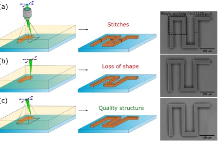
or translating the sample in relation to a stationary laser spot [Fig. 1 (b)]. In the first case, because of low inertia of galvo-scanners, high scanning velocities (up to cm/s) can be achieved. However, this approach is beneficial only while structure size does not exceed the working area of the objective, which in most cases is no more than few hundred µm. If a larger structure is needed it must be separated into segments, which are then fabricated consecutively. This introduces interfaces between them, the stitches, which reduces the overall integrity of the structure [20, 21, 23]. This can be avoided by using linear stages, yet in that case the translation velocity can potentially introduce the defects due to the inertia. On the other hand, a multi-foci approach via interference pattern or spatial light modulator (SLM) can also be employed to speed up the fabrication process, but that would require additional components in the setup which would increase its complexity. Therefore, at the moment, there is no single solution for making 3D meso-scale structures using 3DLL efficiently and without defects or technical difficulties/complications.
Here we present an approach of synchronizing linear stages and galvo-scanners. The synchronization allows realisation of a continuous scan with working field moving dynamically during manufacturing [Fig. 1 (c)]. Fabrication of mm-scale structures without loss in structuring resolution using translation velocities reaching cm/s can be realised. Stitching is also avoided. Thus, inherent weaknesses of each method of scanning are minimized while capitalizing on their strengths. We explain this approach in detail, commenting on its inherent properties. Furthermore, we illustrate the potency of this approach by showing a dramatic increase in structuring rate reaching up to 4 orders of magnitude. Finally, example structures are demonstrated with movable parts, scaffolds for regenerative medicine, mm-sized microlenses and photonic crystals.
finished structure) if the size of a structure exceeds the working field of an objective (black square). Linear positioning leads to possible loss of shape (for instance, rounded corners instead of sharp ones) when translation velocity is high (1 mm/s and more) due to stage inertia. Synchronization of both allows to continuously move working field in relation to the sample thus avoiding stitching yet still exploiting ultra-high speed and precision of structuring by employing scanner. All the given cases are illustrated by the structures fabricated in each regime at 1 cm/s translation velocities.
Results
Principles of stage synchronization
3DLL is based on nonlinear interaction between light and pre-polymer, which is confined to the focal point of an objective lens [2]. 3D nano-structure is created by moving the focal point in relation to the sample or vice versa. The latter case is achieved by moving the whole sample with various stages. These can be based on piezo crystals or other types of linear stages. While piezo positioning is the most precise (up to tenths-of-nm), it is inherently slow and has limited working volume (movement in one direction rarely exceeds few hundreds of µm). Linear stages, in contrast, can achieve translation velocities up to cm/s while still retaining theoretical precision in sub-µm range [24]. However, in real world circumstances this is hard to achieve due to inertia accumulated during fast movement of the device. Larger mass of stage helps to damp vibrational noise which is important for sub-wavelength resolution, however, forbids fast printing.
In contrast, the focal point can be moved in relation to the sample by using scanners. This can be extremely fast (up to m/s) with minimal limitations to the structuring precision [25]. Its implementation is also relatively simple. For these reasons it is still a method of choice for the most commercial 3DLL systems. The scanner limitations become apparent when the structure size starts to approach or exceed the working field of the objective lens. In the first case, outer parts of the structured object can become distorted due to various focusing aberrations [26]. Since standard optical objectives are designed for the on-axis imaging at visible spectral range, aberrations can become severe at long near IR wavelengths and larger angles of incidence. If the size of the object is further increased and exceed standard working area of high (1.4) NA objectives (up to 150 µm) stitching has to be introduced, further compromising the mechanical and optical qualities of the structure [20, 21, 23]. The working field can be increased few-fold by reducing NA, however, at the cost of printing resolution, as the voxels become larger and more elliptical [2].
corresponds to signal approximately sent every 20 µs and at scanning speed of 10 mm/s it is a trajectory of individual 0.2 µm length lines. This is sufficient, yet increasing the scanning speed up to cm/s would still be suitable for linear structures like woodpiles while limit the resolution for curved geometries like spirals of small radii. Additionally, the controller has a memory of 100 MB, which is adequate for the employed case, but also would be limiting for realization of highly curved structures at high speed unless sacrificing the resolution.
Structuring rates
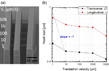
The race to achieve industrial-level manufacturing throughputs pitted different kinds of optical 3D printing methods against each other. While 3DLL is the most accurate one, users of different kinds of optical 3D printing are claiming to be capable of exceeding 3DLL by the volume that can be structured in the same amount of time [27]. However, they have to sacrifice resolution. Just listing translation velocity as the main throughput defining parameter is also insufficient, as it does not specify the size of formed features. Therefore, a lot more sensible way to talk about throughput is by defining the volume of a voxel and structuring rate in terms of voxels per second [22]. In order to calculate these values we first produced a resolution bridge, where single lines were structured with translation velocities vt of 1, 10, 100, 1000 and 10000 µm/s, speeds that are all now sustainable and usable in
repeatable fashion in 3DLL structuring with scanner-stage synchronization. Laser power was kept at 10% from the top of fabrication window, i.e. at the power at which controlled polymerization starts to turn into uncontrollable carbonization of the material (“burning”) [28]. Exposure conditions during the experiment were: 515 nm wavelength, 300 fs pulse duration, 200 kHz repetition rate. The transverse voxel size is labelled as D, while the longitudinal extension is L. Results are given in Fig. 2. The tendency for voxels to decrease in size by only a factor of ~13 as the vt increases by four orders of
Fig. 2: (a) The resolution bridge fabricated using different translation velocities vt and measured line
widths (b). Sharp decrease in line dimensions is observable. However, the aspect ratio of voxels remains in the 3-4 range.
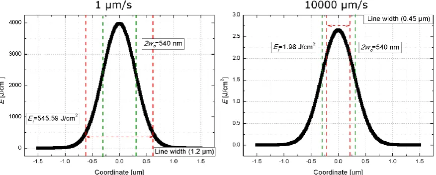
Acquired experimental results can be explained by the numerical modelling of accumulated energy dose [Fig. 3]. The results point out at dramatic difference in threshold (i.e. at line width) energy dose accumulation (Et) in both cases (545.59 J/cm2vs 1.98 J/cm2). Interestingly, at 1 µm/s the line width is
substantially larger than the spot diameter (2w0), while in the case of 10000 µm/s it is bellow
Fig. 3: Et in the centre of the line during formation at vtof 1 µm/s and 10000 µm/s and 10% below the
damage threshold of the polymer. Substantial difference in Et and resulting decrease in line width as vt
is higher.
In order to calculate the approximate volume of a voxel, we will approximate the shape of a voxel to the one of an ellipsoid in accordance with the dynamics of voxel formation. Then, the volume of a voxel Vv is [Fig. 4 (a)]:
𝑉𝑣= 4
3𝜋𝑎𝑏𝑐 = 4 3𝜋
𝐷 2
𝐷 2
𝐿 2=
1 6𝜋𝐷
2𝐿. (1)
Consequently, we can calculate that volume Vv decreases around 13.7 times when velocity vt is
increased from 1 µm/s to 10000 µm/s [Fig. 4 (b)] following dependences shown in Fig. 2b. While this is a substantial decrease, the vt increases 4 orders of magnitude, completely mitigating the possible
drop in structuring rate due to the consequentially smaller voxel volume. For instance, if we would consider a cube of 1 x 1 x 1 mm3 size, the fabrication time with 1 µm/s and 10000 µm/s would be 246903 and 174 hours respectively, which is more than 4 orders of magnitude faster in the case of highest tested translation velocity (considering a half voxel overlap). This can be explained by the increase of line volume Vl as vt is raised (following a linear slope; Fig. 4c). The line volume filling speed
is a volume of a line fabricated at a given translation velocity in one second. In that case, voxel’s D and
L are taken to calculate the area of an ellipse resembling a cross-section of a voxel and then multiplied by the distance that focal point travels at the given speed (Vl=0.25πDLvt) [Fig. 4 (a, c)]]. It allows
estimating the overall structuring rate in terms of volume per time if it is multiplied by the projected structuring time and vice versa: dividing the overall volume of object by line volume allows calculating manufacturing time of an object (making an assumption that there is no overlap and/or unnecessary movements with closed shutter). Similarly, if this quantity is divided by the volume of a single voxel the rate in voxels per second can be uncovered. This way Vl is normalized to Vv giving the rate in voxels
per second [Fig. 4 (d)]. The gain in throughput is still maintained regardless of the decreasing voxel size. Therefore, maximizing the vt is effective to enhance the overall yield of 3DLL printing.
Nevertheless, an existence of upper limit for Vv will become apparent for a high value of vt as the
SZ2080 pre-polymer), which are challenging values to achieve for most 3DLL setups even with synchronization.
While structuring rates of voxel volumes per time is a good indicator of expected throughput of 3DLL, real fabrication of complex 3D structures requires some additional considerations. Namely, one must consider voxel overlap required to produce a continuous structure as well as stage movement between different parts of the object.
Fig. 4: (a) – visualization of a single voxel, line and transverse D and longitudinal L dimensions of fabricated features. (b)-(d )are voxel volume VV, line volume Vl and voxels/second dependencies on the
translation velocity vt respectively. Slopes corresponding to a linear and diffusional spreading
(slope=0.5) of the voxel volume are shown as eye guides.
to the glass substrate, yet they can be fabricated with different parameters than the rings (namely lower overlap in vertical direction) and therefore will be excluded from the discussion.
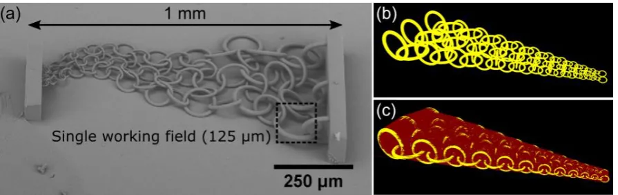
The STL file of a 3D object is hatched in XY and sliced in Z coordinates, respectively. Which can be independently set to proportional or different steps resulting to the directional fabrication accuracy/throughput. One of the advantages of the control software (3DPoli) is due to possibility of dynamical change of slicing and hatching steps of different kinds of structures on-the-fly depending on the requirements for the structure fidelity and throughput. The volume of the chain structure is 1280410 µm3. The structuring rate using v
t = 10000 µm/s is 5667 µm3/s. Therefore, theoretically, in
order to fill all the volume of the object (as shown in Fig. 5 (b)), it should take 225 seconds or around 3 and a half minutes. However, in order to achieve a continuous and relatively smooth surface the slicing and hatching steps of 0.3 µm have to be used, increasing the real structuring duration. Furthermore, there are huge gaps between different parts of the structure, that are covered by the positioning system with a closed laser shutter, creating a lot of movements that do not result in any volume polymerized. If this is done in a standard raster scanning fashion using translation stages and galvo-scanners, the time needed for fabrication is around 2 hours although synchronization is on and 1 cm/s vt is used. If optimization algorithm is applied minimizing stage movement the fabrication time
can be reduced to 26 minutes [Fig. 5 (c)]. Although this result is impressive, it is still substantially longer than the time given by theoretical calculation [Fig. 5 (c)].
Fig. 5: (a) SEM micrograph of 1 mm longgradient chain-mail (with support walls) showcasing the capability to produce relatively smooth surface with features that range from µm to hundreds of µm. A single working field of 125µm is added for the reference, showcasing that the biggest rings would not fit in it. (b) Focal point movements if only the rings would be fabricated. (c) Image showing all the movements needed to produce such structure, including ones with open shutter (yellow) and with closed shutter (red). As movements between different parts of the take up a significant portion of the laser beam repositioning between scanning, the time needed to create such structure is 26 minutes, in comparison to 3 and a half needed if only the volume will be filled.
continuous vertical rings by drawing circles in Z direction is impractical, as a shadowing effect would impinge the quality of the ring fragments, as the incident beam path would need to align with already exposed material resulting in beam distortion and overexposure [13].
Functional meso-scale structures: scaffolds for medicine
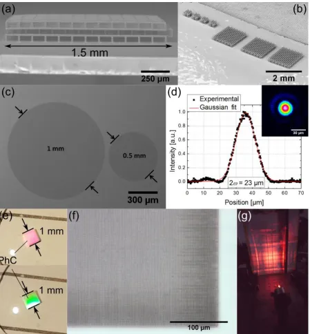
Scaffolds for cell growth are playing an increasingly prominent role in the field of regenerative medicine [7, 8]. 3DLL made objects of this kind are especially attractive as geometry of the scaffold can be custom tailored to best suit the needs of living cells [7]. Coupled with unmatched freedom in choosing the material or combining several of them in one object (so called 4D printing) promotes 3DLL as the method of choice in this field [8]. However, medicine requires large numbers of highly repeatable scaffolds, which would be at least a millimetre in size. In order to prove that synchronization of scanners and linear stages can satisfy this demand mm-sized scaffolds for cell growth were manufactured out of pure SZ2080. The overall length of the scaffold was 1.5 mm [Fig. 6 (a)]. As results are perfectly reproducible, mass production of objects of this kind is possible [Fig. 6 (b)]. Additionally, SZ2080 without photoinitiator was chosen as it should enhance biocompatibility of the material. Scaffolds of similar size and compatible fill ratio were previously produced by only using linear stages and cm/s level translation velocities, but it was done with 10x magnification 0.3 NA objective lens exploiting low resolution voxels [31]. By enabling mm-size scaffolds to be produced with high-NA objective a lot more complex and higher-resolution geometries can be achieved, enabling better mimicking of extracellular matrix which is one of the main requirements for this kind of structures. It is especially relevant as this can also be coupled with an approach of using different focusing conditions for even greater increase in fabrication throughput. Additionally, 0.8 cm/s speed results in printing time below one hour for such scaffold which is reasonable for structures needed for individual patient orientated regenerative medicine.
Functional meso-scale structures: refractive microoptics
more to the architecture of the structure, optimized exposure parameters [33] or the material development rather than the fabrication method. All these issues are resolvable by tuned and optimised engineering of exposure.
Functional meso-scale structures: photonic crystals
Fig. 6: (a) – 1.5 mm scaffold for cell growth made out of non-photosensitized SZ2080. (b) – demonstration of capabilities to produce complex bio-medicine oriented structures with on-demand scalability. (c) – SEM images of 0.5 and 1 mm lenses showing no noticeable surface or other defects, as 0.5 mm lens focuses light into a near-perfect Gaussian spot (d). (e) – photos of 1 mm sized photonic crystal before development at different angles in relation to white light illumination, which results in different colours being diffracted towards the camera. (f) – optical microscope image of the structure, revealing no defects in the lattice, which is further proved by predictable photonic crystal diffractive pattern projected onto a screen after illumination with HeNe laser beam.
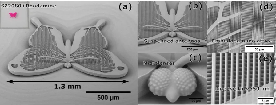
Meso-butterfly
naked eye. Rhodamine was mixed into SZ2080 to dye it bright purple colour, at the same time providing functional properties of high-yield fluorescence [35]. The 14 µm thick microcantilever-like antennas were fixed to the head. Eyes consisted of an array of few-µm-diameter functioning lenses arranged in a semi-random pattern, yet still showing high surface smoothness. As in real butterfly, wings consisted of nanolattices, which in this case were arranged in the fcc geometry to mimic photonic crystal shown previously. The line width was around 650 nm. The vt = 1 cm/s, combined with
dynamic slicing and hatching allowed to achieve printing time of 2.5 hours. Overall it shows true meso-scale capabilities of millimetre-sized structures out of functional material with true nanometre features, and optical-quality level surface roughness in critical areas, such as microlenses.
Fig. 7: A meso butterfly, created to demonstrate true meso-scale capabilities of synchronized linear stages and galvo-scanners. (a) – An overall SEM view with a naked-eye view in the inset. (b) – enlarged view of suspended antennas. (c) – eye microlens array. (d) shows embedded nanolattice with single line width of ~650 nm (e).
Discussion
From a technological point of view, this study was made possible essentially by use of electronics and software capable of synchronizing galvos with stages. Exploiting the transfer rate of 48 kHz (signal every ~20 µs) and at scanning speed of up to 10 mm/s it is realizing a trajectory of connected individual 0.2 µm length lines. This coincides well with the experimentally deduced hatching step of 0.3 µm used for fabricating gradient chain-mail and meso-butterfly (bulk part). Meanwhile the microlenses were manufactured using hatching step of 0.02 µm with translation velocity of 2 mm/s. Applying the same estimations one can see the inter-signal distance is 0.04 µm. Therefore, advances in electronic data transfer between devices is obligatory in order to further increase the speed for next generation high-resolution continuous writing setups.
Currently, the meso-scale structures are highly desired in many different fields, as they allow to introduce micro- or even nano-level interactions into a macro-sized object. So far 2D and 2.5D fabrication in this scale has been achieved by employing various lithographic technologies. However, true 3D structures are not easy to achieve. As 3DLL can be combined with other manufacturing techniques and structures can be produced on [9] or in [38] various substrates, elimination of stitching without sacrificing speed or fidelity of printing is highly promising. Additionally, if a highly tunable amplified femtosecond laser system is used capabilities of synchronization can be extended into subtractive manufacturing as well. In that case, via welding, laser assisted etching or ablation, highly complex structures can be made [39, 40]. Combining an amplified fs laser with a synchronization-capable positioning system enables a single manufacturing setup for highly complex, multi material structures.
Furthermore, the capability to perform laser fabrication with translation velocities exceeding 1 cm/s allows to have a new way of investigating the fundamentals of light-matter interaction. 3D laser polymerisation is defined by light absorption in the focal volume, hence, volumetric absorbed energy density J/cm3. The resolution of 3D fabrication is determined by the volumetric localisation of that energy, which depends on the optical or/and thermal localisation within the volume where the threshold of modification is exceeded. The modification is broadly defined by phase transitions (melting, evaporation, plasma formation), ablation, or (de)polymerisation depending of the host material.
The direct energy deposition by ultra-short laser pulses can be analysed by 3D energy deposition [41]. The spatial localization of absorbed energy in all three dimensions is estimated next. The skin depth (for the the E-field) of the optically excited material is determined by the imaginary part of the refractive index 𝑛 ≡ √𝜖 = 𝑛 + 𝑖𝜅 as 𝑙𝑎𝑏𝑠= 𝑐/(𝜔𝜅) = 𝜆/(2𝜋𝜅), it is 𝑙𝑎𝑏𝑠= 2 for the intensity 𝐼 ∝ 𝐸2. The lateral dimension of the energy deposition is defined by the focal spot which diameter can be
estimated as 2𝜔0= 1.22𝜆/𝑁𝐴 for the wavelength 𝜆 and the numerical aperture NA of the focusing
lens. The depth-of-focus usually estimated via the Rayleigh length, 𝑧𝑅, as 2𝑧𝑅 = 2𝜋𝜔02/𝜆 is much
larger than the actual depth of energy deposition (the skin depth), 𝑙𝑎𝑏𝑠. This is the key difference when
nonlinear energy deposition has to be estimated.
The absorbed energy density per volume [J/cm3] at the end of the laser pulse is 𝑊
𝑎𝑏𝑠= 2𝐴𝐹𝑝/𝑙𝑎𝑏𝑠,
where the integral fluence per pulse is, 𝐹𝑝= ∫0 𝑡𝑝
(Δ𝜀𝑑)𝑖𝑚≃ 𝜔𝑝𝑒2
𝜔2 𝜐𝑒 𝜔 = 𝑛𝑒 𝑛𝑐𝑟 𝜐𝑒
𝜔, (2)
where 𝜔𝑝𝑒= √4𝜋𝜀2/𝑚𝑒 is the cyclic electron plasma frequency, 𝑒, 𝑚𝑒 are the electron charge and
mass, respectively, 𝑛𝑒is the electron density, 𝜐𝑒is the electron relaxation frequency (electron-phonon
in solid state material), 𝑛𝑐𝑟 = 𝜔2𝑚𝑒/(4𝜋𝑒2) is the critical plasma density which was 4.21 x 1021 cm-3
at the λ = 515 nm wavelength in this study. The permittivity at the pre-breakdown in dielectric medium is 𝜀𝑑 ≃ 𝑛02+ 𝑖 × (Δ𝜀𝑑)𝑖𝑚 = 𝑛02+ 𝑖2𝑛0𝜅 , where n0 is the real part of an unperturbed refractive index
[42]. Hence, the skin depth with use of Eqn. (2) can be expressed as [42]:
𝑙𝑎𝑏𝑠= 𝜆 2𝜋𝜅=
𝑛0𝜆 𝜋(Δ𝜀𝑑)𝑖𝑚
=2𝑐𝑛0 𝜐𝑒
𝑛𝑐𝑟 𝑛𝑒
, (3)
and is defining the depth (axial) localization of the energy deposition. The absorbed energy density over the focal spot:
𝑊𝑎𝑏𝑠= 𝐴0 𝜐𝑒 𝑐𝑛0
𝑛𝑒 𝑛𝑐𝑟𝐹𝑝∝
𝑛𝑒
𝑛𝑐𝑟𝐹𝑝 (4)
where the unperturbed absorbance 𝐴0≡ 4𝑛0/[(𝑛0+ 1)2+ 𝜅2] ≃ 4𝑛0/(𝑛0+ 1)2 is neglecting the
imaginary part of the refractive index, 𝜅. Equation 4 shows that as the electron density, ne, is
approaching critical, the most efficient energy deposition occurs since the ne/ncr approaches the
maximum value of unity. This corresponds to the most efficient use of light.
For the nonlinear absorption via n-photon process, the generation of electrons 𝑛𝑒∝ 𝐼𝑝𝑛∼ 𝐹𝑝𝑛. It
begins to saturate as the critical density, ncr, is approached and the breakdown region behaves
metal-like. The absorbed energy in the skin layer is proportional to the fluence, 𝑊𝑎𝑏𝑠∼ 𝐹𝑝.
From the scaling shown above (Eqn. 4), the role of strong pulse accumulation and changes of material absorption result in a larger energy deposition. The nonlinearity of energy deposition is decreasing as
𝑛 𝑒 → 𝑛𝑐𝑟 . This leads to saturation. This behavior is expected to be generic when the observed
characteristic of light-matter interaction depends on the pre-excitation (ne in the analysis above). In the case of laser polymerisation and strong pulse-to-pulse overlap we expect this behavior. Thermal accumulation is also usually increasing the imaginary part of permittivity.
Materials and methods
3DLL was performed using nanopolymerization system in Vilnius University Laser Research Center and Laser Nanofactory setup in Femtika Ltd. [Fig. 8]. Details on the first setup can be found elsewhere [28]. The Light source in the Laser Nanofactory - laser Pharos (Light Conversion Ltd.) operating at 300 fs pulse duration, 200 kHz repetition rate and 1030 wavelength. Harmonic generator Hiro (Light Conversion Ltd.) converts fundamental wavelength to 515 nm radiation. Laser beam is then expanded via 3x telescope to completely fill the objective aperture. Positioning is realized using synchronized linear stages (ANT130XY-160 (Aerotech Inc.)) for XY plane, ANT130LZS-060, (Aerotech Inc.) for Z direction) and galvo-scanners (AGV-10HPO (Aerotech Inc.)). Real time imaging of fabrication is done by illuminating sample with LED and then imaging with a CMOS camera. The whole setup is controlled by 3DPoli software (Femtika Ltd.).
Fig. 8: Schematics of Laser Nanofactory setup used in this work. Here PPis a phase plate, P denotes thin film polarizers together with PP forming a power attenuation unit, M are the mirrors, RPM – removable power meter, T – telescope, expanding laser beam 3 times, obj – objective lens. LED illuminates the sample for real-time monitoring of fabrication process. For wavelength tuning second harmonic crystal, harmonic generator or parametric generator can be used.
Acknowledgements
The financial support from the Research Council of Lithuania funding programme “Towards Future Technologies” grant S-LAT-17-2 „Optical 3D micro-/nano-processing of bioplastics (OPTIBIOFORM)” is gratefully acknowledged.
Conflict of interests
Authors declare no conflict of interest.
Contributions
LJ performed majority of the experiments and wrote the main part of the manuscript. DG and SR fabricated photonic and scaffold structures, respectively. All authors discussed and did interpretation of the results, essentially contributed to the preparation of the final manuscript.
References
1: Lasi, H., Fettke, P., Feld, T. & Hoffmann M. Industry 4.0. BISE6(4), 239-242 (2014).
2: Jonušauskas, L., Juodkazis, S. & Malinauskas, M. Optical 3D printing: bridging the gaps in the mesoscale. J. Opt.20, 053001 (2018).
3: Zhang, Y. L., Chen, Q. D., Xia, H & Sun, H. B. Designable 3D nanofabrication by femtosecond laser direct writing. NanoToday5(5), 435-448 (2010).
4: Malinauskas, M., Žukauskas, A., Hasegawa, S., Hayasaki, Y., Mizeikis, V. et al. Ultrafast laser processing of materials: from science to industry. Light. Sci. Appl.5, e16133 (2016).
5: Schizas, C., Melissinaki, V., Gaidukevičiūtė, A., Reinhardt, C., Ohrt, C. et al. On the design and fabrication by two-photon polymerization of a readily assembled micro-valve. Int. J. Adv. Manuf. Technol. 48(5-8), 435-441 (2010).
6: Frenzel, T., Kadic, M. & Wegener, M. Three-dimensional mechanical metamaterials with a twist.
Science258(6366), 1072-1074 (2017).
7: Mačiulaitis, J., Deveikytė, M., Rekštytė, S., Bratchikov, M., Darinskas, A. et al. Preclinical study of SZ2080 material 3D microstructured scaffolds for cartilage tissue engineering made by femtosecond direct laser writing lithography. Biofabrication7, 015015 (2015).
9: Gissibl, T., Thiele, S., Herkommer, A. & Giessen, H. Two-photon direct laser writing of ultracompact multi-lens objectives. Nat. Photon.10(8), 554-560 (2016).
10: Dietrich, P.-I., Blaicher, M., Reuter, I., Billah, M., Hoose, T., et al. In situ 3D nanoprinting of free-form coupling elements for hybrid photonic integration. Nat. Photon. 12, 241-247 (2018).
11: Aristov, A.I., Manousidaki, M., Danilov, A., Terzaki, K., Fotakis, C. et al. 3D plasmonic crystal metamaterials for ultra-sensitive biosensing. Sci. Rep.6, 25380 (2016).
12: Koschny, T., Soukoulis, C. M. & Wegener, M. Metamaterials in microwaves, optics, mechanics, thermodynamics, and transport. J. Opt.9, 084005 (2017).
13: Jonušauskas, L., Rekštytė, S. & Malinauskas, M., Augmentation of direct laser writing fabrication throughput for three-dimensional structures by varying focusing conditions. Opt. Eng. 53(12), 125102 (2014).
14: Garliauskas, M., Stankevičius, E. & Račiukaitis, G. Laser intensity-based geometry control of periodic submicron polymer structures fabricated by laser interference lithography. Opt. Express 7(1), 179-184 (2017).
15: Yang, L., El-Tamer, A., Hinze, U., Li, J., Hu, Y., et al. Parallel direct laser writing of micro-optical and photonic structures using spatial light modulator. Opt. Lasers Eng.70, 26-32 (2015).
16: Farsari, M., Vamvakaki, M. & Chichkov, B.N. Multiphoton polymerization of hybrid materials. J. Opt.12, 124001 (2010).
17: Barner-Kowollik, C., Bastmeyer, M., Blasco, E., Delaittre, G., Müller, P., et al. 3D Laser Micro‐ and Nanoprinting: Challenges for Chemistry. Angew. Chem. Int. Ed.56, 15828-15845 (2017).
18: Sun Y.-L., Dong W.-F., Niu L.-G., Jiang T., Liu D.-X. et al. Protein-based soft micro-optics fabricated by femtosecond laser direct writing. Light. Sci. Appl. 3, e129 (2014).
19: Jiang, L., Xiong, W., Zhou, Y., Liu, Y., Huang X. et al. Performance comparison of acrylic and thiol-acrylic resins in two-photon polymerization. Opt. Express 24(12), 13687-13701 (2016).
20: Oakdale, J. S., Smith, R. F., Forien, J.-B., Smith, W. L., Ali, S. J. et al. Direct laser writing of low-density interdigitated foams for plasma drive shaping. Adv. Funct. Mater.27(43), 1702425 (2017).
21: Accardo, A., Blatche, M.-C., Courson, R., Loubinoux, I., Thibault, C. et al. Multiphoton direct laser writing and 3D imaging of polymeric freestanding architectures for cell colonization. Small 19(27), 1700621 (2017).
22: Vyatskikh, A., Delalande, S., Kudo, A., Zhang, X., Portela, C. M. et al. Additive manufacturing of 3D nano-architected metals. Nat. Commun.9, 593 (2018).
24: Torgersen, J., Ovsianikov, A., Mironov, V., Pucher, N., Qin, X. et al. Photo-sensitive hydrogels for three-dimensional laser microfabrication in the presence of whole organisms. J. Biomed. Opt. 17(10), 105008 (2012).
25: Alharbi, N., Osman, R. & Wismeijer, D. Effects of build direction on the mechanical properties of 3D-printed complete coverage interim dental restorations. J. Prosthet. Dent.115(6), 760-767 (2016).
26: Ai, J., Lv, M., Jiang, M., Liu, J. & Zeng, X. Focused laser lithographic system for efficient and cross-scale fabrication of large-area and 3D micro-patterns. Opt. Lasers Eng.107, 335-341 (2018).
27: Chen, X., Liu, W., Dong, B., Lee, J., Ware, H. O. T. et al. High‐speed 3D printing of millimeter‐ size customized aspheric imaging lenses with sub 7 nm surface roughness. Adv. Mater. 30(18), 1705683 (2018).
28: Jonušauskas, L., Gailevičius, D., Mikoliūnaitė, L., Sakalauskas, D., Šakirzanovas S. et al. Optically clear and resilient free-form µ-optics 3D-printed via ultrafast laser lithography. Materials 10(1), 12 (2017).
29: Waller E. H. and Freymann G., Spatio-Temporal Proximity Characteristics in 3D μ-Printing via Multi-Photon Absorption. Polymers8(8), 297 (2016).
30: Sakellari I., Kabouraki E., Gray D., Purlys V., Fotakis C. et al. Diffusion-Assisted High-Resolution Direct Femtosecond Laser Writing. ACS Nano6(3), 2302-2311 (2012).
31: Danilevičius, P., Rekštytė, S., Balčiūnas, E., Karaniauskas, A., Širmenis et al. Direct laser fabrication of polymeric implants for cardiovascular surgery. Mater. Sci.18(2), 145-149 (2012).
32: Ovsianikov, A., Viertl, J., Chichkov, B., Oubaha, M., MacCraith, B. et al. Ultra-low shrinkage hybrid photosensitive material for two-photon polymerization microfabrication. ACS Nano2(11), 2257-2262 (2008).
33: Žukauskas, A., Matulaitienė, I., Paipulas, D., Niaura, G., Malinauskas, M. et al. Tuning the refractive index in 3D direct laser writing lithography: towards GRIN microoptics. Las. Photon. Rev.9(6), 706-712 (2015).
34: Rekštytė, S., Jonavičius, T., Gailevičius, D., Malinauskas, M., Mizeikis, V. et al. Nanoscale Precision of 3D Polymerization via Polarization Control. Adv. Opt. Mater.4(8), 1209-1214 (2016).
35: Žukauskas, A., Malinauskas, M., Kontenis, L., Purlys, V., Paipulas, D. et al. Organic Dye Doped Microstructures for Optically Active Functional Devices Fabricated via Two-Photon Polymerization Technique. Lith. J. Phys. 50(1), 55-61 (2010).
36: Dehaeck, S., Scheid, B., Lambert, P. Adaptive stitching for meso-scale printing with two-photon lithography. Additive Manufacturing 21, 589-597 (2018).
38: Wu, D., Wu, S.-Z., Xu, J., Niu, L.-G., Midorikawa, K. et al. Hybrid femtosecond laser microfabrication to achieve true 3D glass/polymer composite biochips with multiscale features and high performance: the concept of ship-in-a-bottle biochip. Las. Photon. Rev.8(3), 458-467 (2014).
39: Jonušauskas, L., Rekštytė, S., Buividas, R., Butkus, S., Gadonas, R. et al. Hybrid subtractive-additive-welding microfabrication for lab-on-chip (LOC) applications via single amplified femtosecond laser source. Opt. Eng.56(9), 094108 (2017).
40: Tičkūnas, T., Perrenoud, M., Butkus, S., Gadonas, R., Rekštytė, S. et al. Combination of additive and subtractive laser 3D microprocessing in hybrid glass/polymer microsystems for chemical sensing applications. Opt. Express25(21), 26280-26288 (2017).
41: Hsu, W.-H., Masim, F., Balčytis, A., Juodkazis, S. & Hatanaka, K. Dynamic position shifts of X-ray emission from a water film induced by a pair of time-delayed femtosecond laser pulses. Opt. Express 25(20), 24109-24118 (2017).