Thesis by
Muhammad Mujeeb-U-Rahman
In Partial Fulfillment of the Requirements for the degree of
Doctor of Philosophy
CALIFORNIA INSTITUTE OF TECHNOLOGY Pasadena, California
2014
2014
Dedicated to
To my parents Muhammad Latif Babar and Musfra Begum,
my siblings,
my Wife Zain Javeria and our kids
and has enabled incredible miniaturization of the computing industry. It also provides options for designing different subsystems on the same platform in a monolithic process with very high yield. This choice then leads to actual designs of subsystems in the CMOS technology using different possible methods. Careful comparison of these subsystems provides insights into different design adjustments that are made until the desired functions are achieved at the desired size scale. Integration of all these compatible subsystems in the same platform is shown to provide the smallest possible sensing platform to date.
Contents
Chapter 1 Problem Introduction ... 26
1.1 Biomedical Measurements: State-of-the-Art ... 28
1.2 Miniaturized Implants ... 35
1.3 Need for new Technology ... 36
1.4 Thesis Focus ... 37
1.5 Thesis Outline ... 37
Chapter 2 System Design ... 39
2.1 Design Perspectives ... 40
2.1.1 Biocompatibility ... 44
2.2 Proposed Design ... 46
2.3 Summary ... 48
Chapter 3 Integrated Sensor ... 49
3.1 Basic Electrochemistry ... 51
3.2 Sensor Design and Operation ... 53
3.3 Material Aspects ... 62
3.5 Electrochemical Measurements ... 75
3.6 Surface Functionalization ... 82
3.7 Enzyme Kinetics ... 84
3.8 Glucose Sensing ... 87
3.8.1 Testing in Body Fluids ... 94
3.8.2 Interference Issues ... 97
3.8.3 Lifetime and Repeatability ... 103
3.8.4 Optimization of Sensor Response ... 107
3.9 Nucleic Acid Sensing ... 110
3.9.1 Sensor Design ... 110
3.9.2 Functionalization ... 110
3.9.3 Results ... 112
3.10 Protein Sensing ... 115
3.10.1 Sensor Design and Testing ... 115
3.11 pH Sensing ... 117
3.12 Simultaneous Sensing of Multiple Analyte ... 119
3.13 Comparison of Electrochemical Measurement Techniques ... 119
Chapter 4 Wireless Powering ... 121
4.1 Optical Properties of Tissue ... 122
4.2 Modeling Light Transport in Tissue ... 127
4.3 Design of CMOS Power Harvesting System ... 129
4.4 CMOS PV Design ... 134
4.5 Testing and Results ... 143
4.6 Effect of Tissue on Power Transfer: ... 148
4.6.1 Thermal Effects ... 149
4.6.2 Effects of Non-uniform Illumination ... 150
4.7 Compound Semiconductor Photodiodes... 150
4.8 Silicon-on-Insulator (SOI) based Power Harvesting System ... 151
4.9 Safety Issues ... 153
4.10 Electrical Power Transfer ... 155
4.11 Optimizing Electrical Power Transfer ... 164
4.12 Implementation of Electrical Powering ... 165
4.12.1 Proof-of-Concept using Discrete Coils ... 165
4.12.2 PCB based Design ... 167
4.12.4 Integrated Coil Design ... 173
4.12.5 External Device ... 177
4.13 RF Safety and Regulatory Issues ... 177
4.14 Comparison of Power Harvesting Methods ... 179
4.15 Summary ... 180
Chapter 5 Wireless Telemetry ... 181
5.1 Optical Telemetry ... 183
5.2 Optical Telemetry Link Design ... 184
5.2.1 Optical Transmitter ... 184
5.2.2 Optical Receiver Design ... 186
5.3 Optical Link Capacity ... 188
5.4 Alignment in Optical Telemetry Links ... 190
5.5 Optimum Modulation Scheme ... 191
5.6 Optical Telemetry Circuit ... 192
5.7 Communication through Skin and Tissue ... 198
5.8 Effect of Power Laser ... 200
5.9 Reverse Link Design ... 201
5.11 Electrical Telemetry ... 203
5.11.1 Electrical Link Capacity ... 206
5.12 Electrical Telemetry Designs ... 207
5.12.1 Discrete Coil Design ... 207
5.12.2 PCB Design ... 208
5.12.3 CMOS Design... 209
5.13 Reverse Telemetry ... 209
5.14 Comparison of Telemetry Schemes ... 210
5.15 Summary ... 210
Chapter 6 Control Circuit ... 211
6.1 Low Power Potentiostat Design ... 213
6.2 Potentiostat Readout Circuit... 217
6.3 Reference Voltage Generation ... 220
6.4 Control Circuit Testing ... 220
6.5 Ultra-Low Power Control Circuit ... 223
6.6 Summary ... 224
Chapter 7 Conclusion and Future Directions ... 225
7.1.1 Version 1 ... 225
7.1.2 Version 2 ... 226
7.1.3 Version 3 ... 228
7.2 Conclusion ... 231
7.3 Original Contributions of this work ... 231
7.4 Work in Progress ... 232
7.4.1 Special Shapes ... 232
7.4.2 Compensating lag between ISF and blood values ... 232
7.4.3 Optimal Implantation Site ... 233
7.4.4 Implantation Procedure ... 234
7.4.5 Body Powered Implants ... 235
7.4.6 Enhancing Biocompatibility ... 235
7.4.7 Sterilization ... 237
7.4.8 In-vivo Testing ... 237
7.4.9 Future Applications ... 237
7.4.10 Sensor Calibration ... 238
7.5 Software Development ... 238
8.1 Fabrication ... 239
8.1.1 Planar Sensors ... 239
8.1.2 Micro/Nanopatterned Sensors ... 241
8.1.3 Nano sensors on CMOS ... 247
8.2 Sensor Functionalization ... 248
8.3 Sensor Cleaning ... 249
8.4 Nucleic Acid Functionalization... 250
8.5 Sensor Testing ... 251
Appendix I
Appendix II
Appendix III
List of Figures
Figure 1 : Personal Health Care Network ... 27
Figure 2 : Effect of discrete diabetes management events on personal health [9]... 28
Figure 3 : Glucowatch Non-invasive Glucose Sensor [7] ... 29
Figure 4 : Raman Spectroscopy based Glucose Sensor [16]... 29
Figure 5 : Smart Epidermal Temperature Sensor [22] ... 30
Figure 6 : Contact Lens glucose Sensor [21] ... 31
Figure 7 : Transdermal Sonophoretic Glucose Sensor [23] ... 31
Figure 8 : : Implantable Glucose Sensor having 1 year lifetime [35] ... 33
Figure 9 : Fluorescent based Glucose Sensor [36] ... 33
Figure 10 :: Typical CGM system with a closed loop Insulin delivery system [39] ... 35
Figure 11 : A miniaturized Implantable Glucose Sensor [41] ... 36
Figure 12 : A Miniaturized CGM System [42] ... 36
Figure 13 : Implantable System Architecture ... 39
Figure 14 : Sequence of Foreign Body Response in subcutaneous Tissue [62] ... 45
Figure 15 : Proposed Design of Integrated Sensing Platform ... 48
Figure 17 : CMOS Integrated Electrochemical Sensors ... 58
Figure 18 : (a) Design A (Pt RE) (b) Design M (AgCl RE) (c) Design G (Ag RE) (d) Design N Ag (RE) ... 59
Figure 19 : Design Comparison for Sensitivity (a) Ag/AgCl RE (b) Pt RE ... 60
Figure 20 : Electrochemical Impedance of different sensor geometries in PBS ... 60
Figure 21 : Electrochemical Impedance of sensor geometries in 20mM Peroxide ... 61
Figure 22 : Impedance comparison between Ag/AgCl and Pt RE sensors... 61
Figure 23 : Electrochemical Stability of Electrode Materials in 50mM Peroxide solution ... 63
Figure 24 : Effect of Repetitive testing on electrode material (a) Au (b) Pt ... 64
Figure 25 : Silver based integrated Reference Electrodes ... 65
Figure 26 : Thin Film Reference Electrode Materials (a) Ag (b) AgCl ... 66
Figure 27 : Spectrum of Ti/Pt/Ag/AgCl electrode ... 66
Figure 28 : Thin Film Reference Electrode Materials (a) Pt (b) ‘Pt/PtOx’ ... 68
Figure 29 : Spectroscopic Measurement of Pt based RE materials (a) Pt (b) PtOx ... 68
Figure 30 : Open Circuit Test for electrode Stability and Interference Effects ... 70
Figure 31 : Comparison of Pt and Ag/AgCl RE ... 71
Figure 32 : Nanopatterned electrochemical sensor coated with a functionalizing matrix ... 73
Figure 34 : Randles equivalent electrical model of an electrochemical cell ... 78
Figure 35 : Impedance Comparison between Planar and Nanopatterned Electrodes ... 80
Figure 36 : Comparison between Impedance of Planar and Patterned Sensor ... 81
Figure 37 : Fitting sensor response for Enzyme Kinetics ... 86
Figure 38 : In vitro sensing of Glucose using electrode immobilized w/ GOx ... 89
Figure 39 : Glucose sensing using integrated sensors with (a) GOx (b) GDH... 90
Figure 40 : Nanopatterened Glucose Sensor performance ... 91
Figure 41 : Comparison of Nanopatterned and Planar Sensors ... 92
Figure 42 : Chronocoulometric Sensing of Glucose in PBS ... 93
Figure 43 : Amperometric Glucose Sensing using an integrated planar sensor ... 94
Figure 44 : Sensor w/GDH, test in mouse blood ... 96
Figure 45 : Improving Sensitivity using Signal Processing ... 97
Figure 46 : Interference on Pt electrodes (a) in PBS (b) with 0.1 mM AA ... 98
Figure 47 : Effect of PPh on Peroxide Detection on Pt electrode ... 99
Figure 48 : Effect of O2 bubbling on GOx Sensor ... 101
Figure 49 : Effect of O2 bubbling on GDH Sensor ... 102
Figure 50 : Response of a Glucose Sensor over 3 weeks ... 103
Figure 52 : Sensor to Sensor Variation within a batch ... 106
Figure 53 : Effect of Nafion coating on Peroxide Detection ... 108
Figure 54 : Frequency Dependence of MB Redox Peak ... 111
Figure 55 : Comparison of Macro and Micro Planar Sensor as function of Hybridization time ... 113
Figure 56 : Hybridization Detection using Nanopatterned Sensor ... 113
Figure 57 : Electrochemical Insulin Detection using Aptamer ... 116
Figure 58 : pH Sensing using open circuit potential of Pt/PtOx vs. Ag/AgCl ... 118
Figure 59 : Anatomy of Human Skin [124] ... 124
Figure 60 : Wavelength-dependent absorption of different components of human skin (-stratum corneum,2-living epidermis, 3-papillary dermis,4-upper blood net dermis,5-reticular dermis,6-deep blood net dermis and 7-subcutaneous fat) ... 125
Figure 61 : Scattering coefficients of different layers of the skin tissue, and fitting results from Mie and Rayleigh theories [122] ... 126
Figure 62 : Reflectance as a function of wavelength in skin (a) White Caucasian (b) Japanese and (c) black African [129] ... 127
Figure 63 : CMOS Integrated Photovoltaic Power Harvesting System... 129
Figure 64 : Penetration depth in Si and Ge as a function of wavelength [134] ... 130
Figure 65 : Simple Equivalent Circuit of a Photodiode ... 135
Figure 67 : Types of Junction Diodes in Standard CMOS ... 137
Figure 68 : Photoresponsivity of different p-n diodes in CMOS [139] ... 138
Figure 69 : Effect of Parasitic Devices on Diode Stacking ... 139
Figure 70 : Types of Junctions in Deep N-Well CMOS Process ... 140
Figure 71 : Connections and equivalent circuit of three photovoltaic cells powering integrated circuit ... 141
Figure 72 : CMOS photovoltaic on die utilizing deep n-well based devices ... 141
Figure 73 : Parasitic BJTs in deep N-Well CMOS... 142
Figure 74 : I-V Characteristics of stacked Photodiode (d1) ... 145
Figure 75 : Different Photodiode Geometries ... 147
Figure 76 : Different regions in Silicon-on-Insulator CMOS ... 151
Figure 77 : Backside view of SOI-CMOS after Etching ... 152
Figure 78 : MPE guidelines for Skin exposure in NIR ... 154
Figure 79 : COMSOL simulation of tissue heating due to laser exposure ... 155
Figure 80 : Electrical Power Transfer System ... 156
Figure 81 : A typical series RLC Resonator circuit... 159
Figure 82 : Current in series RLC resonator as a function of input frequency ... 160
Figure 84 : Testing Resonant Coupling using Discrete Coils ... 166
Figure 85 : PCB system for testing resonant coupling ... 167
Figure 86 : Effect of Geometric Shape on Inductance value ... 169
Figure 87 : Simple Electrical Model of On-Chip Inductor [166]... 170
Figure 88 : A Silicon Coil Design for Impedance Testing ... 171
Figure 89 : Wireless Power Transfer to CMOS chip using Resonant Coupling ... 176
Figure 90 : General Optical Telemetry Link for Implants ... 184
Figure 91 : SEM image of VCSEL chip from ULM [143] ... 185
Figure 92 : Effect of substrate etching on VCSEL properties ... 186
Figure 93 : Pulse Width Modulation Circuit for Optical Telemetry ... 193
Figure 94 : PWM circuit utilizing seven stage voltage controlled oscillator ... 194
Figure 95 : VCSEL with bonding wires ... 195
Figure 96 : Current versus Frequency Response of the Telemetry Circuit ... 196
Figure 97 : Unmodulated Data from the Optical Telemetry Link ... 197
Figure 98 : Results of Optical Telemetry Using VCSEL ... 198
Figure 99 : Optical Telemetry through an ex-vivo tissue ... 198
Figure 100 : Optical Telemetry through Tissue (a) Raw Data (b) Results after 4x Integration ... 199
Figure 102 : circuit Model for Load Modulation Telemetry ... 204
Figure 103 : CMOS circuit for Backscattering Communication ... 205
Figure 104 : Load Modulation Results for Discrete Coils ... 208
Figure 105 : PCB testing of Load Shift Keying based Communication ... 208
Figure 106 : Load Modulation using CMOS circuit ... 209
Figure 107 : Schematic representation of a Potentiostat ... 212
Figure 108 : Classical Potentiostat Circuit [76] ... 212
Figure 109 : Current Conveyor based Potentiostat Design ... 214
Figure 110 : PMOS based Control Amplifier Design ... 217
Figure 111 : Common TIA topologies using resistive and capacitive feedback ... 218
Figure 112 : CMOS Potentiostat with isolation and readout circuit ... 219
Figure 113 : A picture of one of the Potentiostat on the CMOS die ... 219
Figure 114 : CMOS Potentiostat testing using Dummy Electrical Cell ... 221
Figure 115 : Peroxide Detection using integrated Potentiostat ... 222
Figure 116 : Control Circuit Design-Version-2 ... 223
Figure 117 : Glucose Sensing using CMOS and a commercial Potentiostat ... 224
Figure 118 : Integrated Sensing Platform -Version I ... 226
Figure 120 : CMOS integrated system-Version II ... 227
Figure 121 : Schematic of the Integrated System-Version III ... 229
Figure 122 : Wireless Operation of the Integrated System ... 230
Figure 123 : Subcutaneous Injection Procedures [218] ... 234
Figure 124 : Subcutaneous Implantation System [219] ... 234
Figure 125 : Intramuscular and Intradermis implantation for 7 weeks in Wistar Rat ... 235
Figure 126 : Device with holes for improved Biocompatibility ... 236
Figure 127 : An example integrated sensor on CMOS (Pt RE) ... 240
Figure 128 : SEM of AgCl/Ag RE interface ... 240
Figure 129 : Electrochemical Oxidation of Platinum in Sulphuric Acid Solution (0.1M) in PBS. . 241
Figure 130 : SEM image of ICP-RIE plasma-etched Si nanopillars ... 243
Figure 131 : Si Pillar bending due to capillary forces (aspect ratio of ~25) ... 243
Figure 132 : Nanopillar Array after thermal oxidation ... 244
Figure 133 : Nanopillars after PECVD Passivation coating ... 244
Figure 134 : Nanopillars after electron beam evaporation metal coating ... 245
Figure 135 : Nanopillars after sputter coating of 50nm of Au ... 245 Figure 136 : Confirmation of coating on pillars’ interface with the planar surface ... 246
Figure 138 : SU8 Encapsulation around sensors ... 247
Figure 139 : Pad Stack in TSMC 250nm CMOS Process ... 247
Figure 140 : Nanopillar Arrays on top Aluminum Pads of CMOS ... 248
Figure 141 : Hydrogel Immobilization Procedure... 249
Figure 142 : Sensor Functionalization using Hydrogel ... 249
Figure 143 : Electrochemical Cleaning of Au Electrodes ... 250
Figure 144 : Sensor Packaging for Wired Testing ... 252
Figure 145 : Sensor Testing Setup ... 253
Figure 146 : Implantation Study in Rats ... 253
Figure 147 : Simulation of Planar Sensors of Different Geometries ... 254
Figure 148 : Pillar array and corresponding CV, in COMSOL ... 255
Figure 149 : COMSOL Simulations of Planar Inductors ... 256
Figure 150 : Simulation of Coupling between two coils ... 257
Figure 151 : Spectrophotometric Testing of Immobilization Chemistry ... 258
Figure 152 : GDH Thermal Cycling Test ... 259
List of Tables
Table 1 Comparison of Different Reference Electrode’s Performance ... 70
Table 2 Comparison of Functionalization Methods ... 84
Table 3 Comparison of Different Glucose Sensing Enzymes ... 110
Table 4 Comparison of Electrochemical Testing Techniques ... 119
Table 5 Illuminated characteristics of Stacked CMOS Photovoltaic Devices ... 144
Table 6 Effect of Laser focusing on performance of stacked PV system ... 146
Table 7 Photodiode Geometry Comparison ... 148
Table 8 Effect of Tissue on Performance of PV System ... 149
Table 9 comparison of Electrical Power Transfer Modes ... 158
Table 10 Comparison of different methods to power wireless implants ... 179
Table 11 Comparison between integrated power transfer methods ... 179
Table 12 Comparison of Telemetry schemes for implant applications ... 210
Table 14 Comparison of Different Implantation Sites ... 233
Table 15 Some Common Enzymes and their Sensing Applications ... 238
Table 16 ICP-RIE Parameters for Si etching ... 242
Table 17 Doping Concentrations for Different CMOS regions ... 263
Table 18 Minority carrier lifetimes and Diffusion Lengths for CMOS ... 263
now to create such smart integrated platforms which can, in real-time, monitor chemical or neural changes in the body [5]. This data can be used by a health care system (e.g. doctor, emergency crew) to monitor a person’s health or even suggest therapies. The advent of such smart implants can change biomedical research and diagnostics completely and can form the basis for a closed loop medical monitoring system as depicted in following schematic.
Secure
Network
Health CentreEmergency
Central Control
Figure 1 : Personal Health Care Network
Biomedical Measurements: State-of-the-Art
1.1
Today, accurate continuous glucose monitoring is currently done by measuring glucose in the blood resulting from a fingerpick procedure. For diabetics, this reading is then used to either take medication (e.g. insulin) or to adjust their lifestyle accordingly. However, this method has many limitations and problems associated with it such as painful and discrete measurements. Regardless of how many readings one takes, the entire dynamics of glucose sensing cannot be captured by sporadic measurements [7]. Ideally, a reading is required 5 to 10 minutes [8]. This is demonstrated by comparing glucose levels in a diabetic and a healthy person’s metabolism over time in Figure 2.
Figure 2 : Effect of discrete diabetes management events on personal health [9]
going on for long time for their development, there are many challenges remaining before such devices can become a reality[11].
There are two main approaches which have been taken to make such biomedical measurements for different applications. The first approach is trying to make diagnostic measurements without putting any foreign object in the body, i.e., using the so called non-invasive measurements. Techniques which are applied for such measurement systems include dielectric spectroscopy[12], reverse electro-osmosis [13], Raman Spectroscopy [14], Near Infrared Spectroscopy [15]. Some examples of these systems are shown in next few Figures.
Figure 3 : Glucowatch Non-invasive Glucose Sensor [7]
Although, such non-invasive devices have shown lots of promise, there are still many fundamental challenges in realizing these at the size scale and accuracy for personal use [17]. One big concern is that the quality of non-invasive testing suffers when direct non-invasive signature may not be accessible near the skin surface. Practically, it is very challenging to realize a continuous closed-loop system using these devices although with the advent of new technology, this may be possible [18] for some chronic diseases. However, these can be used in clinical environments for faster screening.
The other approach is to make use of Invasivesystems, providing the advantage that these can be used for direct and accurate measurements close to the source chemistry. There are many different examples of such systems in the literature [19] ranging from minimally invasive sensors to completely invasive ‘implantable’ systems.
Minimally invasive (wearable) sensors do not need to be completely implanted and still can provide information about some important metabolic signals. Typical examples of these systems include skin sensing ‘tattoos’[20] and contact lens glucose measurement systems [21].
Figure 6 : Contact Lens glucose Sensor [21]
Figure 7 : Transdermal Sonophoretic Glucose Sensor [23]
been shown to work for one year in animal tests and showed the potential of long term continuous glucose monitoring [35].
Figure 8 : : Implantable Glucose Sensor having 1 year lifetime [35]
Furthermore, invasive devices can use many different sensing mechanisms, enabled by the direct and close access to the measurement sites and local chemistry. For example, fluorescent measurements have been used in different applications including glucose sensing [36].
Figure 9 : Fluorescent based Glucose Sensor [36]
Figure 10 :: Typical CGM system with a closed loop Insulin delivery system [39]
The discussion above highlights that a completely implantable and accurate CGM system is still desired which, together with in-vivo drug delivery devices, i.e., insulin pumps, can create the complete closed loop systems also known as artificial pancreas[40].
Miniaturized Implants
1.2
Figure 11 : A miniaturized Implantable Glucose Sensor [41]
Figure 12 : A Miniaturized CGM System [42]
Although, these systems are quite small and very promising for actual uses, the use of off-chip and non-standard components prevents extreme miniaturization and easy manufacturing.
Need for new Technology
1.3
powering method is wireless powering from outside. Wireless powering can be done with mechanical waves (acoustic) or electromagnetic waves (RF, optical). Acoustic waves require bulky devices which mostly need to physically move for transduction. For example, piezoelectric transducers can act as acoustic generators and receivers. However, the transduction materials are not available in standard fabrication processes (like CMOS) and very inefficient to use in a liquid or solid media. Although other methods of creating acoustic waves do exist (e.g. surface acoustic waves), these are not suitable for power transfer due to their poor efficiency.
well understood and a detailed comparison of different electromagnetic methods has to be made for a proper choice of communication scheme.
2.1.1 Biocompatibility
Figure 14 : Sequence of Foreign Body Response in subcutaneous Tissue [62]
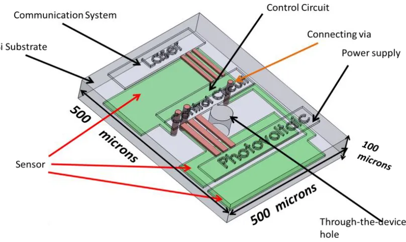
provide very sensitive and selective signals at reasonably small size scale [5]. These sensors need to be functionalized with suitable chemistry to provide selective signal for a given application. Furthermore, since the need for the small size of the system calls for easy, ideally monolithic, integration of all the subsystems, use of CMOS integrated electrochemical sensors provides this advantage automatically. Moreover, these sensors can be used for many different applications by changing their surface chemistry. This enables the use of several small scale sensors for many different sensing applications forming a true body area network[67].
Figure 15 : Proposed Design of Integrated Sensing Platform
This system shows optical powering and communication as an example. In this work, we will present our results on both optical and lower frequency electromagnetic powering and communication and compare their performances for small scale implants. This will provide a comparison into the more appropriate choice for different applications.
Summary
2.3
Integrated Sensor
Chapter 3
The sensor is defined as the component of the system which generates a signal corresponding to some physical quantity of interest. For example, a sensor is used to measure the concentration of one or more analyte of interest, usually from a mixture of many different analyte in a media e.g. body fluids (blood, interstitial fluid, etc.). There are many possible mechanisms for implementing a sensor for a particular application. The factors affecting this choice are:
• Type of analyte to be measured
• Sensitivity
• Selectivity
• Background Medium (blood, interstitial fluid, etc.)
Common sensing mechanisms utilize different means of interacting with the analyte of interest to induce a change in the response of a component or a set of components.
• Mechanical (e.g. MEMS/NEMS sensors) – Mechanical Loading of a device by analyte
• Thermodynamic (e.g. Calorimetric Sensors) – Mechanical Loading of a device by analyte
• Optical (e.g. fluorescence sensors) -- Optical Interaction with analyte
• Electrochemical– Chemical Interaction with Analyte, Electrical Output
Another electrode is used to provide a stable potential reference in the electrolyte of interest and hence is called the reference electrode (RE). The third electrode is designed to complete the cell by providing a current equal to the working electrode, but in the other direction (oxidation or reduction) and is called the counter electrode (CE) [76]. For some applications, the CE and the RE can be merged especially if the sensor current is very small. However, for stable long term operation, it is appropriate to have a separate RE to provide more stable reference which is inert (no current flow) and hence does not polarize and does not get consumed during cell operation especially if the cell reaction is not completely reversible [77]. The sensor electrodes can be planar or patterned at micro and nano scale [78]. The sensor may have some surface coatings to achieve specific performance goals. A schematic of an electrochemical sensor is shown in Figure 16.
Figure 16 : Schematic of Integrated Electrochemical Sensor
the sensors are intended for small sub-mm sized implants and the total area is limited to the size of the implant at the most. Initially, the sensor is designed assuming square dies. Later on these square CMOS dies would be shaped to other more favorable shapes for implants ( e.g. rectangular shafts or circular dies).
Electrochemical sensors work by detecting the interaction of electrolyte with the electrode surface at electrode-electrolyte interface. The interface reactions depend upon the type of current-voltage mode used in the sensor operation. There are many different modes the cell can be operated in. The most common modes are explained briefly here (details in [79]).
3.2.1.1 Potentiostatic Mode:
In this mode, the current flow at the working electrode is controlled and the resulting potential difference between the working and the reference electrode is measured. One example is keeping this current zero which results in open circuit cell potential. The potential then depends upon both electrodes’ materials as well on the electrolyte.
3.2.1.2 Amperometric Mode:
roughly an order of magnitude larger than the WE to achieve this while still keeping the sensor within our size constraints. The RE needs to be as close to the WE as possible to minimize the iR drop in the sensor (parasitic drop due to finite solution conductance). The RE size should be enough to maintain stability during the entire operation for long term implants. These constraints lead to various possible geometries. For large scale (macro) devices, optimizing the geometry is not very significant, although still relevant, since adequate performance can be achieved using many different types of geometries without any optimization. However for small scale devices it is very important to study all the factors that can affect sensor performance.
Integrated Electrochemical sensors can be fabricated on either the top or bottom of the CMOS substrate. An example of such electrochemical sensors (two different geometries) fabricated on the top metal layer of CMOS dies is shown here. The details of this fabrication process are included in methods chapter.
Figure 17 : CMOS Integrated Electrochemical Sensors
connecting these to the CMOS circuit. For example, for sensors on the back Silicon, contacts should be fabricated either using Through-Silicon vias or metal contact lines along the chip edges. Such technologies exist and can be integrated with the post-processing flow [82].
For prototyping, some example geometries were fabricated on silicon substrates as shown in Figure 18. The substrates were isolated first using thin (100nm) of either grown or deposited insulating layers (e.g. silicon oxide). The details are given in the methods chapter as well.
Figure 18 : (a) Design A (Pt RE) (b) Design M (AgCl RE) (c) Design G
(Ag RE) (d) Design N Ag (RE)
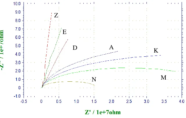
Rigorous analytical and numerical modeling methods can be used to compare these geometries for their performance. Some examples of simple numerical modeling are shown in appendix I. Experimental methods can be used as an alternative to these techniques, although testing all the possibilities can become tedious. We used a combination of modeling and experimental techniques. A few geometries were chosen based upon simulation results and their performance was compared experimentally. These were compared first using hydrogen peroxide testing to determine their sensitivity as it is the underlying sensing mechanism in most glucose sensors. The comparison of maximum sensor currents at 0.6V potential between WE and RE during a CV is shown in Figure 19.
Figure 21 : Electrochemical Impedance of sensor geometries in 20mM
Peroxide
The above results also suggest that the use of Pt RE if higher current is required as the overall cell impedance is lower in this case. This was also confirmed using impedance spectroscopy for different sensors. A typical comparison is shown in Figure 22.
Figure 22 : Impedance comparison between Ag/AgCl and Pt RE sensors
Pt RE Sensor
Ag/AgCl RE Sensor
N K
properties, the results were quite clear for multiple samples after reasonable attempts to isolate other effects like pinholes in films.
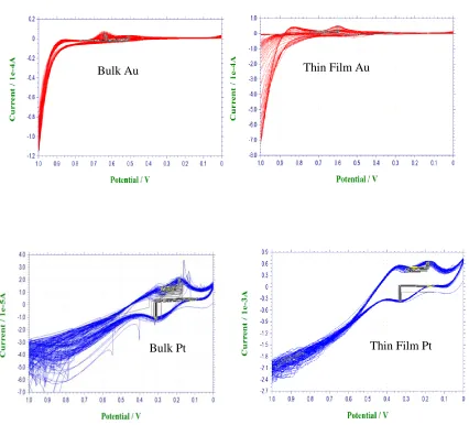
Figure 23 : Electrochemical Stability of Electrode Materials in 50mM Peroxide solution Bulk Au
elec
tro
de
Thin Film Au
electr
ode
Bulk Pt electrode
Figure 24 : Effect of Repetitive testing on electrode material (a) Au (b)
Pt
Another advantage of Pt is that direct electrochemical oxidation of glucose can occur on it at high enough potentials (around 0.6V vs. Ag/AgCl) [83]. This can be used for glucose detection with little interference rejection mechanisms. Gold, Carbon and other working electrode materials do not have this property. Although it has been reported that gold can be used in these applications, it has lower activity in amperometric mode. However, for Pulse Amperometry, it is reported to have higher activity than Pt [83]. However, in our work, we show that Pt have sufficient sensitivity which can be further increased by increasing its surface area. This, together with more long-term stability makes it more suitable as an electrode material for our applications. Hence, Pt was chosen for long-term electrochemical hydrogen peroxide sensors. For other sensing mechanisms, the comparison should be reevaluated. For example, for Nucleic Acid based sensing, it was found in the literature and in our experimental work that Au is easier to use as a working electrode material in terms of binding the nucleic acid strands (probes) using thiol bonds. The same chemistry did not show any appreciable binding to Pt. Hence, Au was chosen for such sensors as WE material.
In blood or other complex fluids, both gold and Platinum are poisoned by chloride ions and many other species (e.g. amino acids) due to surface adsorption. However, nanopatterned Pt has shown to
have high stability against these blood agents [83]. Nonetheless, since these sensors are not used in direct contact with blood, but in interstitial fluid, this is a less critical problem. For blood applications, electrodes will have to be coated with special materials for filtering (e.g. Nafion)
There are many different reference electrodes which can provide stable voltage readings in solution to form potential differences between electrodes for proper sensor operation, but the standard solid state reference electrode material is usually Ag/AgCl. Some noble metals covered with their oxide also act as pseudo-reference electrodes (e.g. Pd/PdOx, Ir/IrOx) [85]. Since we already use Pt electrodes for WE and CE, it is very desirable to test Pt-based reference electrodes and compare their performance with standard Ag/AgCl reference electrodes. The standard Ag/AgCl reference electrode is made using thin Ag deposited similar to the Pt layer. The top of this silver electrode is then converted to AgCl using different methods (dipping in strong chloride solutions, electrochemical reaction or Dry chlorine plasma) and the thickness of the AgCl layer is kept high enough for long term operation. However, not all Ag is converted into AgCl, as the sensor operation depends upon the interface between the Ag and AgCl layers[85]. The conversion was verified visually (AgCl has a brown color), spectroscopically, and through microscale structure (AgCl has a granular structure). The results of these material processing are shown in following figures.
Figure 26 : Thin Film Reference Electrode Materials (a) Ag (b)
AgCl
Figure 27 : Spectrum of Ti/Pt/Ag/AgCl electrode
Figure 28 : Thin Film Reference Electrode Materials (a) Pt (b) ‘Pt/PtOx’
Figure 29 : Spectroscopic Measurement of Pt based RE materials (a) Pt (b) PtOx
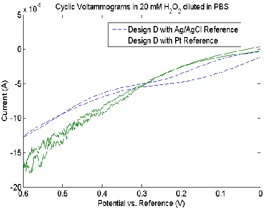
Each sensor design was fabricated with both a Pt RE and Ag/AgCl RE. The stability of the RE was tested first by measuring its potential relative to a commercial stable RE, which in our case was Ag/AgCl RE from CH instruments. Secondly, Cyclic Voltammetric measurements were performed
Pt
Si Si
Pt O
using sensors utilizing either the Ag/AgCl RE or the Pt RE. Results indicated that Ag/AgCl RE proved more stable than Pt RE especially at higher reference potentials as seen in Figure 12. This is due to interference from species reacting with Pt at such potentials, most notably hydrogen peroxide. However, it also shows that a Pt RE can still be used for less sensitive applications. Although, bare Ag showed a pretty stable response, peroxide interference had some effect on it. The formation of AgCl layer on top makes it more independent of conditions in in-vivo fluids. Also, since the chloride ion concentration in body remains pretty constant [43], the Ag/AgCl RE was used without any special concentrated coatings as are used sometimes in commercial RE. The results in PBS and other body fluids confirmed that the RE could provide good enough performance in such cases. After Chlorination, AgCl became quite stable and peroxide did not have any appreciable effect on it. Bare Pt showed more serious problems regarding stability and peroxide interference. Oxidation proved to increase stability and decrease peroxide interference effects as expected.
Ag/AgCl RE in PBS Ag/AgCl RE in peroxide Ag RE in peroxide
Figure 30 : Open Circuit Test for electrode Stability and Interference Effects
Table 1 Comparison of Different Reference Electrode’s Performance
Electrode Material Temporal Stability (voltage change)
Peroxide Interference (voltage change)
Ag 15mV 120mV
Pt 30mV 60mV
Ag/AgCl 5mV 3mV
Pt/PtOx 20mV 10mV
The open circuit potential difference between Pt/PtOx RE and AgCl RE was found to be a function of surface properties and cleanliness of the surface. There were some variations from batch to batch. However, this effect can be suppressed by standardized manufacturing and by performing some calibration with standard RE. Hence, the results suggest that a Pt based RE can be quite stable for some applications. Bare Pt itself can be used if the electrode is small and the interference from peroxide (or other similar molecules) is small. However, for very high peroxide concentrations, the Pt RE again showed interference effects. However, this occurs only at very high concentrations and
Pt RE in PBS
Pt RE in Peroxide
is only meant to demonstrate the limit of this electrode material. However, for the desired range of peroxide concentrations, this interference effect is not seen.
Figure 31 : Comparison of Pt and Ag/AgCl RE
Patterned Electrochemical Sensors
3.4
uncontrolled variation in electrode properties. If the overall size of the electrode is not large enough, this leads to significant batch-to-batch variations and hence excessive recalibration of each device is needed. Also, such patterned electrodes are susceptible to failure over long term use because of limited mechanical/chemical robustness. Finally, the methods of fabricating these electrodes are not compatible with current CMOS technologies and need specialized post-processing and extra on/off chip circuitry and equipment. Intuitively, micro scale patterning is used for species which are present in high concentrations or in bigger sizes (e.g. cells) to keep the design simple. Nano patterning is used for sensing very small concentrations or for sensing molecular species which need even smaller surface geometries to interact at molecular level [88]. However, electrode capacitance and other double layer effects need to be carefully modeled for such small scale systems to optimize the size scales for different applications. For example, Pt electrodes are known to have more capacitance than Au electrodes [89]. This means high surface area Pt electrodes should be replaced with Au electrode for fast sensing applications. Similarly, overly dense structures are not good for high frequency applications and hence micro patterning may be more useful for these applications.
Figure 32 : Nanopatterned electrochemical sensor coated with a functionalizing matrix
For electrochemical metabolic sensing, the signal changes quite slowly and capacitance is not an issue as far as the sensor speed is concerned. Generally, the smaller the size of the patterns (e.g. pillars), the larger the sensing area and the better the sensor performance. The advantage of using patterned electrodes over planar electrodes is usually depicted by the surface area enhancement as given by following equation describing surface area of a patterned electrode (S) as compared to a planar electrode (So) in hexagonal packing 2
( ) ( )
Here, r is the radius of the pillars, h is the height if the pillars and a is the separation between the pillars. For a standard rectangular arrangement of pillars, the equation can be written as
2
( ) ( )
For typical sensor parameters, the difference between the hexagonal and rectangular arrangement is not very significant. Since the rectangular arrangement is easier to layout and operate upon, we used it as the arrangement of choice in our work. These equations show that higher r/a and higher h/a give higher surface area which results in higher sensitivity and hence results in better devices. This clearly shows that electrode patterning is advantageous for performance enhancement, especially if the overall size of the sensor needs to be minimized. The exact scale of patterning depends upon the application and the cost of the processing. The height of the pillars is limited by the surface tension forces in the liquid. The pillar deflection due to these surface tension forces is given by [86]
Here, P is the capillary force, h is pillar height, E is young’s modulus and I is second moment of inertia given by
the underlying core still made of silicon. Our results confirmed that these pillars were quite robust in solutions at the size scale where other pillars are reported to have mechanical issues as reported in literature [86]. The resulting sensor with nanopatterned electrodes are shown in Figure 33. Details of the fabrication procedure are given in the methods chapter.
Figure 33 : Integrated Nanopatterned Electrochemical Sensors
The pattering methods used in this work do not need special materials, non-vacuum based processing (e.g. liquid plating methods), or complex porous templates which are difficult to replicate. This is a standard fabrication process and can even be integrated in the CMOS fabrication process to make it even more controllable and repeatable. Our novel patterning process can allow designers to design high performance electrodes for other applications apart from electrochemical electrode preparation where impedance poses a limitation.
Electrochemical Measurements
3.5
is most interesting. It also helps in finding the equivalent electrical circuit of the sensor which is required for designing the control circuit for proper sensor operation.
It is important to emphasize that EIS measurements only reflect the cell impedance at the given cell potential as is used in the experiment. Sometimes, it is very difficult to do the EIS measurements at the desired cell potential due to large signal changes happening at the interface (e.g. during electrode polarization step). Hence, EIS is done at zero bias and is used in conjunction with other methods (e.g. cyclic voltammetry) to completely characterize the system response. Also, EIS results are the aggregate impedance results and there can be many different impedance networks which can result in same EIS response. Hence, the results are normally fitted to the predicted EIS models in theory to find the value of the different components of the already known model. This fitting can be done using custom written codes or using Frequency Response Analysis (FRA) software. Since the electrochemical cell is a non-linear system, it requires the use of non-linear FRA tools and methodologies.
Figure 34 : Randles equivalent electrical model of an electrochemical cell
In this model, Cdl is the double layer capacitance at the electrode-electrolyte interface. Rct is the contact (charge transfer) resistance between the electrode and the electrolyte. Zw is the diffusion limitation (Warburg impedance) from the bulk to the electrode-electrolyte interface and Rs is the series resistance of the bulk solution between the electrodes. The double-layer capacitance is a nonlinear capacitance and hence is difficult to model. Its value depends upon many parameters including applied potential, temperature, ionic concentrations, types of ions, insulating layers, electrode roughness, impurity adsorption and so on [76]. Charge transfer resistance (Rct) is the resistance to current flow at the electrode when the electrode potential is moved away from its Nernstian value. For a given electrode with surface area A, these parameters can be calculated as
( )
| | ( )
( )
Figure 35 : Impedance Comparison between Planar and Nanopatterned Electrodes
Since the solution resistance in Randles model is the same for all the cases (the solution was PBS for all the sensors), the results clearly show that as the pillar diameter is reduced (and hence the
number of pillars is increased) the impedance of the sensor at a given frequency goes down. We also observed that both the charge transfer resistance and the double layer impedance decrease as both the real and imaginary impedances for nanopatterned electrodes are reduced with decreasing pillar diameter. The improved reduction in impedance between the electrode types is more pronounced at low frequencies which are the more critical range for most sensing mechanisms in biomedical applications. This was further confirmed by measuring the impedance difference between fully integrated planar and patterned sensors. This result confirmed the same trend for the entire sensor as was noticed for individual electrodes as shown in Figure 36.
Figure 36 : Comparison between Impedance of Planar and Patterned Sensor
For almost all measurements, the decrease in impedance due to patterning is larger than that predicted by theory. However, it is important to point out that this trend will change at very small electrode spacing due to the overlap between the electric double layers. Hence, the enhancement in overall effective surface area (electrochemical equivalent surface area) will be lower than that in
Planar Sensor
enzyme-substrate complex which then decomposes. Part of it forms product and some part goes back to the actual substrate and enzyme. In terms of chemical reactions, this can be written as
E + S ES E + P
The Michaelis-Menten constant Km is equal to the substrate concentration at which the catalytic rate is half of its maximum value. Hence the reaction rates can be described as follows
[ ]
The apparent Km is found by fitting the reaction curve (catalytic rate versus substrate concentration) to the Michaelis-Menten equation. For high enzyme activity in immobilized form, the reaction is substrate diffusion rate limited and for low activity, it is enzyme activity limited. Hence, in former case the apparent Km from curve fitting is larger than Km of free enzyme in the solution and in the latter case it is closer to the Km of free enzyme in solution under ambient conditions. For reaction rate limited by other factors (e.g. mediator concentration), the apparent Km can actually be lower than the Km of free enzyme in solution. An example of a linear fit for one of the sensors is shown in Figure 37. As seen, linear fitting of the entire curve will results in larger Km than actually measured.
k1 k2
Figure 37 : Fitting sensor response for Enzyme Kinetics
Modeling of the currents for enzyme electrodes has been performed extensively in the literature for many practical cases [100]. For the special case of thin film sensors, the current equation is modified and solved numerically. The closed form analytical solutions under some assumption is given as [101]
Here, n is number of electrons transferred in the reaction, F is faraday constant, A is electrode area,
response becomes a bit non-linear (enzyme limited region). If needed, this response can be tuned to a specific sensitivity by controlling the enzyme concentration in the immobilization matrix or by controlling the glucose flux into the immobilization layer. A typical response of a sensor coated with hydrogel with immobilized gold is shown in Figure 38. The sensor in this case consists of a planar thin film electrode as a WE using off-chip RE and CE.
Figure 38 : In vitro sensing of Glucose using electrode immobilized w/ GOx
enzymatic loading decreases with time and longer operations are possible with enzymes which can provide more sensitivity even when present in small amounts.
Figure 39 : Glucose sensing using integrated sensors with (a) GOx (b) GDH
(a)
A nanopatterned sensor with similar functionalization provided an order of magnitude improvement over these sensors as shown in Figure 40. It is good to note that the response seems similar to the simulation results of nanopatterned sensors in terms of narrow cyclic voltamograms as shown in appendix I. The sensor shows improvement over the planar sensors in many ways. It has higher current as well as higher linear region of detection. This proves that the performance of small integrated sensors can be controlled precisely by the control of their surface geometries and can be tuned to many applications where traditional planar sensors may not be able to provide sufficient performance.
Figure 40 : Nanopatterened Glucose Sensor performance
A comparison of the nanopatterned electrode with the planar electrodes provides insight into the performance enhancement provided by Nanopatterning.
0mM Glucose 1mM Glucose
3mM Glucose 5mM Glucose
Figure 41 : Comparison of Nanopatterned and Planar Sensors
Figure 42 : Chronocoulometric Sensing of Glucose in PBS
Repetitive pulsing shows that this technique is valid for ‘continuous’ measurements if the pulses are separated by a short time period. The pulses just need to be sufficiently separated to allow glucose diffusion and enzyme reaction to equilibrate completely (reach steady state) which are both pretty quick phenomenon as glucose is a small molecule and hydrogel consists mostly of water. For more detailed analysis of this system, numerical modeling using ‘transport through porous media’ can be used in the regime.
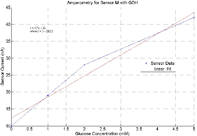
Constant potential amperometry was also used to characterize this sensor because of its potential of continuous measurement as well as less background noise compared to the Chronoamperometric and Cyclic Voltammetric methods. The WE was kept at 0.6V vs. Ag/AgCl RE for this
measurement. The results are shown in Figure 43. 0mM Glucose
1mM Glucose
2mM Glucose
Figure 43 : Amperometric Glucose Sensing using an integrated planar sensor
3.8.1 Testing in Body Fluids
Figure 44 Glucose Detection in Serum using (a) Chronoamperometry (b) CV
0mM Glucose
1mM Glucose
2mM Glucose
10mM Glucose
20mM Glucose
(a)
The sensor response in blood was even more suppressed than that in serum. This can be explained by the blockage of hydrogel sites with blood cells or other blood components. However, sensor still showed adequate sensing after couple of days of incubation as shown in Figure 44.
Figure 44 : Sensor w/GDH, test in mouse blood
As seen here, the current and sensitivity both have decreased. However, Signal processing could be used to recover sensitivity again. Furthermore, for many applications, operation in interstitial fluid can suffice, which is quite close to the serum in chemistry. Hence, direct testing in blood is not needed. If such devices are needed, some blood filtering (e.g. dialysis membranes) methods should be used to increase sensor life-time as well as to get higher signal levels for better accuracy.
0mM Glucose 3mM Glucose
6mM Glucose 10mM Glucose
.
Figure 45 : Improving Sensitivity using Signal Processing
These results show that such sensors can be used in complex body fluids. However, use of filtering mechanism can improve their response and extend their life-time for long term use.
3.8.2 Interference Issues
Interference from other species is an important concern for sensors in complex environments e.g. in vivo sensors. For glucose sensors, the most problematic interference is from acetaminophen, ascorbic acid, and urea [3]. This happens when high potentials (near 0.6V) are used for glucose sensing. The interfering species also oxidize around this potential on Pt electrodes and hence cause noise signals. As an example, a thin film Pt sensor with repeated tests in PBS shows very little deviation (noise). However, with 0.1mM Acetaminophen (AA) in the solution, the interference level increases significantly, as shown in Figure 46.
0mM 3mM
Figure 46 : Interference on Pt electrodes (a) in PBS (b) with 0.1 mM AA
Thin films of dense polymers like polyphenol (PPh) can be used to limit interference as well as immobilization of enzymes [101]. Such coatings are effective because these do not limit the smaller molecules which are being detected while filtering the larger interfering molecules. As very thin coatings (e.g. 10nm) can be very effective in interference reduction, their effect on sensing smaller molecule (like peroxide) can be negligible as shown in Figure 47. It shows that the change due to AA is negligible compared to the change due to peroxide detection. Hence, PPh acts as a very good interference rejection layer without affecting the peroxide sensing as it is much smaller molecule compared to the interfering molecules.
Figure 47 : Effect of PPh on Peroxide Detection on Pt electrode
Another method to get rid of interference is to use lower potentials or even negative potentials to keep these species from creating a signal. However, using lower positive potential for peroxide detection decreases the sensitivity, although it is still adequate for accurate detection. This method is more suitable for detecting oxygen consumption in the glucose enzymatic reaction and converting that information into oxygen concentration after adjusting for the background oxygen levels in body fluids. This approach was used in first bench top glucose sensors and is also used in some modern research due to its excellent interference rejection properties [35]. Alternatively, detection at low potentials can also be achieved if the enzymes being used can transfer the electrical charges easily to the underlying electrodes. In this case, the detection mechanism is direct charge transfer from enzyme to the underlying electrode which depends upon conduction properties of the enzyme and the immobilization matrix. For example, Glucose Dehydrogenase-FAD enzyme has a cytochrome-c entity as a part of its synthesized version from some sources [102].This entity is known to help the tunneling of electrical charge from biological molecules [103]. This can be even more pronounced
PBS
1mM AA
Glucose Oxidase based detection is known to have high sensitivity towards dissolved oxygen. This was tested by bubbling air through the solution (which increases O2 concentration as measured by a commercial dissolved oxygen sensor). Results are shown in Figure 48 and clearly indicate relatively large change due to O2 concentration change. However, secondary effects like enhanced diffusion after bubbling can also have secondary effects in such experiments.
Figure 48 : Effect of O2 bubbling on GOx Sensor
On the other hand, GDH based detection showed much reduced O2 dependence, as depicted by Figure 49. This is due to the O2 independent pathway that GDH takes for glucose oxidation.
Before Bubbling
Figure 49 : Effect of O2 bubbling on GDH Sensor
Another method to minimize interference uses multiple working electrodes to measure glucose through hydrogen peroxide and oxygen sensing mechanisms. The same enzyme can be used for this purpose along with same working electrodes. This method involves measuring at negative potentials for oxygen sensing using two electrodes, one of which is not coated with enzyme hydrogel and the other is coated with the enzyme. The difference in their oxygen measurement is proportional to the glucose concentration. Also, this does not involve interference from specie which oxidize at positive potentials and has been used for glucose sensing by itself for long time [35]. However, for very small electrodes, this may become a challenging measurement since the dissolved oxygen concentration is very small in the body fluids. Together with the hydrogen peroxide sensing mechanism, this method can generate useful results; nano-patterning of the electrodes for optimum oxygen sensing can improve dissolved oxygen sensing to make this measurement even better.
Before Bubbling
3.8.3 Lifetime and Repeatability
Longevity of these devices is crucial for meaningful implant applications. Longevity was tested by sensing for a few days to a few weeks. It was thought to provide an insight into the time response of these sensors to design appropriate calibration algorithms. Different solutions of PBS and pH buffers were added as control solutions, but did not create any appreciable change in the sensor response. This demonstrates that these sensors have very good signal to noise ratio. Also, these devices exhibit good longevity. The sensors were also measured using different hardware platforms (CHI 7051D as well as Metrohm450) and different laboratory settings to test their robustness. These were also shipped back and forth between different labs and showed very stable and repeatable results. A comparison between the sensor responses over 3 weeks is shown in Figure 50.
This test also showed that the response was not very stable. This is assumed to be a result of the functionalization matrix not completely free of unbound material. As the differences decreased with time, this argument seems quite plausible. Storing these sensors for some time before their use should decrease this effect substantially. Also, Chronocoulometric measurements showed much lower variations. We think this is because these methods are more limited by diffusion of specie rather than the gel properties. Also, larger signal and integration decreases effect of current variations somewhat.
Figure 51 : Chronocoulometric Response of a Glucose Sensor over 3
weeks
Figure 52 : Sensor to Sensor Variation within a batch
Electrochemical noise and interference (ENI) is defined as the noise due to inherent electrode processes and interference from other species due to reaction with enzyme or directly with the electrode. Noise processes on electrodes are quite complex and depend upon the type of electrode processes (Faradaic versus non-Faradaic). Thermal noise is always present in all systems and random adsorption/conduction reactions can also occur at the electrode surface. A detail of the electrochemical noise processes is given in literature [107]. A practical approach we used was to perform statistical characterization of the sensor and then use change in current (δI) as a measure of electrode noise. This change is statistical and would better model noise if a large number of measurements are taken. Also the average current (I) was used to normalize the change (δI/I) and the normalized change was found to be less than 5% in most of the cases. In these cases, the total noise of the measurement depends upon external noise sources (circuit noise, electromagnetic
0mM Glucose
2mM Glucose
noise) rather than the internal electrode noise. However, for very small sensors, the simple (δI/I) test should be repeated to see this. At some point, the electrode noise will start dominating the external noise. The clinical accuracy levels for implantable glucose levels allow 5% error. Hence, these sensors can be used for clinical applications [19].
3.8.4 Optimization of Sensor Response
Figure 53 : Effect of Nafion coating on Peroxide Detection
Another method is to again use multiple working electrodes with similar coating, but using one at a time. The electrodes can be coated with materials that degrade at a programmable rate (e.g. PLGA) and only one electrode is under use at a time. The electrodes can be switched at either a pre-programmed rate or through an external command. External sources like light, local heating, etc. can also be used for the purpose of exposing a particular electrode at one time [68].
Another optimization parameter is the choice of enzyme. The most commonly used enzyme for glucose sensing is glucose oxidase (GOx). It has been well-studied and has good sensitivity and selectivity for glucose. The most common cofactor is FAD and is the part of the enzyme (reaction center) where the glucose reaction actually happens. An issue with glucose oxidase is that it uses oxygen as a mediator for the glucose reaction. In fingerprick devices, this is overcome by using mediators. However, most of the mediators are small and toxic and are not good for implantable
PBS
6mM Peroxide
devices [37]. Glucose Dehydrogenase (GDH) is another type of enzyme which can be used for such devices. GDH with FAD cofactor is also quite sensitive and selective towards glucose. Our experiments indicated that GDH-FAD is more sensitive towards glucose than GOx and is also less sensitive to dissolved O2 concentration compared with GOx (Figure 39). It can detect smaller levels of Glucose compared with GOx which is important during hypoglycemia. It also has a wider dynamic range of detection than GOx owing to its higher activity [109]. Also, although GOx can be engineered to have an electrical transduction element, some versions of GDH-FAD naturally appears to have one [102]. The only disadvantage of GDH-FAD is that its xylose sensitivity is higher than GOx. It is reported that xylose level gets high in the body right after eating (plant based food) and it is not absorbed much, but is quickly excreted [110]. One advantage of GOx is that it has been well studied and engineered to have better stability as compared to GDH. However, with research focus on implants and hence on GDH, this difference may diminish soon. Hence, GDH-FAD appears to be the better enzyme than GOx for implantable applications. Further protein engineering can be used to decrease its xylose sensitivity and to make it even more suitable.
There are some non-enzymatic chemistries as well that are being explored for their use in glucose sensing. Boronic Acid is a common example. It has the problem of high sensitivity towards other saccharides as well [83]. Active work has been going on for improving its properties as it provides a very attractive alternative for long term applications.
hybridization, change in the nucleic acid morphology creates a change in the redox current and that change is proportional to the quantity of probes hybridized with the target. Careful surface cleaning and electrochemical profiling was done to make sure there were no redox peaks before the nucleic acid attachment. Surface properties at each step of the process were tested by electrochemical means by running a square wave voltammetry from 0 V to -0.6 V at different frequencies (near 100Hz) versus the Ag/AgCl reference electrode. Tests showed that the actual voltage of redox peak depends upon the type of the CE material as well as sensor environment and the frequency of detection. For sensors with Au CE, the peak position seems to be a bit shifted (from the redox potential of the methylene blue probe) towards the higher potential. The peak was also more broadened than the sensors with Pt CE. The peak position appears to be a function of frequency for Au CE sensors, but not for Pt CE sensors as shown in Figure 54.This demonstrates that Pt or other noble metals should be used as CE material for these sensors. Also, control of surface morphology at each step is very important for a successful sensor based upon surface chemistry.
Figure 54 : Frequency Dependence of MB Redox Peak 30 Hz
60 Hz
30 Hz
The difference in the peak current corresponds to the decrease in redox current of the methylene blue probe which corresponds to change in the morphology of the probe strand due to hybridization.
3.9.3 Results

![Figure 2 : Effect of discrete diabetes management events on personal health [9]](https://thumb-us.123doks.com/thumbv2/123dok_us/1056822.1131978/28.612.179.472.344.550/figure-effect-discrete-diabetes-management-events-personal-health.webp)