University of South Florida
Scholar Commons
Graduate Theses and Dissertations Graduate School4-7-2016
Design Exploration and Application of Reversible
Circuits in Emerging Technologies
Saurabh Kotiyal
University of South Florida, [email protected]
Follow this and additional works at:http://scholarcommons.usf.edu/etd
Part of theComputer Engineering Commons, and theComputer Sciences Commons
This Thesis is brought to you for free and open access by the Graduate School at Scholar Commons. It has been accepted for inclusion in Graduate Theses and Dissertations by an authorized administrator of Scholar Commons. For more information, please [email protected].
Scholar Commons Citation
Kotiyal, Saurabh, "Design Exploration and Application of Reversible Circuits in Emerging Technologies" (2016).Graduate Theses and Dissertations.
Design Exploration and Application of Reversible Circuits in Emerging Technologies
by
Saurabh Kotiyal
A dissertation submitted in partial fulfillment of the requirements for the degree of
Doctor of Philosophy
Department of Computer Science and Engineering College of Engineering
University of South Florida
Major Professor: Nagarajan Ranganathan, Ph.D. Srinivas Katkoori, Ph.D. Sanjukta Bhanja, Ph.D. Kandethody Ramachandran, Ph.D. Hao Zheng, Ph.D. Date of Approval: March 22, 2016
Keywords: Reversible logic, Optical Computing, Quantum cost, Ancilla inputs
DEDICATION
ACKNOWLEDGMENTS
I would like to thank my advisor Dr. Nagarajan Ranganathan for providing me the op-portunity for pursuing my research. As a mentor, Dr. Ranganathan has been instrumental in shaping my research career. I would always be thankful for his encouragement and constant support during the difficult times and showing confidence in me during those times. His valuable inputs and suggestions have a great influence on my research career, which resulted in transforming me into a better researcher. I would like to thank Dr. Himanshu Thapliyal for all of his valuable advices and suggestions throughout the years. I would also like to thank Dr. Srinivas Katkoori, Dr. Hao Zheng, Dr. Sanjukta Bhanja and Dr. Kandethody Ramachandran for taking the time to be in my doctoral committee and providing valuable suggestions to improve this manuscript. I am extremely grateful to the CSE department faculties, Dr.Rangachar Kasturi, Dr. Swaroop Ghosh, Dr. Dmitry Goldgof and Dr. Larry Hall, and CSE department staff for all their help and support.
TABLE OF CONTENTS LIST OF TABLES iv LIST OF FIGURES vi ABSTRACT x CHAPTER 1 INTRODUCTION 1 1.1 Motivation 3 1.2 Contributions of Dissertation 7 1.3 Outline of Dissertation 10
CHAPTER 2 BACKGROUND AND RELATED WORK 12
2.1 Reversible Logic Gates 12
2.1.1 Controlled-V and Controlled-V+ Gate 12
2.1.2 The NOT Gate 13
2.1.3 Feynman Gate (CNOT Gate) 14
2.1.4 Fredkin Gate 15
2.1.5 Toffoli Gate 16
2.1.6 Peres Gate 17
2.2 Background on Mach-Zehnder Interferometer (MZI) Based
Optical Reversible Computing 18
2.2.1 All Optical Feynman Gate 19
2.2.2 Mach-Zehnder Interferometer (MZI) Based 3x3
Tof-foli Gate 20
2.2.3 Mach-Zehnder Interferometer (MZI) Based 3x3 Peres
Gate 21
2.3 Background on Linear Optical Quantum Computing 23
2.3.1 Linear Optical Quantum 3x3 Toffoli Gate 24
CHAPTER 3 MACH-ZEHNDER INTERFEROMETER BASED DESIGN OF ALL
OPTICAL REVERSIBLE BINARY ADDER 27
3.1 Proposed All Optical Reversible Gates 28
3.2 Proposed All Optical Reversible Ripple Carry Adder with
3.2.1 Steps of Proposed Methodology for Optical Reversible
Adder 33
3.2.2 Theorem for Proposed Methodology of Optical
Re-versible Adder 35
3.2.3 Proof of Theorem for Proposed Methodology of
Op-tical Reversible Adder 35
3.3 Delay and Optical Cost Analysis 36
3.3.1 Comparison of n Bit Optical Reversible Ripple Carry Adders 37
3.4 Conclusion 38
CHAPTER 4 EFFICIENT REVERSIBLE NOR GATES AND THEIR MAPPING
IN OPTICAL COMPUTING DOMAIN 40
4.1 All Optical Reversible NAND Gates 41
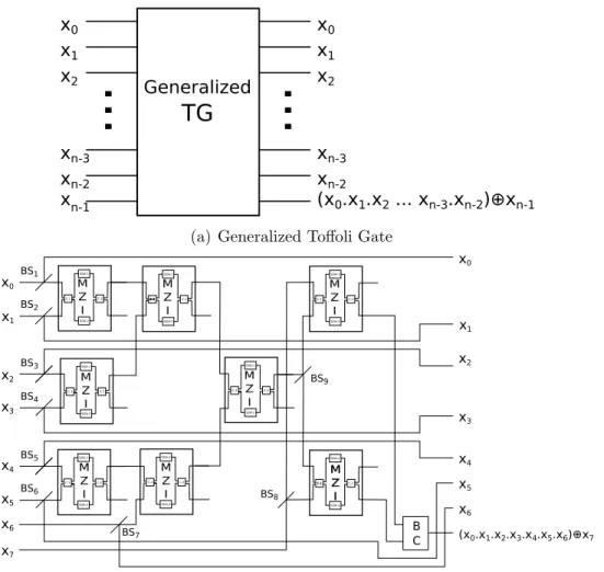
4.1.1 MZI Based Generalized Toffoli Gate (GTG) 41
4.1.2 Generalized Linear Optical Quantum Computing Based
Reversible Toffoli Gate 42
4.2 Proposed NOR Logic Based Reversible Gates and Their
Map-ping in Optical Domain 43
4.2.1 Proposed Generalized Reversible NOR Gate for MZI Mapping 43 4.2.2 Proposed Linear Optical Quantum Computing Based
Reversible NOR Gate (LOQC-RNOR) 45
4.2.3 Proposed Generalized Linear Optical Quantum
Com-puting Based Reversible NOR Gate 49
4.3 Comparison of Proposed NOR Logic Based Reversible Gates
with NAND Logic Based Reversible Gates Mapped in Optical Domain 51
4.3.1 Comparison of 3-Input and 3-Output Gates 51
4.3.2 Comparison of n-Input and n-Output Mach-Zehnder
Interferometer Based Reversible Logic Gates 52
4.3.3 Comparison of Proposed Reversible NOR Gate (LOQC-RNOR) with Existing Toffoli Gate Mapped in Linear
Optical Quantum Computing Domain 54
4.4 Discussion and Conclusions 55
CHAPTER 5 DESIGN OF REVERSIBLE ADDER-SUBTRACTOR AND ITS
MAP-PING IN OPTICAL COMPUTING DOMAIN 57
5.1 Design of Unified Optical Reversible Adder-Subtractor 57 5.1.1 Design of Optical Reversible Adder-Subtractor Based
on Approach 1 58
5.1.2 Design of Optical Reversible Adder-Subtractor Based
on Approach 2 58
5.2 Comparison of n Bit Reversible Adder-Subtractor 59
CHAPTER 6 REVERSIBLE LOGIC BASED MULTIPLICATION COMPUTING
UNIT USING BINARY TREE DATA STRUCTURE 65
6.1 Proposed Binary Tree-Based Design Methodology for NxN
Reversible Multiplier 65
6.2 Design Example of a 4x4 Bit Reversible Multiplier Based on
Proposed Methodology 70
6.3 Comparison of Proposed Reversible Multiplier Design with
Existing Designs 74
6.3.1 Comparison Study with Reversible Array Multipliers 76 6.4 Proposed Binary Tree-Based Design Methodology for Signed
NxN Reversible Multiplier 78
6.5 Design Example of a Signed 5x5 Reversible Multiplier Based
on Proposed Design Methodology 79
6.5.1 Comparison of Proposed Signed 5x5 Reversible
Mul-tiplier Design with Existing Designs 86
6.6 Comparison of Proposed Signed Reversible Multiplier Design
with Existing Designs 87
6.7 Conclusion 90
CHAPTER 7 LIMITATIONS AND CONCLUSION 91
REFERENCES 93
APPENDIX A: COPYRIGHT PERMISSIONS 102
LIST OF TABLES
Table 1.1 Truth Table of Conventional and Reversible XOR Gates 2 Table 1.2 Ancilla Inputs and Garbage Outputs of a NxN Reversible
Array Multiplier 7
Table 2.1 Truth Table of Toffoli-Sign Gate 25
Table 2.2 Truth Table of Linear Optical Quantum 3x3 Toffoli Gate 26
Table 3.1 Truth Table of Optical Reversible Gate I (ORG-I) 30
Table 3.2 Truth Table of Optical Reversible Gate II (ORG-II) 30 Table 3.3 Optical Cost and Delay of All Optical Implementation of
Reversible Gates 37
Table 3.4 A Comparison of Reversible Ripple Carry Adder with Input
Carry 38
Table 3.5 Optical Cost Comparison of Reversible Ripple Carry Adders
(with Input Carry) 38
Table 3.6 Delay (in ∆) Comparison of Reversible Ripple Carry Adders
(with Input Carry) 39
Table 4.1 Truth Table of All Optical 3x3 MZI-RNOR Gate 46
Table 4.2 Truth Table for Linear Optical Quantum Computing Based
3x3 Reversible NOR Gate (LOQC-RNOR) 49
Table 4.3 Optical Cost and Delay of 3x3 Reversible NAND Logic Gate
and Proposed 3x3 MZI-RNOR Gate Mapped In MZI Switch 52 Table 4.4 Optical Cost and Delay Analysis of 3x3 Reversible Logic
Gates by Implementing 13 Standard Boolean Functions 53 Table 4.5 Optical Cost and Delay Analysis of All Optical nxn
Re-versible NOR Logic Gates by Implementing 13 Standard
Table 5.1 A Comparison of The Proposed Reversible Adder-Subtractor 60 Table 5.2 A Comparison of Reversible Adder-Subtractor Based on
Ap-proach 2 62
Table 5.3 Optical Cost Comparison of Reversible Adder-Subtractor
Based on Approach 2 63
Table 5.4 Delay (in ∆) Comparison of Reversible Adder-Subtractor
Based on Approach 2 63
Table 6.1 A Comparison of 4x4 Reversible Multiplier 74
Table 6.2 A Comparison of NxN Reversible Multipliers 77
Table 6.3 A Comparison of Signed Reversible Multipliers 87
LIST OF FIGURES
Figure 1.1 Conventional and Reversible XOR Gates 2
Figure 1.2 Ancilla Inputs of Reversible Array Multiplier 7
Figure 1.3 Garbage Outputs of Reversible Array Multiplier 8
Figure 2.1 Controlled-V and Controlled-V+ Gate 13
Figure 2.2 NOT Gate 13
Figure 2.3 Feynman Gate (CNOT Gate), Its Quantum Implementation
and Useful Properties 14
Figure 2.4 Fredkin Gate and Its Quantum Implementation 15
Figure 2.5 Toffoli Gate and Its Quantum Representation 16
Figure 2.6 Peres Gate and Its Quantum Implementation 17
Figure 2.7 Mach-Zehnder Interferometer (MZI) Based All Optical Switch 18
Figure 2.8 Feynman Gate and Its All Optical Implementation 20
Figure 2.9 3x3 Toffoli Gate and Its MZI Based Optical Implementation (TG: Toffoli Gate, MZI: Mach-Zehnder Interferometer, BC:
Beam Combiner, BS: Beam Splitter) 21
Figure 2.10 Peres Gate and Its All Optical Implementation (PG: Peres Gate, MZI: Mach-Zehnder Interferometer, BC: Beam
Com-biner, BS: Beam Splitter) 22
Figure 2.11 Qubit and Qutrit in Linear Optical Quantum Computing 23 Figure 2.12 Linear Optical Quantum Logic Gates and Unitary Matrix
Representation 23
Figure 2.13 A Linear Optical Quantum Toffoli-Sign Gate 24
Figure 3.1 All Optical Implementations of Optical Reversible Gate I
(ORG-I) and Optical Reversible Gate II (ORG-II) 29
Figure 3.2 Optical Reversible Gate I (ORG-I) and Optical Reversible
Gate II (ORG-II) 29
Figure 3.3 Graphical Representation of Proposed Optical Reversible
Gates and Design of An Optical Reversible Full Adder 31 Figure 3.4 Circuit Generation of Optical Reversible n Bit Adder Using
Proposed Optical Reversible Gate I (ORG-I) and Optical
Reversible Gate II (ORG-II) 32
Figure 3.5 Proposed Optical Reversible 4 Bit Adder 34
Figure 4.1 Generalized Toffoli Gate and Its MZI Based Optical Imple-mentation (TG: Toffoli Gate, MZI: Mach-Zehnder
Interfer-ometer, BC: Beam Combiner, BS: Beam Splitter) 42
Figure 4.2 Generalized Linear Optical Quantum Computing Based
Re-versible Toffoli Gate 43
Figure 4.3 Generalized MZI-RNOR Gate and Its MZI Based Optical Implementation (MZI-RNORG: MZI-RNOR Gate, MZI: Mach-Zehnder Interferometer, BC: Beam Combiner, BS: Beam
Splitter) 45
Figure 4.4 3x3 MZI-RNOR Gate and Its MZI Based Optical Imple-mentation (MZI: Mach-Zehnder Interferometer, BC: Beam
Combiner, BS: Beam Splitter) 47
Figure 4.5 Linear Optical Quantum Computing Based 3x3 Reversible
NOR Gate (LOQC-RNOR) 48
Figure 4.6 A Linear Optical Quantum Computing, Based Reversible
NOR Gate (LOQC-RNOR) 49
Figure 4.7 Transformation of The Proposed Linear Optical Quantum Computing Based Reversible NOR Gate (LOQC-RNOR) for Control Signal Values (|C2, C1 >=|0,0>)
* No Transformations are Performed at Stage (c) and (e),
as Controlled-NOR Gate Has C1 =|0>as Control Value 50
Figure 4.8 Generalized Linear Optical Quantum Computing Based
Figure 4.9 Three-Control-Qubit Linear Optical Quantum LOQC-RNOR and Toffoli Gate (* Here Xb Gate Swaps The State|1>and
|3 >, While The Xa Gate Swaps The Information Between
State|0>and|2>; The Target Is a Four Level Information
Carrier) 55
Figure 4.10 Comparison of Number of Linear Optical Quantum Gates Required in Proposed LOQC-RNOR Gate Versus Toffoli
Gate for Various Values of Number of Qubits 56
Figure 5.1 Proposed Optical Reversible n Bit Adder-Subtractor Based
on Approach 1 59
Figure 5.2 Proposed Optical Reversible n Bit Adder-Subtractor Based
on The Optical Ripple Carry Adder with Input Carry 60 Figure 5.3 Proposed Optical Reversible n Bit Adder-Subtractor Based
on Approach 2 61
Figure 5.4 Proposed Optical Reversible n Bit Adder-Subtractor Based
on The Optical Ripple Carry Adder with Input Carry 62 Figure 6.1 A Binary Tree Representation of a NxN Reversible
Multi-plier (p: Partial Products; ps: Partial Sums; S: Final Sum) 67 Figure 6.2 A N-Bit Reversible Partial Product Generation Circuit (G0
to G2n−1: Garbage Outputs) 68
Figure 6.3 Addition of Partial Products for a 4x4 Multiplication (c10,c20:
Carry Outs) 69
Figure 6.4 A Binary Tree Representation of a 4x4 Reversible Multiplier 70 Figure 6.5 Proposed 4x4 Reversible Multiplier Design Using Reversible
Ripple Adders (G0 toG13: Garbage Outputs; S0 toS8: Final Result) 72
Figure 6.6 A 4x4 Reversible Multiplier Design Using Reversible Ripple Adders with Input Carry (G0 to G21: Garbage Outputs; P0
to P8: Final Result) 73
Figure 6.7 % Improvement of The Proposed Reversible Multiplier
Com-pared to Existing Reversible Array Multiplier 77
Figure 6.8 Addition of Partial Products for a Signed 4x4 Multiplication
Figure 6.9 A Partial Product Generation Circuit for Signed NxN
Re-versible Multiplier (G0 toG2n−1: Garbage Outputs) 81
Figure 6.10 Addition of Partial Products for a Signed 5x5 Multiplication
(c10,c20,c30: Carry Outs) 82
Figure 6.11 A Binary Tree Representation of a Signed 5x5 Reversible Multiplier 83 Figure 6.12 Proposed Signed 5X5 Reversible Multiplier Design Using
Reversible Ripple Adder (P0 to P10: Final Result; G0 to
G22: Garbage Outputs) 84
Figure 6.13 A Partial Product Generation Circuit for Signed 5x5 Re-versible Multiplier (G0 to G9: Garbage Outputs; p0 to p24:
Partial Products) 84
Figure 6.14 A Signed 5x5 Reversible Multiplier Design Using Reversible Ripple Carry Adders with Input Carry (P0 to P10: Final
Result; G10 to G32: Garbage Outputs; p0 to p24: Partial
Products) 85
Figure 6.15 Improvement of The Proposed Signed Reversible Multiplier
ABSTRACT
The reversible logic has promising applications in emerging computing paradigms, such as quantum computing, quantum dot cellular automata, optical computing, etc. In re-versible logic gates, there is a unique one-to-one mapping between the inputs and outputs. To generate a useful gate function, the reversible gates require some constant ancillary in-puts called ancilla inin-puts. Also to maintain the reversibility of the circuits some additional unused outputs are required that are referred to as the garbage outputs. The number of ancilla inputs, the number of garbage outputs and quantum cost plays an important role in the evaluation of reversible circuits. Thus minimizing these parameters are important for designing an efficient reversible circuit. Reversible circuits are of highest interest in optical computing, quantum dot cellular automata and quantum computing. The quantum gates perform an elementary unitary operation on one, two or more two-state quantum systems called qubits. Any unitary operation is reversible in nature, and hence, quantum networks are also reversible, to conclude the quantum computers must be built from reversible logic components.
The main contribution of this dissertation is the design exploration and application of reversible circuits in emerging nanotechnologies. The emerging technologies explored in this work are 1) Optical quantum computing 2) Quantum computing.
The first contribution of this dissertation is Mach-Zehnder interferometer based design of all optical reversible binary adder. The all optical reversible adder design is based on two new optical reversible gates referred as optical reversible gate I (ORG-I) and optical re-versible gate II (ORG-II) and the existing all optical Feynman gate. The two new rere-versible
gates ORG-I and ORGI-II have been proposed and can implement a reversible adder with a reduced optical cost which is equal to the number of MZI switches required, less propagation delay, and with zero overhead in terms of number of ancilla inputs and the garbage outputs. The proposed all optical reversible adder design based on the ORG-I and ORG-II reversible gates are compared and shown to be better than the other existing designs of reversible adder proposed in the non-optical domain in terms of number of MZI switches, delay, the number of ancilla inputs and the garbage outputs. The proposed all optical reversible adder will be a key component of an all optical reversible arithmetic logical unit (ALU), that is a quite essential component in a wide variety of optical signal processing applications. In the existing literature, the NAND logic based implementation is the only known implementation available for reversible gates and its functions. There is a lack of research in the direction of NOR logic based implementation of reversible gates and functions. The second contribution of this dissertation is the design of NOR logic based n-input and n-output reversible gates, one of which can be efficiently mapped into optical computing using the Mach-Zehnder in-terferometer (MZI), while the other can be mapped efficiently in optical computing using the linear optical quantum gates. The proposed reversible NOR gates work as a corresponding NOR counterpart of NAND logic based Toffoli gates. The proposed optical reversible NOR logic gates can implement the reversible boolean logic functions with less number of linear optical quantum logic gates with reduced optical cost and propagation delay compared to the implementation using existing optical reversible NAND gates. It is illustrated that an optical reversible gate library having both optical Toffoli gate and the proposed optical re-versible NOR gate is superior compared to the library containing only the optical Toffoli gate: (i) in terms of number of linear optical quantum gates when implemented using linear optical quantum computing (LOQC), (ii) in terms of optical cost and delay when imple-mented using the Mach-Zehnder interferometer. The third contribution of this dissertation is a binary tree-based design methodology for a NxN reversible multiplier. The proposed
binary tree-based design methodology for a NxN reversible multiplier performs the addition of partial products in parallel using the reversible ripple adders with zero ancilla bit and zero garbage bit; thereby, minimizing the number of ancilla and garbage bits used in the design. The proposed design methodology shows improvements in terms of number of ancilla inputs and garbage outputs compared to all the existing reversible multiplier designs. The methodology is also extended to the design of NxN reversible signed multiplier based on modified Baugh-Wooley multiplication methodology.
CHAPTER 1
INTRODUCTION
Reversible logic is a logic design style in which there is a one to one mapping between the input and the output vectors. According to [1], if a system is irreversible in nature then erasing a bit causes kTln2 joules of heat energy to be dissipated, where k is the Boltzmann’s constant and T is the absolute temperature of the environment. This kTln2 joule of heat energy won’t be dissipated, if a computation is performed reversibly based on reversible logic circuits [2]. The reversible logic has extensive applications in emerging technologies such as quantum computing, quantum dot cellular automata, optical computing, etc. [3, 4]. The major application of reversible logic lies in quantum computing. A quantum computer will be viewed as a quantum network (or a family of quantum networks) composed of quantum logic gates; each gate is performing an elementary unitary operation on one, two or more two-state quantum systems called qubits. Quantum networks must be built from reversible logical components [5].
The input and output vector of an N-input and N-output reversible logic gate or N XN
reversible logic gate can be represented as:
Iu = I1, I2, I3, ..., IN (1.1)
Ou = O1, O2, O3, ..., ON (1.2)
Here Iu and Ou represents the input and output vectors of a reversible logic gate. The
conventional CMOS logic gates are irreversible in nature as the input vectors can not be regenerated directly by the output vectors. Thus erasing a bit or loss of information causes
kTln2 joules of heat energy [1] to be dissipated. However in reversible logic gates, there exists a unique one to one mapping between the input and output vectors. An irreversible XOR gate can be represented as shown in Fig. 1.1(a), where A, B and P are the inputs and outputs respectively.
A
B
P=A⊕B (a) Conventional XOR Gate
A B P=A Q=A⊕B Reversible XOR
(b) Reversible XOR Gate
Figure 1.1. Conventional and Reversible XOR Gates
In the conventional XOR gate, the inputs A and B are mapped to the output P as
P = A⊕B. Whereas in the reversible logic, an XOR gate can be represented as shown in Fig. 1.1(b), where A, B and P, Q are the input and outputs respectively. Here the mapping between the inputs and outputs can be represented as P =A and Q=A⊕B and holds the property of unique input and output vector mapping property of reversibility. The reconstruction of input vectors from the output vectors can be seen in table 1.1(b). The table 1.1(a) shows the input and output vectors for a conventional XOR gate. In the table 1.1(a) it can be seen that for the output P = 0 the input vectors are AB = 01,10, whereas in the table 1.1(b) each output vector corresponds to a unique input vector.
Table 1.1. Truth Table of Conventional and Reversible XOR Gates
(a) Conventional XOR Gate
A B P =A⊕B
0 0 0
0 1 1
1 0 1
1 1 0
(b) Reversible XOR Gate
A B P =A Q=A⊕B
0 0 0 0
0 1 0 1
1 0 1 1
1.1 Motivation
The emerging technologies such as Quantum computing, quantum dot cellular automata (QCA), optical quantum computing has promising applications for reversible logic [5, 6, 4, 7, 8]. The reversible logic satisfies the quantum computing property of unique one to one mapping between the input and output vectors. It has been proven by the researchers that, if a computation is performed in an irreversible manner then the loss of each bit of information produces kTln2 Joules of heat energy [1]. In order to avoid this limit, from a thermodynamics point of view, Bennett proved that kTln2 joules of heat energy would not be dissipated if the computation is carried in a reversible manner [2]. Thus, from thermodynamic considerations, a firm lower limit on dissipation of Ediss =kT ln2≈ 18meV
(in room-temperature environment) is a necessity for conventional (irreversible) logic, even if reliability issues could be ignored. If the physical implementation of the logic can be physically reversible, in that case, reversible logic can be useful for designing non-dissipative circuits. The current CMOS technology can be considered as a practical implementation platform for implementing reversible circuits as CMOS is not physically reversible. In CMOS, the energy of a signal can be characterized as Esig=(1/2) CV2, here energy is directly
proportional the voltage change and is much higher than the kTln2 limit.
In contrary, there exists emerging nanotechnologies such as Optical Computing, Quan-tum Cellular Automata (QCA) and Superconducting Flux Logic (SFL) family, etc., where the energy dissipation due the loss of information will be a significant factor of overall heat dissipation of the system [9, 10, 11, 12, 13, 14, 15]. Thus, in this dissertation our primary motivation for adopting reversible logic lies in the fact that, it can provide a logic design terminology for creating ultra-low power circuits beyond the limit of kTln2, that are ap-plicable for the emerging nanotechnologies in which the energy dissipated due to the loss of information will be significant factor of the overall heat dissipation. For an example, in
Superconductor Flux Logic (SFL) family based nSQUID gates, the energy dissipation in conventionally logically irreversible design is close to few kTln2 per logic operation. Here by employing reversible at 4 K temperature, the energy dissipation per nSQUID gate per bit is measured below the thermodynamics limit of kTln2 [11]. Therefore, the reversible logic has been extensively investigated for its promising application in power-efficient nanocomputing [16, 17, 18].
A photon can provide unmatched high speed and can store the information in a signal of zero mass. These properties of photon have attracted the attention of researchers to implement the reversible logic gates in all optical domain. The optical implementation of reversible logic gates could be useful to overcome the limits imposed by conventional computing, and is also considered as an implementation platform for quantum computing [19, 20, 21, 22, 23, 24, 25, 26, 27, 28]. In the existing literature there are two types of optical mapping of reversible logic gates: (i) based on the semiconductor optical amplifier (SOA) using the MachZehnder interferometer (MZI) switch [29, 4, 30]; (ii) based on linear optical quantum computation (LOQC) using linear optical quantum logic gates [23, 24, 25, 26, 27, 28]. In recent years, researchers have implemented several reversible logic gates in optical computing domain such as Feynman gate, Toffoli gate, Peres gate, Modified Fredkin gate and reversible NOR gates [29, 4, 30]. The optical implementation of reversible logic gates can be achieved using SOA-based MZI optical switches. The MZI-based implementation of reversible logic gates provides significant advantages such as high speed, low power, fast switching time.
In the existing literature, the most widely used implementation of reversible logic gates and the reversible boolean functions are the implementations using NAND logic. This is due to the lack of research in the direction of NOR logic based reversible logic gates and func-tions. In this work, we propose two NOR logic based n-input and n-output reversible gates one of which can be efficiently mapped in optical computing using the MachZehnder
inter-ferometer (MZI) while the other one can be mapped efficiently in optical computing using the linear optical quantum gates. The first reversible NOR gate is called as a MachZehnder interferometer based reversible NOR gate (MZI-RNOR), and the second reversible NOR gate is called as a linear optical quantum computing based reversible NOR gate (LOQC-RNOR). The proposed optical reversible NOR gates are useful for NOR logic based implementation of reversible boolean functions. The proposed MZI-RNOR gate can implement the reversible boolean functions with reduced optical cost and propagation delay compared to the im-plementation of reversible boolean functions using optical reversible NAND gates (NAND logic based reversible gates is all optical Toffoli gate) implemented using the MZI switch. The proposed LOQC-RNOR can implement the reversible boolean functions with a reduced number of linear optical quantum logic gates compared to the implementation of reversible boolean functions implemented using linear optical quantum reversible NAND gates (NAND logic based reversible gates is linear optical quantum Toffoli gate). As the proposed optical reversible NOR gates are n-input and n-output optical reversible NOR-based counterpart of NAND logic based n-input and n-output Toffoli gate, thus we have also illustrated the optical design of the n-input and n-output Toffoli gate. In this work, the optical cost of a reversible logic gate is defined as the number of MZI switches used in its all optical implementation [31]. We illustrated the advantages of proposed optical reversible NOR gates in terms of optical cost and delay by implementing the 13 standard boolean functions [32]. The 13 stan-dard boolean functions proposed in [23] can represent all possible 256 combinations of three variable boolean functions. It is illustrated that an optical reversible gate library having both optical Toffoli gate and the proposed optical reversible NOR gate is superior compared to the library containing only the optical Toffoli gate: (i) in terms of number of linear optical quantum gates when implemented using linear optical quantum computing (LOQC) and (ii) in terms of optical cost and delay when implemented using the MachZehnder interferometer.
Further in the field of quantum computing, researchers have proposed the design of reversible array multiplier [33]. The array multiplier approach is based on the following two steps: 1) generate the partial products using the reversible partial product generation circuitry 2) perform the addition of partial products generated at step one using the array of reversible full adders and reversible half adders. In this work, we are assuming that step one which is responsible for the generation of partial product using the reversible partial product generation circuitry will be the same for all multipliers. A NxN reversible partial
product generation circuitry requires N2 ancilla inputs and generates 2N garbage outputs.
The details of step one will be discussed in section 6.1. In the reversible array multiplier,
the step two which requires the addition of partial products would need an N reversible half adders and (N2 −2N) reversible full adders. In the existing literature, Peres gate
can work as a reversible half adder with one ancilla input and one garbage output. The design of reversible full adder will need one ancilla input and two garbage outputs. Thus, to design an NxN reversible array multiplier (without considering the ancilla inputs and garbage outputs of reversible partial product generation circuitry), the number of ancilla inputs can be computed as AN = (N + (N2−2∗N)) and the number of garbage outputs
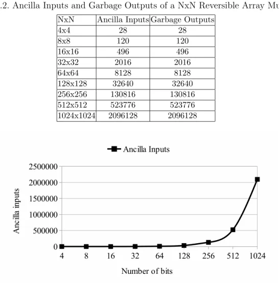
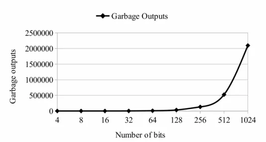
can be computed asGO = (N+ 2(N2−2∗N)). Table 1.2 shows the number of ancilla inputs
and garbage outputs in NxN reversible multiplier for various values of N (including reversible partial product generation circuitry). Figures 1.2 and 1.3 show the plot of ancilla inputs and garbage outputs in NxN reversible multiplier for various values of N. From Figures 1.2 and 1.3, it is very evident that the number of ancilla inputs and garbage outputs in NxN reversible array-based multiplier increases exponentially with N. This sets our main objective to design a new reversible multiplier based on binary tree architecture that is primarily optimized in terms of the number of ancilla inputs and garbage outputs. The details of our proposed binary tree-based reversible multiplier will be discussed in section 6.1.
Table 1.2. Ancilla Inputs and Garbage Outputs of a NxN Reversible Array Multiplier
NxN Ancilla Inputs Garbage Outputs
4x4 28 28 8x8 120 120 16x16 496 496 32x32 2016 2016 64x64 8128 8128 128x128 32640 32640 256x256 130816 130816 512x512 523776 523776 1024x1024 2096128 2096128
Figure 1.2. Ancilla Inputs of Reversible Array Multiplier
1.2 Contributions of Dissertation
The key parameters to design an efficient reversible logic design are as follows:
• Reducing the number of constant input bits, also referred as the ancilla inputs
• Minimizing the number of garbage outputs
Figure 1.3. Garbage Outputs of Reversible Array Multiplier
• Minimizing the cost of the circuit, here the cost is measured in terms of the number of 1x1 and 2x2 quantum gates required to design a circuit
While keeping above mentioned parameters in consideration, we have proposed efficient reversible logic design methodologies targeting different emerging nanotechnologies. The dis-sertation presents the following contributions towards the design exploration and application of reversible circuits in emerging technologies.
• The first contribution of this dissertation is the all optical implementation of an n bit reversible ripple carry adder for the first time in literature. The all optical reversible adder design is based on two new optical reversible gates referred as optical reversible gate I (ORG-I) and optical reversible gate II (ORG-II) and the existing all optical Feynman gate. The two new reversible gates ORG-I and ORG-II are proposed as they can implement a reversible adder with a reduced optical cost which is the measure of number of MZIs switches and the propagation delay, and with zero overhead in terms of number of ancilla inputs and the garbage outputs. The proposed all optical reversible adder design based on the ORG-I and ORG-II reversible gates are compared
and shown to be better than the other existing designs of reversible adder proposed in the non-optical domain in terms of number of MZIs, delay, the number of ancilla inputs and the garbage outputs. The proposed all optical reversible ripple carry adder will be a key component of an all optical reversible ALU that can be applied in a wide variety of optical signal processing applications.
• The second contribution is proposing two NOR logic based n-input and n-output re-versible gates one of which can be efficiently mapped in optical computing using the Mach-Zehnder interferometer (MZI) while the other one can be mapped efficiently in optical computing using the linear optical quantum gates. The proposed reversible NOR gates work as a corresponding NOR counterpart of NAND logic based Toffoli gates. The proposed optical reversible NOR logic gates can implement the reversible boolean logic functions with reduced number of linear optical quantum logic gates or reduced optical cost and propagation delay compared to their implementation using existing optical reversible NAND gates. It is illustrated that an optical reversible gate library having both optical Toffoli gate and the proposed optical reversible NOR gate is superior compared to the library containing only the optical Toffoli gate: (i) in terms of number of linear optical quantum gates when implemented using linear optical quan-tum computing (LOQC), (ii) in terms of optical cost and delay when implemented using the Mach-Zehnder interferometer.
• The third contribution of this dissertation is presenting a binary tree-based design methodology for a NxN reversible multiplier. The proposed binary tree-based design methodology for NxN reversible multiplier performs the addition of partial products in parallel using the reversible ripple adders with zero ancilla bit and zero garbage bit; thereby minimizing the number of ancilla and garbage bits used in the design. The proposed design methodology shows a 17.86% to 60.34% improvement in terms of
ancilla inputs, and 21.43% to 52.17% in terms of garbage outputs compared to all the existing reversible multiplier designs. The methodology is also extended to the design of NxN reversible signed multiplier based on modified Baugh-Wooley multiplication methodology.
• The other important contribution of this dissertation is proposing two design method-ologies of reversible adder-subtractor to optimize the parameters of ancilla input bits, the number of garbage outputs, optical cost, and the delay. The proposed efficient design of optical reversible adder-subtractor will find promising applications in opti-cal reversible computing and could form a key component of optiopti-cal reversible digital processing circuits and architectures.
1.3 Outline of Dissertation
The organization of the dissertation is as follows: Chapter 1 provides the introduction to the proposed work. It also provides a brief review of quantum computing and reversible computing. The Chapter 2 provides the background and related work towards this proposed dissertation work. In this chapter, a brief review of reversible logic gates, Mach-Zehnder Interferometer (MZI) and Linear Optical Quantum Computing (LOQC) have been provided. In Chapter 3, the details on proposed Mech-Zehnder Interferometer based design of all optical reversible binary adder have been provided. A detailed delay and optical cost based analysis is also provided for proposed Mech-Zehnder Interferometer based design of all optical reversible binary adder. Chapter 4 presents the design of efficient reversible NOR gates and their mapping in optical computing domain. A comparison of proposed NOR logic based reversible gates with NAND logic based reversible gates is also provided in this chapter. The Chapter 5 provides details on the design of reversible adder-subtractor and its mapping
in optical computing domain. In Chapter 6, we have proposed the reversible logic based multiplication computing unit using binary tree data structure.
CHAPTER 2
BACKGROUND AND RELATED WORK
2.1 Reversible Logic Gates
In the existing literature, there exists several reversible gates such as the Feynman gate, Toffoli gate, and the Fredkin gate. The quantum cost of a reversible gate is the number of 1x1 and 2x2 reversible gates required to design a 3x3 reversible gate. The quantum cost of all 1x1 and 2x2 reversible gates are considered as unity [34, 35, 36]. The 3x3 reversible gates are implemented using the 1x1 NOT gate and 2x2 reversible gates such as Controlled-V and Controlled-V+ (V is a square-root of the NOT gate, and V+ is its hermitian), and the Feynman gate is also known as Controlled NOT gate (CNOT).
2.1.1 Controlled-V and Controlled-V+ Gate
A controlled-V gate is shown in Fig. 2.1(a). In a controlled-V gate, when the value of control signal A=0, then the qubit B will pass through the controlled part unchanged, i.e., we will have Q=B. When the value of control signal A=1, then the unitary operation
V = i+12 −1i−1i is applied to input B, i.e., Q=V(B). The controlled-V+ gate is shown in
Fig. 2.1(b). In the controlled-V+ gate when the value of control signal A=0, then the
qubit B will pass through the controlled part unchanged, i.e., we will have Q=B. When the value of control signal A=1, then the unitary operationV+ =V−1 is applied to the input B, i.e.,Q=V+(B).
(a) Controlled-V Gate (b) Controlled-V+Gate
Figure 2.1. Controlled-V and Controlled-V+ Gate The V and V+ quantum gates have the following properties:
V ×V =N OT
V ×V+ =V+×V =I
V+×V+ =N OT
The property, as shown above, represents that, when two V gates are in series they will behave as an NOT gate. Similarly twoV+ gate in series behaves as an NOT gate. A V gate in series with a V+ gate and vice versa forms an identity. The more details on V and V+
gate and its properties can be found in [5, 35].
2.1.2 The NOT Gate
An NOT gate is 1x1 gate represented as shown in Fig. 2.2. Since it is a 1x1 gate, its quantum cost is unity.
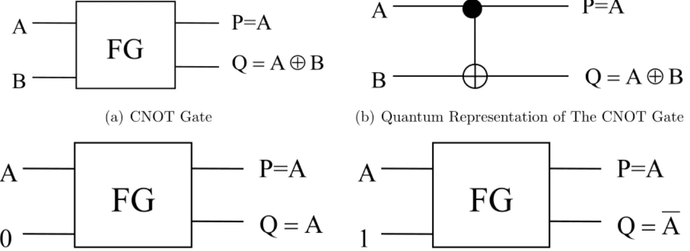
2.1.3 Feynman Gate (CNOT Gate)
The Feynman gate (FG) also known as the controlled-NOT gate (CNOT) is a 2-inputs and 2-outputs reversible gate with the mapping (A, B) to (P=A, Q=A⊕B). Here A is the controlling input and B is the controlled input; P and Q are the two outputs of the gate. Since the Feynman gate is a 2x2 reversible gate, it has a quantum cost of 1. Figure 2.3(a) and 2.3(b) shows the block representation and equivalent quantum representation of the Feynman gate. The fanout is not allowed in a reversible logic-based design. Feynman gate is very helpful in this regard as it can be used for copying the signal thus avoiding the fanout issue in reversible logic-based design as shown in Fig. 2.3(c). The Feynman gate can also be used for generating the complement of a given input signal as shown in Fig. 2.3(d).
(a) CNOT Gate (b) Quantum Representation of The CNOT Gate
(c) Feynman Gate for Avoiding The Fanout (d) Feynman Gate for Generating The
Comple-ment of a Signal
Figure 2.3. Feynman Gate (CNOT Gate), Its Quantum Implementation and Useful Proper-ties
2.1.4 Fredkin Gate
The Fredkin gate is a 3x3 reversible logic gate, with three inputs and three outputs. Figure 2.4(a) shows the block representation of a Fredkin gate. The Fredkin gate maps inputs (A, B, C) to outputs (P=A, Q= ¯AB+AC,R =AB+ ¯AC ), where A, B, C are the inputs and P, Q, R are the outputs, respectively [37].
(a) Fredkin Gate
(b) Quantum Representation of The Fredkin Gate
Figure 2.4. Fredkin Gate and Its Quantum Implementation
A Fredkin gate can work as 2:1 MUX, as it can swap its other two inputs (B, C) depending on the value of its first input (A). Referring to the Fig. 2.4(a), the first input A works as a controlling input while the inputs B and C works as controlled inputs. Thus, when A=1 the inputs B and C will be swapped and results in the value of outputs as Q=C and R=B. For the value of controlling input A=0, the outputs P and Q will be directly connected to inputs A and B. Figure 2.4(b) shows the quantum implementation of a Fredkin gate with a quantum cost of 5 [35]. In Fig. 2.4(b) each dotted rectangle is equivalent to a 2x2 Feynman gate, and
the quantum cost of each dotted rectangle is considered as 1 [34]. The same assumption is used for calculating the quantum cost of the Fredkin gate in [35]. Thus, the quantum cost of a Fredkin gate is 5 as it consists of 2 dotted rectangles, 1 Controlled-V gate, and 2 CNOT gates. In this work, we have also followed the assumption by [34], and in our quantum cost calculations, the quantum cost of the Fredkin gate is considered as 5.
2.1.5 Toffoli Gate
The Toffoli gate (TG) is a 3X3 reversible logic gate with three inputs and three outputs. The inputs to outputs mapping of a Toffoli gate can be represented as (A,B,C) to (P =A,
Q=B,R =A.B⊕c), where A, B, C are the inputs and P, Q, R are the outputs of a Toffoli gate. Figure 2.5(a) shows the block diagram of a Toffoli gate.
Toffoli Gate A B C P=A Q=B R=A.B⊕C
(a) Toffoli Gate
(b) Quantum Representation of The Toffoli Gate
A Toffoli gate has a quantum cost of 5, as it can be implemented using 2 V gates, 1 V+
gate and 2 CNOT gates [38]. Figure 2.5(b) shows the quantum implementation of a Toffoli gate using V gates, V+ gate and CNOT gates.
2.1.6 Peres Gate
The Peres gate is a 3X3 reversible gate with a mapping between the inputs A, B, C and the outputs P, Q, R as (A, B, C) to (P = A, Q = A⊕b, R = A.B ⊕C) [39]. A block representation of the Peres gate is shown in Fig. 2.6(a) and Fig. 2.6(b) shows the quantum representation of the Peres gate. The quantum implementation of Peres gate requires 2 V+
gates, 1 V gate and 1 CNOT gate. Thus, the quantum cost of a Peres gate can be calculated as 4. Peres Gate A B C P=A Q=A⊕B R=A.B⊕C
(a) Peres Gate
(b) Quantum Representation of The Peres Gate
2.2 Background on Mach-Zehnder Interferometer (MZI) Based Optical Re-versible Computing
In recent years, the Mach-Zehnder interferometer (MZI) based optical switch has drawn the interest of many researchers in the field of all optical reversible logic [4, 29, 30, 40]. A design of all optical MZI switch is shown in Fig. 2.7(a). An MZI based all optical switch can be designed using 2 Semiconductor optical amplifier (SOA-1, SOA-2) and two couplers(C-1, C-2). The operating principle of MZI based all optical switch can be explained as follows:
In Mach-Zehnder Interferometer (MZI), there are two input ports A and B and two output ports called as bar port and cross port, respectively as shown in Fig.2.7(a). At the input ports, the optical signal coming from port B is considered as the control signal (λ2)
and the optical signal coming from port A is considered as the incoming signal ( λ1).
SOA-1 SOA-2 C-1 C-2 (Incoming Signal(λ1)) A B (Control Signal (λ2)) A.B(Bar Port) A.B(Cross Port)
(a) Semiconductor Optical Amplifier Based Mach-Zehnder Interferometer (MZI)
M
Z
I
A
B
A.B
A.B
(b) Mach-Zehnder InterferometerThe working of the MZI can be explained as follows: (i) When there is an incoming signal at port A and the control signal at port B then there is a light present at the output bar port and there is no light present at the output cross port (ii) In the absence of control signal at input port B and incoming signal at input port A, then the outputs of MZI are switched and results in the presence of light at the output cross port and no light at the bar port. In our work, we have considered no light or absence of light as the binary value 0. The above behavior of MZI based all optical switch can be represented as boolean functions having inputs to outputs mapping as (A, B) to (P=AB, Q = AB¯), where A (incoming signal), B (control signal) are the inputs of Mach-Zehnder Interferometer (MZI) and P (Bar Port), Q (Cross Port) are the outputs of Mach-Zehnder Interferometer (MZI), respectively. A block representation of MZI based all optical switch is shown in Fig. 2.7(b). In our work the optical cost and the delay (∆) of MZI based all optical switch is considered as a unity.
2.2.1 All Optical Feynman Gate
The Feynman gate (FG) is a 2 inputs and 2 outputs reversible gate. It has the mapping (A, B) to (P=A, Q= A ⊕ B) where A, B are the inputs and P, Q are the outputs, respec-tively. The Feynman is also referred as the Controlled-Not gate (CNOT), as for the value of controlled input A=1 the output generated at Q will be the complement of input B that is Q= ¯B. A Feynman gate can be implemented using 2 MZI based all optical switches, 2 beam combiners (BC) and 2 beam splitters (BS) in all optical reversible computing [4]. The beam combiner (BC) simply combines the optical beams, while the beam splitter simply splits the optical beams into two optical beams. Hence, researchers do not consider them in the optical cost and the delay calculation in all optical quantum computing domain [41, 42]. Figure 2.8(a) and 2.8(b) shows the block representation and the all optical implementation of the Feynman gate. From the Fig. 2.8, it can be seen that the Feynman gate can be implemented using 2 MZI based optical switches. Hence, the optical cost of Feynman gate is
considered as 2. In the all optical implementation of the Feynman gate, two MZIs switches works in parallel thus the delay of the optical Feynman gate is considered as 1 ∆.
(a) Feynman Gate
P=A
M
Z
I
M
Z
I
BS1 B C B C B A Q=A⊕B BS2 BS3(b) All Optical Implementation of The Feynman Gate
Figure 2.8. Feynman Gate and Its All Optical Implementation
2.2.2 Mach-Zehnder Interferometer (MZI) Based 3x3 Toffoli Gate
Toffoli gate is the most popular universal reversible gate, as it can function as an NAND gate. Consider a 3-input and 3-output Toffoli gate referred as TG in Fig. 2.9(a). The inputs to outputs mapping of a 3x3 TG is (A,B,C) to (P =A, Q=B,R =A.B⊕C), where A, B, C are the inputs and P, Q, R are the outputs, respectively [4]. When C=1, the outputs of the Toffoli gate transform as P =A,Q=B, R=A.B⊕1 = A.B.
Figure 2.9(b) represents the Toffoli gate working as an NAND gate when the value of input signal C is set to one. An all optical 3x3 Toffoli gate can be implemented using 3 MZI based all optical switches, 1 beam combiner (BC) and 4 beam splitters [4]. Figure 2.9(a) and Fig. 2.9(c) shows the block representation and all optical implementation of Toffoli gate, respectively. The optical cost of the Toffoli gate is considered as 3, as the Toffoli gate can
TG
Q=B P=A AC R=A.B⊕C
B
(a) 3x3 Toffoli Gate
TG
Q=BP=A A
1 R=A.B
B
(b) NAND Gate Implementation Using 3x3 Toffoli Gate P=A R=AB⊕C
M
Z
I
M
Z
I
M
Z
I
BS1 BS2 B C A B C BS4 BS3 Q=B(c) MZI Based Optical Implementation of The 3x3 Toffoli Gate
Figure 2.9. 3x3 Toffoli Gate and Its MZI Based Optical Implementation (TG: Toffoli Gate, MZI: Mach-Zehnder Interferometer, BC: Beam Combiner, BS: Beam Splitter)
be implemented using 3 MZI based all optical switches. The Toffoli gate has a delay of 2∆, as two MZI switches out of three MZI switches works in parallel. Following the above idea of 3x3 Toffoli gate, it can be easily followed that a generalized n-inputs and n-outputs Toffoli
gate can work as an n-1 input NAND gate by hard wiring the value of last input as 1.
2.2.3 Mach-Zehnder Interferometer (MZI) Based 3x3 Peres Gate
The Peres gate is a 3x3 reversible logic gate with the inputs to outputs mapping as (A,
are the outputs respectively [30]. An all optical Peres gate can be implemented using 4 MZI based switches, 5 beam splitters (BS) and 3 beam combiners (BC). Figure 2.10(a) and Fig. 2.10(b) shows the block representation and the all optical implementation of a Peres gate, respectively. The optical cost of Peres gate is 4, as the all optical implementation of Peres gate requires 4 MZI based switches. The delay of a Peres gate is 2∆, as two MZI switches work in parallel with the two other MZI switches.
PG
Q=A⊕BP=A A
C R=A.B⊕C
B
(a) Peres gate
P=A Q=A⊕B R=AB⊕C M Z I M Z I M Z I M Z I BS1 BS2 B C B C B C A B C BS5 BS3 BS4
(b) All optical implementation of the Peres gate
Figure 2.10. Peres Gate and Its All Optical Implementation (PG: Peres Gate, MZI: Mach-Zehnder Interferometer, BC: Beam Combiner, BS: Beam Splitter)
2.3 Background on Linear Optical Quantum Computing
The linear optical quantum computing uses the photons to encode the information. The information stored in the linear optical quantum computer are in the form of qubits and qutrits. A qubit has two possible logical states referred as |0> and |1>, while a qutrit has three logical states represented as |0>, |1>, |2>. The representation of a qubit and qutrit in linear optical quantum computing is shown in Fig. 2.11.
Figure 2.11. Qubit and Qutrit in Linear Optical Quantum Computing
(a) Controlled-Z Gate (b) Controlled-NOT Gate
(c) Hadamard Gate (d) NOT Gate (X) (e) Xa Gate
The basic linear optical quantum logic gates that perform the logical operation on the qubits and qutrits are NOT gate, Hadamard gate, Xa gate, Controlled-NOT (CNOT) gate
and Controlled-Z gate. Figure 2.12 shows the linear optical quantum logic gates and their respective unitary matrix representation.
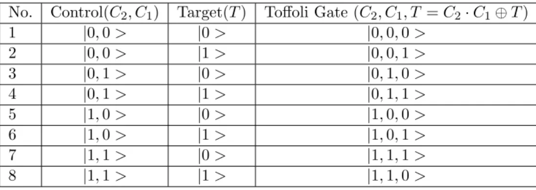
2.3.1 Linear Optical Quantum 3x3 Toffoli Gate
In the existing literature, the researchers have proposed the implementation of 3x3 Toffoli gate in linear optics quantum computing [26, 27, 28]. The existing design of a linear optical quantum 3x3 Toffoli gate is based on the design of a linear optical quantum Toffoli-sign gate. The linear optical quantum Toffoli-sign gate is a three-qubit quantum gate that imposes a sign shift to one of the logical states based on the values of two control signals or qubits [26, 27, 28]. An implementation of a linear optical quantum Toffoli-sign gate using the three two-qubit gates is shown in Fig. 2.13.
Figure 2.13. A Linear Optical Quantum Toffoli-Sign Gate
The linear optical quantum implementation of the Toffoli-sign gate has the target bit as a qutrit with the logical states as |0 >, |1 >, |2 >. The linear optical quantum logic gate represented asXain Fig.2.13 works on a qutrit and performs the swap operation between the
logic state —0¿ and —2¿, this gate leaves the logic state —1¿ unchanged. The unitary matrix of the quantum logic gate Xa is shown in Fig. 2.12. The unitary matrix of the Hadamard
gate and the controlled-Z gate used in the linear optical quantum implementation of Toffoli-sign gate is also shown in Fig. 2.12. The truth Table of the inputs to outputs mapping of a Toffoli-sign gate is shown in Table 2.1. From Table 2.1 it can be seen that the Toffoli-sign gate performs a sign shift only for the input state |C2, C1, T >=|1,0,1>.
Table 2.1. Truth Table of Toffoli-Sign Gate
No. Control(C2, C1) Target(T) Toffoli-Sign Gate (C2, C1, T)
1 |0,0> |0> |0,0,0> 2 |0,0> |1> |0,0,1> 3 |0,1> |0> |0,1,0> 4 |0,1> |1> |0,1,1> 5 |1,0> |0> |1,0,0> 6 |1,0> |1> −|1,0,1> 7 |1,1> |0> |1,1,0> 8 |1,1> |1> |1,1,1>
A linear optical quantum Toffoli gate can be implemented using the Toffoli-sign gate by applying two additional Hadamard gates before and after the target qutrit and by applying additional two NOT gate (X gates) before and after second control qubit (C1) as shown in
Fig. 2.14 [26, 27, 28].
Figure 2.14. A Linear Optical Quantum Toffoli Gate
The truth table representation of the linear optical quantum Toffoli gate using the Toffoli-sign gate is shown in Table 2.2. From Table 2.2, it can be seen that the linear optical quantum Toffoli gate performs a bit flip on the target qutrit only for the input state|C2, C1 >=|1,1>.
two-qubit gates (2 CNOT gates and 1 Controlled-Z gate) and 6 one-two-qubit gates (2 Xa gates, 2
Hadamard gates and 2 NOT gates (X gates)).
Table 2.2. Truth Table of Linear Optical Quantum 3x3 Toffoli Gate
No. Control(C2, C1) Target(T) Toffoli Gate (C2, C1, T =C2·C1⊕T)
1 |0,0> |0> |0,0,0> 2 |0,0> |1> |0,0,1> 3 |0,1> |0> |0,1,0> 4 |0,1> |1> |0,1,1> 5 |1,0> |0> |1,0,0> 6 |1,0> |1> |1,0,1> 7 |1,1> |0> |1,1,1> 8 |1,1> |1> |1,1,0>
CHAPTER 3
MACH-ZEHNDER INTERFEROMETER BASED DESIGN OF ALL
OPTICAL REVERSIBLE BINARY ADDER
1 Optical implementation of reversible logic gates is gaining the attention of researchers
as a photon can provide the unmatched high speed and can have the information stored in a signal of zero mass. Reversible logic gates implemented in optical computing can be useful to overcome the limits imposed by conventional computing with minimal energy dissipation, and is also considered one of the feasible alternatives to implement quantum computing [20, 19, 21, 22]. Recently, researchers have also implemented reversible logic gates such as Feynman gate, Toffoli gate, Peres gate and Modified Fredkin gate using semiconductor optical amplifier (SOA)-based Mach-Zehnder interferometer (MZI) optical switch due to its significant advantages such as high speed, low power, fast switching time and ease in fabrication [29, 4, 30]. In this work, we present the all optical implementation of an n bit reversible ripple carry adder for the first time in literature. The all optical reversible adder design is based on two new optical reversible gates referred as optical reversible gate I (ORG-I) and optical reversible gate II (ORG-I(ORG-I) and the existing all optical Feynman gate. The two new reversible gates ORG-I and ORG-II are proposed as they can implement a reversible adder with a reduced optical cost which is the measure of number of MZIs switches and the propagation delay, and with zero overhead in terms of number of ancilla inputs and the
1Portions of this chapter were published in the Design Automation Test in Europe Conference Exhibition
garbage outputs. In any reversible circuit, the ancilla inputs and the garbage outputs are considered as overhead and need to be minimized, as more the number of ancilla inputs and the garbage outputs more will be the number of the I/O pins in the circuit [43]. The proposed all optical reversible adder design based on the ORG-I and ORGII reversible gates are compared and shown to be better than the other existing designs of reversible adder proposed in the non-optical domain in terms of number of MZIs, delay, number of ancilla inputs and the garbage outputs. The proposed all optical reversible ripple carry adder will be useful to design an all optical reversible ALU that can be applied in a wide variety of optical signal processing applications.
3.1 Proposed All Optical Reversible Gates
In this work, we propose two new optical reversible gates that are most efficient to design an all optical reversible ripple carry adder with input carry. The proposed all optical reversible gates are referred as optical reversible gate I (ORG-I) and optical reversible gate II (ORG-II). The block representation of optical reversible gate I and optical reversible gate II are shown in Fig. 3.2(a) and 3.2(b), respectively. The optical reversible gate I (ORG-I) is a 3 inputs and 3 outputs reversible gate with mapping of inputs (A, B, C) to outputs as (P = AB + (A⊕B)C, Q = A⊕B, R = AB¯ + (A⊕B)C). The optical implementation of ORG-I is shown in Fig. 3.1(a) using 3 MZI based optical switch (MZI), 4 beam splitters (BS) and 3 beam combiners (BC). The optical reversible gate II is a 3 inputs and 3 outputs reversible gate with mapping between the inputs (A, B, C) and outputs (P, Q, R) as (A, B, C) to (P =AB¯+BC, Q= ¯BC + ¯AB, R =AB+ ¯BC). The optical implementation of an ORG-II is shown in Fig. 3.1(b) using 3 MZI based switches (MZI), 4 beam splitters (BS) and 3 beam combiners (BC). The truth table representation of optical reversible gate I and optical reversible gate II are shown in Tables 3.1 and 3.2, respectively. As the cost of an all optical reversible logic gate is the number of MZI based optical switches, hence the optical
cost of ORG-I and ORG-II will be considered as 3. In ORG-I out of 3 MZI switches, 2 MZI switches work in parallel. Thus, its delay is considered as 2 ∆. The optical implementation of ORG-II has all three MZI based optical switches working in parallel, thus has a delay of 1 ∆. Q=A⊕B P=AB+(A⊕B)C M Z I M Z I B A C R=AB+(A⊕B)C BS2 BS1 B C M Z I B C B C BS3 BS4
(a) All optical Implementation of Optical Reversible Gate I (ORG-I)
P=AB+BC Q=BC+AB M Z I M Z I B C B C B A C R=AB+BC M Z I B C BS4 BS3 BS2 BS1
(b) All optical Implementation of Optical Reversible Gate II (ORG-II)
Figure 3.1. All Optical Implementations of Optical Reversible Gate I (ORG-I) and Optical Reversible Gate II (ORG-II)
A B ORG-I C Q=A⊕B P=AB+(A⊕B)C R=AB+(A⊕B)C
(a) Optical Reversible Gate I (ORG-I) A B ORG-II C P=AB+BC Q=BC+AB R=AB+BC (b) Optical Reversible Gate II (ORG-II)
Figure 3.2. Optical Reversible Gate I (ORG-I) and Optical Reversible Gate II (ORG-II) The graphical representation of optical reversible gate I (ORG-I) and optical reversible gate II (ORG-II) are shown in Figs. 3.3(a) and 3.3(b). As the proposed gates are new and
Table 3.1. Truth Table of Optical Reversible Gate I (ORG-I) A B C AB+ (A⊕B)C A⊕B AB¯+ (A⊕B)C 0 0 0 0 0 0 0 0 1 0 0 1 0 1 0 0 1 0 0 1 1 1 1 0 1 0 0 0 1 1 1 0 1 1 1 1 1 1 0 1 0 0 1 1 1 1 0 1
Table 3.2. Truth Table of Optical Reversible Gate II (ORG-II)
A B C AB¯+BC BC¯ + ¯AB AB+ ¯BC 0 0 0 0 0 0 0 0 1 0 1 1 0 1 0 0 1 0 0 1 1 1 1 0 1 0 0 1 0 0 1 0 1 1 1 1 1 1 0 0 0 1 1 1 1 1 0 1
perform unique boolean operations thus, we have used three different geometries(triangle, pentagon, square) for their graphical representation. It is to be noted that these geometries are simply used to distinguish ORG-I and ORG-II from other existing optical reversible gates and hence provides a unique graphical representation. An important property of optical reversible gate I (ORG-I) and optical reversible gate II (ORG-II) is when the outputs of optical reversible gate I is connected to the inputs of optical reversible gate II in series it results in a 1-bit optical full adder design. This property is illustrated in Fig. 3.3(c) which shows that the proposed gates can implement an optical 1-bit reversible full adder with the optical cost of 6 and delay of 3 ∆.
A
B
C
Q=A⊕B
P=AB+(A⊕B)C
R=AB+(A⊕B)C
(a) Graphical Representation of Optical Reversible Gate IA
B
C
P=AB+BC
Q=BC+AB
R=AB+BC
(b) Graphical Representation of Optical Reversible Gate II
C
inA
B
R(C
out)=C
inP=A
Q(Sum)=A⊕B⊕C
(c) Optical Reversible Full Adder Design Using Proposed Gates
Figure 3.3. Graphical Representation of Proposed Optical Reversible Gates and Design of An Optical Reversible Full Adder
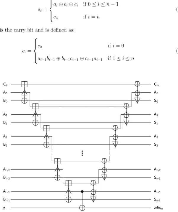
3.2 Proposed All Optical Reversible Ripple Carry Adder with Input Carry
The optical reversible ripple carry adder with input carry (c0) is designed without any
ancilla inputs and the garbage outputs, and with less optical cost and reduced delay compared to the existing non-optical reversible ripple carry adder design approaches [44, 45, 46]. The comparison is done with non-optical reversible ripple carry adders as the proposed work of the design of optical reversible adder is the first attempt in the direction of implementing reversible adder in optical computing. Consider the addition of two n bit numbers ai andbi
stored at memory locationsAi andBi, respectively, where 0≤i≤n−1. The input carryc0
is stored at memory location A−1. Further, consider that memory locationAn is initialized
with z∈ {0, 1}. At the end of the computation, the memory location Bi will havesi, while
the locationAi keeps the valueai for 0≤i≤n−1. Further, at the end of the computation,
the additional locationAn that initially stores the value z will have the valuez⊕sn, and the
bit reversible ripple carry adder). Thus An will have the value of sn when z=0. Here, si is
the sum bit produced and is defined as:
si = ai ⊕bi⊕ci if 0≤i≤n−1 cn if i=n (3.1)
where ci is the carry bit and is defined as:
ci = c0 if i= 0 ai−1bi−1⊕bi−1ci−1⊕ci−1ai−1 if 1≤i≤n (3.2) A0 B0 Cin A1 B1 A2 B2 An-2 Bn-2 An-1 Bn-1 A0 S0 Cin A1 S1 A2 S2 An-2 Sn-2 An-1 Sn-1 z⊕sn z
Figure 3.4. Circuit Generation of Optical Reversible n Bit Adder Using Proposed Optical Reversible Gate I (ORG-I) and Optical Reversible Gate II (ORG-II)
The generalized methodology of designing the n bit optical reversible ripple carry adder with input carry is shown in Fig. 3.4. The methodology is explained below along with an illustrative example of 4-bit optical reversible ripple carry adder. The illustrative example of 4 bit all optical reversible ripple carry adder is shown in Fig. 3.5 that can perform the addition of two 4 bit numbersa=a0...a3 andb=b0...b3, and has the input carryc0. The details
of the proposed approach that uses optical reversible gate I (ORG-I) and optical reversible gate II (ORG-II) along with Feynman gates to minimize the optical cost and the delay with zero overhead in terms of garbage outputs and the ancilla inputs is discussed below.
3.2.1 Steps of Proposed Methodology for Optical Reversible Adder
• Step 1 has the following two sub-steps:
• For i=0 to n-1: At a pair of locations, Ai, Bi and Ci apply the optical reversible
gate I (ORG-I) gate such that the location Ai anBi are passed to the inputs A,
B respectively, of the optical reversible gate I (ORG-I).
For i=0 the input carry Cin is passed to the input C0 of optical reversible gate
I, while for the value of i=1 to n-1 the input carry is propagated in the circuit. The propagated input carry is generated at the location Ai of optical reversible
gate I in the circuit and passed to location Ci for i=1 to n-1 as Ci=Ai−1. The
inputAi is transformed to AiBi+ (Ai⊕Bi)Ci and is passed to the input Ci+1 as
propagated carry. So in our case the value ofCi+1=Ai for i=1 to n-1. The input
Bi is transformed as Ai⊕Bi and input Ci is transformed as AiB¯i+ (Ai⊕Bi)Ci.
• Further for i=n: apply the optical Feynman gate at pair of locationsAn−1, An.
• For i=n-1 to 0:
such that the locationAi anBi are passed to the inputs A, B respectively, of the optical
reversible gate II (ORG-II).
a0 b0 c0 a1 b1 a2 b2 a3 b3 a0b0+(a0⊕b0)c0=c1 a0⊕b0 a0b0+(a0⊕b0)c0 z a1b1+(a1⊕b1)c1=c2 a1⊕b1 a1b1+(a1⊕b1)c1 a2b2+(a2⊕b2)c2=c3 a2⊕b2 a2b2+(a2⊕b2)c2 a3b3+(a3⊕b3)c3=s4 a3⊕b3 a3b3+(a3⊕b3)c3 z⊕s4 a3 s3=a3⊕b3⊕c3 c3 a2 s2=a2⊕b2⊕c2 c2 a1 s1=a1⊕b1⊕c1 c1 a0 s0=a0⊕b0⊕c0 c0 Step 1 Step 2 z⊕s4
Figure 3.5. Proposed Optical Reversible 4 Bit Adder
For i=n-1 the propagated input carry Cn−1 generated from previous step from optical
reversible gate I is passed to the input Cn−1 of optical reversible gate II, while for the
value of i=n-2 to 0 the input carry is propagated further in the circuit. The propagated input carry is generated at the location Ai of optical reversible gate II in the circuit
and passed to location Ci for i=n-1 to 0 as Ci = Ai+1. The input Ai is transformed
to AiB¯i +BiCi and is passed to the input Ci−1 as propagated carry for i=n-1 to 0.
So in our case the value of Ci−1 can be represented as Ai for i=n-1 to 0. The input
Bi is transformed as ¯BiCi + ¯AiBi and inputCi is transformed as AiBi+ ¯BiCi. After
this step we will have the complete working design of the optical reversible adder an example of which is shown for addition of 4 bit numbers in Fig.3.5.
3.2.2 Theorem for Proposed Methodology of Optical Reversible Adder
Let a and b are two n bit binary numbers represented as ai and bi, c0 is the input carry
(c0), and z ∈ {0, 1} is the another 1 bit input, where 0 ≤ i ≤ n−1, then the proposed
design steps of methodology result in the ripple carry adder circuit that works correctly. The proposed design methodology designs an n bit adder circuit that produces the sum output
si at the memory location where bi is initially stored while the location where ai is initially
stored is restored to the value ai for 0 ≤ i ≤ n−1. Further, the memory location where z
is initially stored transforms to z⊕sn, and the memory location where the input carry c0 is
initially stored is restored to the value c0.
3.2.3 Proof of Theorem for Proposed Methodology of Optical Reversible Adder
The proposed approach will make the following changes on the inputs that are illustrated as follows:
• Step 1: The step 1 of the proposed approach transforms the inputAi,Bi andCi states
to n−1 O i=0 |aibi+ (ai ⊕bi)cii|ai⊕bii|aib¯i+ (ai⊕bi)cii ! |z⊕sni
where fori= 0, ci =cin else ci =ai−1.
For illustrative purpose, the transformation of the input states of a 4 bit all optical reversible adder circuit after step 1 is shown in Fig.3.5.
• Step 2: The step 2 of the proposed approach transforms the input states to
n−1 O i=0 |aii |sii ! |c0i |z⊕sni
For illustrative purpose, the transformation of the input states of a 4 bit all optical reversible adder circuit after step 2 is shown in Fig.3.5.
Thus, we can see that the proposed two-step will produce the sum output si at the
memory location where bi is stored initially while the location where ai is stored initially
will be restored to the value ai for 0 ≤ i ≤ n−1. The memory location where z is stored
will have z⊕sn and the memory location where the input carry c0 was stored initially will
be restored to the value c0. This proves the correctness of the proposed methodology of
designing the all optical reversible ripple carry adder with input carry.
3.3 Delay and Optical Cost Analysis
The proposed optical reversible ripple carry adder with input carry can be designed by following the two steps described previously. The delay and optical cost analysis of the proposed adder are performed by analyzing the steps involved in the design of all optical reversible ripple carry adder with input carry.
• Step 1 of the proposed methodology requiresn optical reversible gate I (ORG-I), that works in series thus in this step the proposed design of all optical reversible adder will have the optical cost of 3n and delay of 2n∆. Step 1.b has a CNOT gate that is used to generate the carry out, and it contributes the optical cost of 1 and delay of 1∆. Thus, the total optical cost of Step 1 is 3n+ 1 and delay of 2n+ 1∆
• Step 2 of the proposed methodology requires n optical reversible gate II (ORG-II) working in series thus in this step the proposed design of all optical reversible adder will have the optical cost of 3n and delay of n∆.
The total optical cost of the proposed optical reversible ripple carry adder with input carry can be summed up as 3n+ 1 + 3n = 6n+ 1. The propagation delay of the proposed design will be (2n+ 1)∆ +n∆ = (3n+ 1)∆.
3.3.1 Comparison of n Bit Optical Reversible Ripple Carry Adders
There are various existing non-optical reversible designs of n bit ripple carry adders in the literature such as the design in [44, 45, 46]. Thus, we are summarizing the optical cost and the delay of the various reversible gates used in the existing work in Table 3.3. The optical cost and the delay summarized in Table 3.3 will be used for comparison of the proposed design of the optical reversible n bit adder with the existing non-optical reversible n bit adders. The Table 3.4 illustrates the comparison of the proposed design with the existing designs proposed in [44, 45, 46].
Table 3.3. Optical Cost and Delay of All Optical Implementation of Reversible Gates Optical Cost Delay
Feynman Gate [4] 2 1∆
Fredkin Gate 2 1∆
Peres Gate [30] 4 2∆
Toffoli Gate [4] 3 2∆
TR Gate 4 2∆
The Table 3.4 shows that the proposed optical design of the reversible n bit adder excels the existing non-optical reversible designs of n bit adder in terms of optical cost and delay and have zero overhead in terms of number of ancilla inputs and the garbage outputs. From Table 3.5 it can be seen that the proposed design of the optical reversible carry adder achieves the improvement ratios ranging from 12.50% to 24.91%, 63.97% to 66.65%, 60.80% to 66.63% and 66.67% to 68.41% compared to the designs presented in designs of [45, 44, 46] in terms of optical cost. From Table 3.6, it can be seen that the proposed design of optical reversible ripple carry adder achieves the improvement ratios ranging from 0.03% to 3.85%, 24.24% to 24.99%, 25.07% to 32.43% and 25.05% to 30.56% in terms of delay compared to the designs presented in [45, 44, 46], respectively.