Worcester Polytechnic Institute
Digital WPI
Masters Theses (All Theses, All Years)
Electronic Theses and Dissertations
2017-01-20
Implicit Cache Lockdown on ARM: An Accidental
Countermeasure to Cache-Timing Attacks
Marc Green
Worcester Polytechnic Institute
Follow this and additional works at:
https://digitalcommons.wpi.edu/etd-theses
This thesis is brought to you for free and open access byDigital WPI. It has been accepted for inclusion in Masters Theses (All Theses, All Years) by an authorized administrator of Digital WPI. For more information, please [email protected].
Repository Citation
Green, Marc, "Implicit Cache Lockdown on ARM: An Accidental Countermeasure to Cache-Timing Attacks" (2017).Masters Theses (All Theses, All Years). 119.
Implicit Cache Lockdown on ARM:
An Accidental Countermeasure to Cache-Timing Attacks
by Marc Green
A Thesis
Submitted to the Faculty of the
WORCESTER POLYTECHNIC INSTITUTE In partial fulfillment of the requirements for the
Degree of Master of Science in
Computer Science
February 2017
APPROVED:
Professor Thomas Eisenbarth, Major Thesis Advisor
Professor Craig A. Shue, Thesis Reader
Abstract
As Moore’s law continues to reduce the cost of computation at an exponential rate, embedded computing capabilities spread to ever-expanding application scenarios, such as smartphones, the Internet of Things, and automation, among many others. This trend has naturally caused the underlying technology to evolve and has introduced increasingly complex microarchitectures into embedded processors in attempts to optimize for performance. While other microarchitectures, like those used in personal computers, have been extensively studied, there has been relatively less research done on embedded microarchitectures. This is especially true in terms of their security, which is growing more important as widespread adoption increases. This thesis explores an un-documented cache behavior found in ARM Cortex processors that we callimplicit cache lockdown. While it was presumably implemented for performance reasons, it has a large impact on the re-cently popular class of cybersecurity attacks that utilize cache-timing side-channels. These attacks leverage the underlying hardware, specifically, the small timing differences between algorithm exe-cutions due to CPU caches, to glean sensitive information from a victim process. Since the affected processors are found in an overwhelming majority of smart phones, this sensitive information can include cryptographic secrets, credit card information, and passwords. As the name implies, im-plicit cache lockdown limits the ability for an attacker to evict certain data from a CPU’s cache. Since this is precisely what known cache-timing attacks rely on, they are rendered ineffective in their current form. This thesis analyzes implicit cache lockdown in great detail, including the methodology we used to discover it, its implications on all existing cache-timing attacks, and how it can be circumvented by an attacker.
Acknowledgments
This thesis is the product of years of research and the invaluable support, on both an academic and personal level, provided to me throughout. Only so much can be accomplished by an individual researcher; the hard work of others, and their willingness to collaborate, is also needed for significant progress to be made. As a human being, a healthy, well-rounded mindset enables success, and the love from others helps establish this. I would like to thus express my gratitude to those who have helped me in this journey:
My advisor, Thomas Eisenbarth, has given me tremendous support throughout this research and during my time as a graduate student. Not only has he provided strategic direction with his “big picture” thinking, crucial insights into technical challenges with his expertise, and honest and constructive criticism, but his support even extends to a personal level. The belief Thomas has had in me to accomplish great things, and the trust in me he has shown by the risks we have taken, has helped me strive to reach my potential.
Craig Shue, my thesis reader and former advisor, has also played an instrumental role in my success, but not only through his very timely and detail-oriented feedback (which itself is very appreciated). Craig has served as a role model for me since my time as an undergraduate student, and has given me effective advice on several occasions. I am inspired by his fiercely proactive attitude, excellent communication skills, and tireless work ethic.
I am very thankful for the mentorship that Gorka Irazoqui Apecechea, my good friend and fellow lab member, has given to me over these past few years. The expertise and guidance he has provided, accompanied by his dedication and ingenuity, has left me in his debt. I am looking forward to someday returning the favor.
I am also thankful for my lovely colleagues in the Vernam Group, my research lab at WPI. Their worldly perspectives, accepting attitudes, and willingness to help is truly appreciated. I facetiously express both my gratitude and sympathy to the few who consistently lose during our poker nights.
I would be remiss to not acknowledge the indispensable support I have received from Leandro Rodrigues Lima, Andreas Zankl, and Fraunhofer AISEC, during the last few months of my research. Our collaboration cemented our research results, and I hope to have the opportunity to both work with and enjoy the company of them again.
My friend and former colleague Dan Bouffard has been providing me a dedicated Gitlab server throughout the entirety of my thesis. I thank him for his kindness and commendable uptime.
Worcester Polytechnic Institute has provided me an encouraging environment, vast supportive network, and wonderful education, for which I am deeply grateful.
My close friends have helped me stay the course throughout my time in graduate school. It is hard to accurately express my appreciation for the genuine care they have shown for my well-being, but I have no doubt they do not already know this. Our cherished friendship brings me great happiness, and I hope to continue experiencing it for many, many years to come.
My parents are likely the most influential and supportive people in my life. I attribute a great deal of any success I obtain to their past and continued sacrifices and foresight. The incredible opportunities they have given me makes me feel truly blessed to be their son.
Finally, I would like to thank Bengi Aygun. She has not only shown me the immense value of hard work, discipline, and self-respect, but she has blown me away with her kindness, compassion, and acceptance of others. I have learned so much from the perspectives and wisdom she has shared with me. I am truly grateful for her unconditional encouragement and the happiness she has brought me.
As I write these acknowledgments, I have realized the enormous amount of influence that my peers, mentors, and colleagues have had on me. It is remarkable the impact that maintaining a positive social circle has on a researcher, or more generally, on a human being. The extent of my achievements, both in research and in general, would be severely lessened if it were not for these dear relationships. I am a bit saddened that I cannot express my gratitude to the countless people who have helped me throughout my life. I find solace, however, knowing that I and billions of others will support those around us and move forward together. Selflessness and compassion, especially in the current political and environmental climate, will inexorably help create a better world to live in.
Contents
1 Introduction 6 1.1 Microarchitectural Attacks . . . 6 1.2 Contribution . . . 7 1.3 Outline . . . 8 2 Background 9 2.1 Computer Architecture . . . 9 2.2 Cache Design . . . 103 Debugging ARM Processors 16
3.1 Performance Monitoring Unit . . . 17 3.2 DS-5 and DSTREAM . . . 17 3.3 Debugging on bare-metal . . . 18
4 Cache-timing Attacks 22
4.1 History . . . 22 4.2 Practical Considerations . . . 23 4.3 Known Cache Attacks . . . 25
5 Implicit Cache Lockdown 31
5.1 Methodology and Results . . . 32 5.2 Discussion . . . 38
6 Conclusion 42
1
Introduction
The advent of smartphones and their state of ubiquity has effected undeniable change in our daily lifestyles. Accompanied by the growing acceptance and usage of embedded computation, automation, and the Internet of Things, these devices have triggered a surge in popularity of embedded microarchitecture technology. Like with the processors found in personal computers, the microarchitectural designs of smartphone and IoT processors have been rapidly evolving to keep pace with the unending demand for increased performance by consumers.
These devices—smartphones and IoT gadgets in particular—have consistent access to sensitive data. With peripherals like cameras and microphones, usage habits like secure web browsing, on-line shopping, mobile banking, and email, and the myriad of applications that require user account registration, sensitive data on these devices can include photos, voice recordings, cryptographic keys, bank account and credit card information, and passwords. In addition, there is a plethora of personal information in these devices, such as a user’s location, schedule, contacts, and commu-nication history and metadata. Users expect these information sources to be kept secure and the data itself private, despite the emergence of surveillance capitalism.
However, compared to the processors in desktop computers, these embedded processors have not been studied as extensively with respect to security research, especially in regards to microar-chitectural attacks. In fact, only very recently has there been research into microarmicroar-chitectural attacks that leverage cache-timing side-channels on these processors. These types of attacks are particularly harmful on these devices due to their ability to recover user-sensitive information.
1.1
Microarchitectural Attacks
Side-channel attacks are those that target not the theoretical foundation of a system, but instead the various anomalies that arise due to its physical implementation. Common examples involve measuring the power consumption, EM radiation, or timing variations of a computer processor. When analyzed appropriately, these measurements can be used to infer the specific data the com-puter is operating on, including the aforementioned sensitive user information. A cache-timing
side-channel attack is one in which the attacker leverages the timing differences between multiple executions of a victim’s algorithm. More specifically, the timing differences betweenmemory ac-cesses across executions; whether the CPU fetched data from a fast internal cache or from slow DRAM reveals whether that data was recently used. By cleverly selecting which data she is timing, the attacker can infer what instructions and on what data the victim core is executing.
For a majority of the time since they were first proposed decades ago, cache-timing attacks have been only studied theoretically. However, these types of attacks have gained significant popularity throughout the last few years, in part due to the advent of cloud computing and the new realistic attack scenarios it brought about. Traditionally, research into these attacks have focused on desktops and servers, which generally have Intel processors. Since these attacks target specific microarchitecture designs, they cannot trivially be applied to processors with different architectures. Indeed, it was only in 2016 that we saw the first attacks on ARM processors in mobile phones [LGS+16, ZXZ16]. There were many challenges that needed to be overcome
in order to successfully transfer cache-timing attacks to ARM. Among them were the relative sparseness of inclusive caches in ARM processors, finding reliable cache eviction strategies despite nondeterministic cache replacement policies, and the lack of both a dedicated unprivileged timing source and cache flush command. However, it was not realized until this thesis that an additional challenge must be overcome to systematically mount cache-timing attacks on ARM: circumventing a behavior that we call implicit cache lockdown.
Now that these challenges, with the exception of implicit cache lockdown, have been method-ically defeated, we expect to see an increase in cache-timing research on ARM processors and the devices that utilize them. It is imperative that researchers devise novel defense mechanisms against these attacks, that may or may not be inspired by implicit cache lockdown. Otherwise, there stands to be significant consequences in terms of consumer well-being due to the great po-tential of information that attackers can steal from embedded devices.
1.2
Contribution
We have discovered implicit cache lockdown, an undocumented yet impactful feature found in modern ARM Cortex processors. In short, this feature prevents CPU cores from evicting data allocated by a different core from the shared L2 cache. The affected hardware includes at least the ARM Cortex-A7, A15, A53, and A57 processors, but we suspect it extends to the other Cortex-A processors, and possibly even further. In 2016, more than 65% of all smartphones shipped with a Cortex-A processor, and another 20% shipped with a different ARM processor [Kah].
While likely implemented for performance reasons, which by itself may be worth studying, the resulting behavior of implicit cache lockdown significantly affects a majority of existing cache-timing side-channel attacks. This is because these attacks precisely rely on the ability to evict data from another core’s cache; before timing cache accesses, attackers must remove the target data from the cache to see if, indeed, the victim core brings them back into cache. Implicit lockdown, as the name implies, prevents this data from being evicted in such a manner. Data are ”locked down” by the core that allocated them, so attackers can no longer manipulate the victim core’s cache contents to their will. This means an attacker will have a harder, but not impossible, time conducting her attacks. In this light, implicit lockdown serves as a possibly unintended countermeasure. The only cache-timing attacks that remain unaffected are only applicable in ARMv8, the newest ARM architecture, which did not start being incorporated into smartphone processors until 2014. During the decade before that, virtually all smartphone processors used the ARMv7 architecture, and these are still widely circulated among consumers.
ARM Holdings, the company behind ARM intellectual property, publishes technical reference manuals (TRMs) for each of its processors, as well as architecture reference manuals and program-ming guides for each version and market segment of its architecture designs. We did not find any mention of implicit cache lockdown in these documents. While we did find documentation for
programmable lockdown in the TRMs, this is distinct from the topic of this thesis, and does not have any hidden consequences. We discuss programmable lockdown and its relationship to implicit lockdown in Section 2.2.5. While there has been work studying the performance applications of programmable lockdown [PKMF12, FPT07, WHKA13, SCM+14], to our knowledge, this thesis is
the first public documentation of this undisclosed implicit lockdown behavior in existing processors and its implications on cache-timing attacks.
In summary, this work discovers an undisclosed feature of ARM processors, thereby providing a more complete and accurate understanding of applied cache-timing attacks. It was not until this discovery that we understood why existing cache attacks would only intermittently succeed on ARM devices. With this increased understanding, we can devise better performing attack methods and optimizations, which in turn lets researchers develop thorough and appropriate countermea-sures. Specifically, without the ability to evict cache lines across cores, attackers must develop techniques to induce self-eviction within victim cores.
1.3
Outline
The remainder of this thesis is organized as follows. We explain why caches exist in modern computers, how they operate, and relevant cache design decisions in Section 2. A thorough under-standing of these topics are fundamental to comprehending our contributions. We give an overview of debugging on ARM in Section 3, including usage of the ARM DSTREAM debugger that allows us to visually see inside the caches of a CPU. We review cache-timing attacks in Section 4 by first briefly discussing their history, and then enumerating and explaining state-of-the-art techniques. It is crucial to understand how these attacks operate, especially the microarchitectural behavior they rely on, to fully grasp the impact of our contributions. Implicit cache lockdown in studied in detail in Section 5; we describe this new behavior, the methodology we used to discover it, how it interacts with existing cache attacks, and how to circumvent it in that context. Finally, we conclude in Section 6.
2
Background
In order to understand what implicit cache lockdown is, it is necessary to understand how caches are used within modern computers. For this reason, we discuss the memory hierarchy of computer microarchitecture in Section 2.1, as well as fundamental cache design decisions in Section 2.2.
2.1
Computer Architecture
Modern computers operate by having a central processing unit (CPU) execute instructions and process data specified by a user. In addition to the CPU, modern computers have memory that is used to store these instructions and data when not being operated on, and input/output peripherals that allow it to interface with the outside world. A computer’s memory, often referred to as main memory, is composed of a series of storage units that each have an address and hold a specified amount of information. Today’s technology allows the CPU to fetch information from main memory in about 100ns [CPU]. Since the CPU can operate at the gigahertz frequency, applications that depend on many memory accesses will inefficiently spend most of their time waiting on information to travel from memory to the CPU.
For this reason, CPUs havecaches which provide intermediate storage between main memory and the CPU. These caches can hold much less information than main memory, and are stored much closer to the CPU, usually on the same die. For these two reasons, accesses to caches are significantly faster than main memory, around 1ns [CPU]. Thus, the CPU will first check to see if the information it requires has been cached, called acache hit, or if it needs to fetch the information from main memory, called a cache miss.
Caches are effective because they take advantage of theprinciple of locality, either in time or space, exhibited by memory access patterns. Temporal locality refers to the phenomenon that recently accessed memory will often be re-accessed in the near the future; spatial locality refers to the phenomenon that memory accesses often occur physically near each other. To capitalize on these phenomena, the CPU will store information it has fetched from main memory, and information nearby the piece of information prompting the fetch, in the cache.
In practice, there is generally more than one level of cache between the CPU and main memory. The highest level of cache–the one closest to the CPU–is the smallest and fastest, and is referred to as the L1 cache. Each successive level of cache, i.e., the L2, L3, and L4 cache, is larger, farther from the CPU, and slower. The caches are layered as such to provide a compromise between size and speed, since larger caches have a greater hit-rate but longer latency. ARM CPUs generally only have two levels of cache, whereas Intel CPUs generally have three. For performance reasons, the L1 cache is typically split up into a separate instruction cache (L1I, or I-cache) and data cache (L1D, D-cache). This allows the CPU to fetch information from both of them at the same. The lower level caches generally remain unified and hold both instructions and data. In multi-core systems, it is common that each core will have its own L1 cache, and the lower level caches will be shared among all cores.
All major operating systems use a technique called virtual memory to give each process its own entire address space, thereby simplifying application development and increasing security
via isolation. This introduces the overhead of managing the mappings between every processes’ virtual memory and the physical memory of the computer, which is handled by the memory management unit (MMU) within the CPU. The MMU splits virtual memory into consecutive
pages of a particular size, each of which can be mapped to any location of physical memory, called a frame. The MMU will organize these mappings in a page table. In multi-core computers, each core will have its own MMU. For instance, in ARM processors, pages are 4 KB, and the MMU can be configured to instead use large pages (64 KB), sections (1 MB) or supersections (16 MB) as the smallest granule of mapping.
Since processes will operate within their own virtual memory, any time there is a memory access in any application, the MMU will need to consult the page table to translate the virtual address into a physical address. For efficiency, the MMU in each core has its own cache of the page table called the translation lookaside buffer (TLB). Like other CPU caches, the TLB takes advantage of the principal of locality because processes will often reference many addresses within the same page through their life cycle. Some microarchitectures may have multilevel TLBs for the same reasons that most microarchitectures have multilevel caches. For example, the ARM Cortex-A53 has two 10-entry micro TLBs, one for data, one for instructions, and a unified 512-entry main TLB. However, unlike caches, it is not common for last level TLBs to be shared across cores.
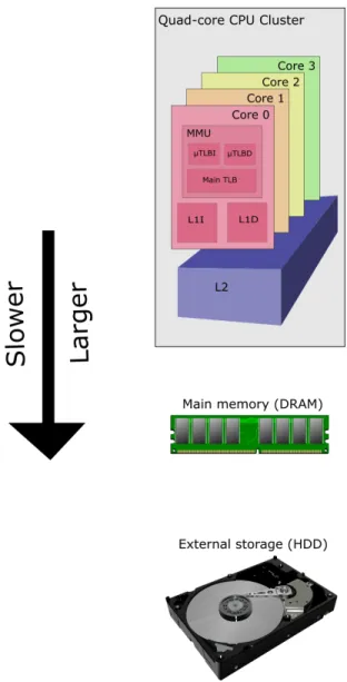
The entire memory hierarchy for an example computer with a quad-core processor, dynamic random access memory (DRAM) for main memory, and a hard disk drive (HDD) for secondary storage, is illustrated in Figure 1. Note that as you move down the diagram, each memory block gets larger in capacity and slower in access speeds.
2.2
Cache Design
The fundamental unit of a cache is the cache line, which is a specified minimum amount of con-tiguous information that can be inserted into or removed from a cache at a time. A cache line is several times larger than the minimum amount of information a CPU can process at a time, and is designed as such to take advantage of spatial locality. Thus, a cache can be viewed simply as an array of cache lines. Each cache line has an address that describes where in main memory it belongs.
Given that a cache has significantly less storage than main memory, there must be an efficient way to determine where in the cache a particular cache line should be placed. There are three fundamentally similar approaches, namely: direct mapped, set-associative, and fully-associative. The simplest design, the direct mapped approach, organizes a cache such that any given cache line can only be placed in a single specific location in the cache, directly determined by bits defined in the physical address. Alternatively, the cache can be designed such that a given cache line can be placed in a select few locations; the specific placement is at the discretion of the cache controller within the CPU. In this case, the cache would be described as N-way set-associative, where N is the number of possible locations for a given line, called ways. Each set of N ways is aptly referred to as aset, and the specific set a cache line is to be placed in is determined by bits defined in the physical address. Lastly, a cache is fully-associative if a given cache line can be placed anywhere within the cache. In the former two cases, the address bits that determine where in the cache a
line may be placed, i.e., what set it maps to, is referred to as itsindex.
Figure 1: Diagram of entire computer memory hierarchy. The smallest and fastest storage areas are the caches within each core, closely followed by the L2 cache outside the cores but within the CPU. External to the SoC is main memory, often in the form of DRAM, and the largest and slowest storage device: hard disk or solid state drives.
In addition to an index, each cache line has a correspondingtag, which is also specified by bits of the physical address. The tag is used to see if the address at a particular index matches the address that the CPU is looking for during lookups. This is necessary because multiple dif-ferent cache lines will map to the same index. In the case of a fully associative cache, there is no index, so the CPU will check the tag of every line in the cache to see if it matches the desired address. The offset indicates which subset of bytes of the cache line the CPU is requesting.
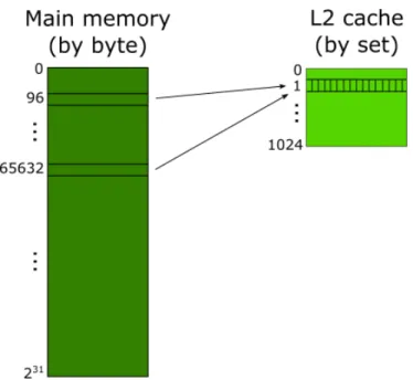
Figures 2 and 3 illustrate these properties for the Cortex-A15 in the Exynos 5250, which has 2GB of DRAM and a 1MB 16-way L2 cache with 64B cache lines [exy, A15]. Memory ad-dresses 96 and 65632 both map to set 1, but have differentiating tags. Since it is a 16-way set-associative cache, 14 more addresses can map to set 1 before lines must be evicted. Note that the decomposition in Figure 3 is computed from the hardware specifications given earlier. We know the offset is 6 bits long, since that is enough to fully address the 64B cache line. Similarly, we know the set number is 10 bits long, since there are 210sets:
1 MB cache size 64 B line size lines
16 lines/set = 2
10 sets
The tag then uses the remaining bits. Depending on the processor, some caches may be partitioned intobanks. Separate banks within the same cache can be accessed simulta-neously by different cores, which increases per-formance, and there can exist multiple levels of banking. For example, the ARM Cortex A15 has an L2 cache with four tag banks, selected by bits 6 and 7 of the physical address, and four data banks within each tag bank, selected by bits 4 and 5 of the physical address. In the example we give in Figures 2 and 3, the tag bank for each address is 1, and the data bank is 2. In
Figure 2: Two memory addresses map to the same 16-way L2 set in the Exynos 5250 Cortex-A15. Up to 16 set-congruent addresses can be stored per set in this cache at one time.
Figure 3: Address decomposition into tag, index, and offset for use in the cache. This information can be derived from the corresponding technical reference manuals.
this case, since the addresses map to the same banks, there is no performance benefit.
2.2.1 Cache Replacement Policies
When the CPU stores a new line into a cache that is full, it must first choose which cache line to evict to make room. This choice is governed by the cache’s replacement policy. The ideal replacement policy would choose the cache line that will not be needed for the longest time, but since this is usually impossible to know, algorithms such as least recently used (LRU), round robin (RR), and pseudorandom are used as approximations. See Table 1 for a listing of replacement policies in ARM Cortex processors.
2.2.2 Cache Coherency
Multi-core CPUs introduce the problem of cache coherency, in which the CPU must handle the possibility of caches in different cores holding different values for the same address. This will
Table 1: Cache replacement policies for specific processors [A7T, A15, A53b, A57, A72].
Processor L1I L1D L2
ARM Cortex-A7 Pseudorandom Pseudorandom Pseudorandom ARM Cortex-A15 LRU LRU Random ARM Cortex-A53 Pseudorandom Pseudorandom Undocumented ARM Cortex-A57 LRU LRU Random ARM Cortex-A72 LRU LRU Pseudo-LRU or Pseudorandom1 happen, for example, if one core modifies some data that is already present in another core’s cache. In this case, the respective L1 caches will not agree on the current value for the particular address. The solution is to either invalidate all copies of the data in all other caches, which lets the other cores know it is out-of-date, or to just update all copies of the data in the other caches. Two common approaches to implement cache coherency are to either have each core snoop
all requests and react appropriately, or use a logically-central directory that records shared data between cores. The snooping scheme elegantly takes advantage of the existing hardware bus connecting the cores by broadcasting all data requests. The directory scheme, on the other hand, allows for unicast messages between cores, which ultimately scales better.
2.2.3 Cache Maintenance
It is common for an instruction set architecture (ISA) to provide dedicated instructions that interact with the computer’s caches. These are used, for example, when the cache controller is ensuring coherency between cores, or in self-modifying code to ensure correct execution. One such instruction may mark a targeted cache line asinvalid, which is also known asinvalidating it. This is often as simple as flipping a single bit, which indicates it is outdated so that any future cache “hits” to this address instead go to memory as a cache miss. This has the same effect asflushing
the cache line, which removes its presence completely. There can also be instructions that clean
cache lines, which write adirtyline’s data out to memory if it has changed since being fetched into the cache. These cache maintenance operations may be combined or kept as distinct instructions, depending on the architecture. They may apply to only a specified cache, or to the entire cache hierarchy. Further, these instructions may require special permissions to be executed, depending on the processor.
Intel’s x86 ISA offers theclflush instruction [int], which cleans and then flushes all cache lines associated with a specified address from the entire cache hierarchy. This instruction is available from userspace. It also offersclflushopt as of the 6thgeneration of Intel Core processors, which is
identical in effect to clflush, but has better performance.
ARM offers dedicated instructions to clean a cache line based on a specific way, set, and cache level (L1 or L2), or by virtual address. In the latter case, the programmer must also indicate if coherency should be guaranteed from the perspective of input/output devices (such as a solid state drive), or if it must be guaranteed coherent only at the L2 cache. These are known as the
Point of Coherency and Point of Unification, respectively. Up until the recent ARMv8, these instructions were only available in privileged mode. In ARMv8, it is possible to allow a subset
of these maintenance instructions to be executed from userspace by setting the SCTRL EL1.UCI
bit2. Specifically, the userspace instructions are limited to [ARMb]:
DC CVAU Clean by virtual address to point of unification
DC CVAC Clean by virtual address to point of coherency
DC CIVAC Clean and invalidate by virtual address to point of coherency
IC IVAU Invalidate by virtual address to point of unification
The first three instructions affect data and the last instruction affects instructions, which can be surmised from the “DC” (data cache) and “IC” (instruction cache) initialisms.
It should be noted that operating systems may provide their own syscalls to allow execution of cache maintenance operations from userspace. For example, Linux and Android provide the
cacheflush syscall which cleans the given addresses in the L1D and invalidates them in the L1I. We believe this functionality was introduced for use in self-modifying code (which requires cleaned data and invalidated instructions to execute correctly). Until the ARMv8 Cortex-A53 processor, this syscall did not additionally invalidate the L2.
Thus, until ARMv8, there was no usable flush instruction in realistic, userspace attacks.
2.2.4 Cache Inclusiveness
In a system with multiple levels of caches, there is a design choice whether to allow lower level caches to hold data already present in higher level caches. Lower level caches areinclusive if they guarantee this property for all information in higher level caches, i.e., the higher level caches are a formal subset of the lower level caches. Caches areexclusive if they strictly forbid this property, such that a single address can only exist in one level of cache at a time. If the cache design does not implement one of these extremes, it is referred to as non-inclusive; information may or may not exist in multiple levels of cache at the same time. Although inclusiveness creates redundancy, thereby decreasing the total effective size of the processor’s cache, this effect is small since lower level caches are generally orders of magnitude larger than higher levels. Further, it simplifies cache coherency since it reduces the need for higher level caches to communicate with each other; they are guaranteed to be coherent since the inclusion property of the lowest level cache ensures they contain the same information.
If higher level caches are not unified, then the lower level cache’s inclusiveness may be specific to either the instruction or data cache. In this case, we refer to the lower level cache as either instruction-inclusive or data-inclusive. For brevity, we may refer to the higher level cache which is “included” in the lower level cache as the inclusive L1 cache, and we may refer to the lower level cache as either data or instruction inclusive.
2.2.5 Programmable Cache Lockdown
Some ARM processors support the ability to lock down parts of the cache such that data in specified set-ways will not be evicted, sometimes with the exception from cache maintenance operations, until the lockdown is removed. This feature largely depends on the system-on-chip (SoC), as the processors that do support it usually leave it implementation defined. The programmer can activate this feature by writing the appropriate system register with the desired way(s) to lock down, or indicating that subsequent line(s) allocated to the cache ought to be locked down. This type of lockdown is used primarily by real-time operating systems where guaranteed performance of small sections of code is required, such as interrupt handlers.
This programmable cache lockdown is orthogonal to the topic of this paper: the undocumented, implicit lockdown that prevents cores from evicting another core’s cache line. One obvious differ-ence is that a cache line that has been programmatically locked down cannot be evicted from any core, but a cache line that has been implicitly locked down can be evicted by the same core that locked it by filling the respective L1 cache. This is discussed in much more detail in Section 5.
The ARM Cortex A7, A15, and A57 explicitly document that they do not support the pro-grammable lockdown, however they all feature the implicit lockdown described in this paper.
3
Debugging ARM Processors
Debugging is a necessary and often time-consuming part of development. Present since ARMv4, basic external debugging has been upgraded into a wide variety of features that allow in depth control and information tracing. ARMv6 and ARMv7-A introduced rich application software platforms, like self-hosted debugging, which allows hardware and software to debug itself without the need for an external device, and performance profiling. ARMv7 defines basic debug facilities, such as breakpoints, watchpoints, and instruction execution in debug mode, at the architectural level. Finally, ARMv8 increased the level of control the debugger has over core-specific activity, and adds the ability to non-invasively collect large amounts of program execution data [ARMa].
ARM hardware can feature two different types of debugging capabilities: invasive and non-invasive. The former involves active interaction with program execution, while the latter is used to passively collect information.
Invasive debugging involves either an external device that connects to CPU cores via JTAG pins or a similar interface, or specific software on the same device that can monitor for debug events. It gives fine-grain control over program execution, for example, stopping program execution, or stepping through execution line by line, in terms of both C source lines and assembly instructions. Further, it allows for the inspection and modification of ARM registers and memory. Hardware breakpoints, which use comparators that trigger on specific addresses, are limited in number but can be used anywhere in memory without the need to modify code. Software breakpoints, on the other hand, can be used in large quantities, but only in DRAM, as they temporarily replace the target instruction with a BRK or HLT instruction. Additional debugging tools give support to more complicated breakpoints, like stopping on any instruction in a range of addresses, or only after a specific sequence of events or hardware state.
Invasive debugging is referred to as halting debug when using an external device, monitor debug if self-hosted, or semihosted, if it is a mix of both. In halting debug, debug events cause the particular core to enter a debug state, in which it stops fetching instructions from memory and instead executes under the direction of a debugger hosted elsewhere. The external debugger operates concurrently and possibly independently of the processor being debugged. In monitor debug, debug events cause a debug exception to be raised, which the monitor software must handle. Semihosting debug enables code on the target to use facilities of the debug host, for example, the keyboard input, screen output, and disk I/O. Like self-hosted debug, it is implemented through software instructions that generate exceptions. These are handled by the debug agent, which communicates with the host machine.
Non-invasive debugging does not actively interact with execution, but instead only observes the behavior of the core during execution. The main type of non-invasive debugging in ARM processors is known as trace. It can record memory accesses (both address and data), peripheral accesses, stack and heap accesses, and changes to variables. This data can be used to profile execution to find performance bottlenecks and provide call graph exploration, among other possibilities. Trace is provided by the embedded trace macrocell (ETM), as an internal hardware block connected to the core.
ARM-based SoCs. It expands the capabilities of the ETM to give more control to the debugger. For example, with CoreSight, one can control multiple cores synchronously, so when one hits a break-point, they all stop. CoreSight components include, but aren’t limited to:
Debug Access Port (DAP): Enables the external debugger to access system memory without putting the core into a debug state.
Embedded Cross Trigger (ECT): Links the debug capabilities of multiple devices, e.g., cores.
3.1
Performance Monitoring Unit
In additional to non-invasive debugging, there is available a performance monitoring unit (PMU) in modern ARM processors that can be used to gather statistics on processor operations and the memory system and analyze their performance. The PMU offers a small number of hardware counters (e.g., four in the Cortex-A7 and six in the A53) that can be programmed via registers to track the number of occurrences of certain events. Example events are the number of clock cycles that have elapsed, the number of DRAM accesses, the number of L1 misses, whether an exception has been taken, et cetera. A comprehensive list of events can be found in the technical reference manual for the given processor. The PMU registers are generally only accessible with elevated permissions, but there are system control registers that allow userspace access.
3.2
DS-5 and DSTREAM
ARM provides DS-5 Development Studio, an Eclipse-based feature-rich suite of development tools for ARM processors. The ultimate edition includes the LLVM-based ARM Compiler 6 and ARMv8 Fixed Virtual Platforms that give the ability to compile and debug code without needing target hardware. The debugging abilities of DS-5 ultimate edition include loading application images and debug symbols, running images, fundamental debugging features such as step-by-step execution and breakpoints, as well as application rewind, which lets the user debug the execution backwards. DS-5 ultimate edition can be used to debug bare-metal applications and Linux kernel and kernel modules using JTAG, and also to debug Linux applications using gdbserver. It features debug capabilities for bare-metal SMP systems, including cross-triggering and core-dependent views and breakpoints. Through ARM CoreSight, DS-5 also supports non-inclusive program trace. Among the many debugging tools provided by DS-5 is the Cache View window, which lets the user look into the L1, L2, and TLB caches of the processor cores. ARM also produces DSTREAM3, a debug
probe intended to accelerate development and device bring-up. It includes JTAG, CoreSight, TI, and MIPI adapters. Many features of DS-5 are only available if a DSTREAM unit is connected to the target hardware, as that is how it can exert control over the target.
A screenshot of DS-5 (and DSTREAM, though not shown) being used to debug a dual-core Cortex-A57 CPU is given in Figure 4. As pictured, DS-5 is partitioned into five windows, with two on the left and three on the right4. These will now be described in turn, moving left-to-right,
3https://www.arm.com/products/tools/arm-dstream-high-performance-debug-trace.php
4Note that there is much more to DS-5 than pictured in the screenshot. It has dozens of more windows that each provide functionality.
top-to-bottom:
• The top left window, “Debug Control”, allows the user to connect to the target hardware (physical or virtual), and control program execution on a per-cluster or per-core basis. The screenshot shows DS-5 is currently connected to two Cortex-A57 cores, and that program execution in both cores is currently stopped because a software breakpoint was triggered in core 0.
• The top right window is currently focused on “Cache View”, which gives the user visual access into the caches. The screenshot indicates that the L2 tags of core 0 are currently in view, and lists the metadata for several cache lines in sets 2 and 3. Note that the three cache ways visible in set 2 are all invalid, and are thus logically not in the cache, so their addresses are not displayed.
• The bottom left window is for editing source code. It can be seen that the debugger is currently stopped on a breakpoint on line 249 in file primes.c
• In the bottom right corner, there is the “Disassembly” window, which upon user request will show disassembled source code. However, it is not currently being used in the screenshot. Below that is the “App Console” window, which is used for I/O for the application being debugged.
3.3
Debugging on bare-metal
Instead of running an operating system, applications can be run on bare-metal, which gives the programmer full control over the embedded device’s hardware. This can be accomplished by programming the bootloader to load the programmer’s application image instead of the default OS image. The application must initialize the device’s components that would normally be handled in the OS, such as the MMU, the CPU caches, and secondary cores. A large benefit of running bare-metal is the elimination of background activity from the OS during computation. This is especially useful when debugging caches, as normal OS scheduling will inexorably pollute cache sets.
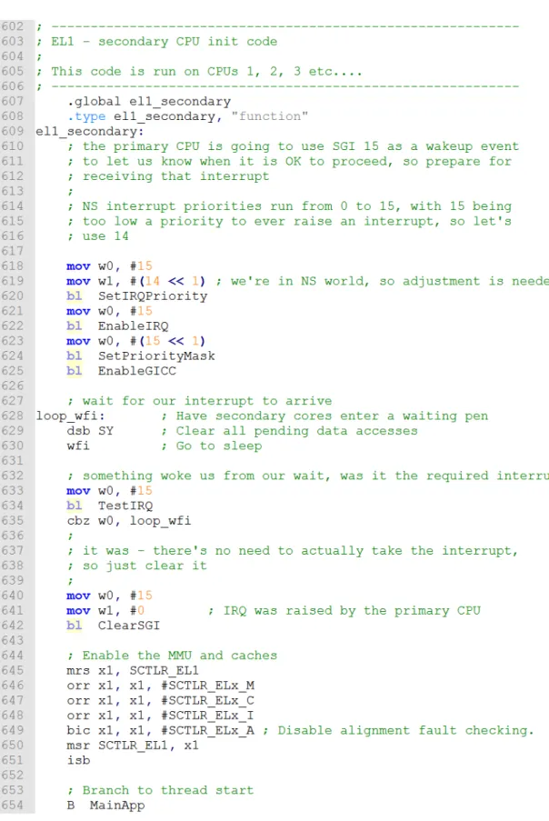
With DS-5 and DSTREAM, running metal is a matter of creating a corresponding bare-metal debug configuration and loading the desired bare-bare-metal application. This is accomplished by selecting the appropriate SoC, debug scenario, and application, via the debug configuration editor in DS-5. There is no significant difference in setup or methodology between debugging Linux (kernel, kernel module, or applications) and debugging bare-metal, besides the additional source code needed to initialize the hardware. Example code that handles device startup, hard-ware initialization, and running a user application is provided with DS-5 for single and multicore environments. A snippet of this code is given in Figure 5 for illustration. This code is responsible for powering on secondary cores; at this point in execution, the primary core has already started hardware initialization. Since most hardware initialization should only be done once, with the exception of core-specific resources like MMU configuration, secondary cores are put into a waiting
Figure 4: Screenshot of DS-5 Ultimate Edition debugging a Dual-core Cortex-A57 CPU with DSTREAM. The activ e connection can b e seen in th e top left corner; the execution breakp oin t can b e seen in source co de in the b ottom left corner; some of the tags found in the L2 cac he at this p oin t of execution can b e seen in the top righ t corner.
pen. This is done on lines 628 to 635, where the cores will spend most of their time sleeping on line 630. Once the primary core has finished initialization, it will send a software generated interrupt (SGI) to the secondary cores which will signal them to leave the waiting pen (line 635), initialize their own MMUs (lines 645 to 651), and branch to the main application code (line 654).
Figure 5: Code snippet provided by ARM to initialize secondary cores in a bare-metal debug setup. The primary core will initialize the non-core-private hardware resources while the secondary cores sleep.
4
Cache-timing Attacks
In cybersecurity, a side-channel attack is one that leverages weaknesses in the physical manifesta-tion of a system, rather than exploiting its theoretical basis. These side-channels can take the form of, but aren’t limited to, thermal energy, acoustic information, and EM radiation emission from a CPU, or hardware-related timing differences, during the execution of specific algorithms. The most well known type of channel attacks in this last category are known as cache-timing side-channels attacks, or cache attacks for short. These can glean sensitive information by measuring the execution time of selected instructions to determine if particular data is in the CPU’s cache. A common example involves discerning if instructions that depend on bits of a cryptographic secret key are executed, which indirectly reveals those bits of the key [YF14, ˙IGI+16].
4.1
History
Although cache attacks gained most of their popularity within the last five years, they are not a new phenomenon. In fact, as early as 1992, Hu already theoretically studied the effect of microarchitectural side channel attacks [Hu]. His work was later expanded by Page [Pag02] to introduce cache hits and misses as a covert channel to steal unauthorized information. This leakage was first observed by Tsunoo et al. [TSSS03], who utilized it to attack the DES block cipher. It was in 2004 when the first practical attacks against AES were introduced by both Bernstein [Ber04] and Osvik et al. [OST06]. While the first one based his analysis in collisions occurring during an AES encryption, the latter implemented two spy process techniques named Evict+Time and
Prime+Probe.
In the following years, several variants of the applicability of the aforementioned techniques were presented. For instance, in 2007, Aciimez utilized the Prime+Probe technique to steal an RSA secret key from the instruction cache [Acı] while Neve and Seifert utilized it to perform a last round AES attack [NS07]. Shortly after, Ristenpart et al. [RTSS] used the same technique to recover keystrokes from co-resident VMs, a work that would later be expanded by Zhang et al. [ZJRRb], proving the effectiveness of Prime+Probe to recover El Gamal cryptographic keys across VMs. Zhang et al. [ZJOR] further implemented aPrime+Probebased co-residency checker in IaaS clouds.
Although dangerous, all of the techniques described above were only shown to be successful in exploiting core private resources. Indeed, cache attacks did not start to show their entire potential until 2013, when Yarom and Falkner [YF14] (utilizing a similar technique as in [GBK], who recovered AES keys from a core co-resident user) presented the Flush+Reloadattack. This work, for the first time, demonstrated the viability of recovering RSA keys across cores and across VMs. Later, this analysis was expanded by Irazoqui et al. demonstrating the ability to recover AES keys and TLS session messages [IIES14, IIES15]. Further, Benger et al. [BvdPSY14] showed the feasibility of recovering ECC secret keys, Zhang et al. [ZJRRa] attacked e-commerce applications across PaaS VMs and Gruss et al. [GSM15] implemented template attacks with theFlush+Reload
technique.
require-ment. This requirement was bypassed by Liu et al. [Fan] and Irazoqui et al. [IES] by showing the feasibility of the Prime+Probe technique in the LLC, shared across cores. Later, Oren et al. [OKSK15] demonstrated that cache attacks are also applicable as javascript extensions, and Inci et al. [˙IGI+16] demonstrated the applicability of the technique in commercial IaaS clouds.
Re-cently, Lipp et al. [LGS+16] showed that both theFlush+Reloadtechnique and thePrime+Probe
technique, as well as the related Evict+Reload and Flush+Flush techniques, are applicable in mobile devices, including smartphone applications.
Recently, similar techniques have been shown to target very different aspects of the cache hier-archy to recover information. For instance, Irazoqui et al. [IES16] demonstrated the applicability of cache attacks across CPUs, Yarom et al. [YGH16] showed that cache bank contentions can also leak information, and Zhang et al. [ZXZ16] proved that theFlush+Reloadtechnique can be used instruction-side to mount ROP attacks in mobile devices. Further, Pessl et al. [PGM+16] utilized
cache priming techniques to implement DRAM access, and Gruss et al. utilized these techniques to implement cache prefetching attacks [GMF+16].
It is clear from these related works that there is an overwhelming majority of research dedicated to attacking Intel’s x86 architecture. Two of the few exceptions are the recent ARMageddon and ROP-based Flush+Reload papers [LGS+16,ZXZ16], which make several contributions to overcome the challenges of applying known x86 cache attacks on ARM. We discuss their methodology with respect to implicit cache lockdown in Section 5.
4.2
Practical Considerations
This section discusses practical techniques common among cache-timing attacks. These can differ between microarchitectures, but our discussions will primarily focus on ARM.
4.2.1 Cache Line Eviction
Some of these attacks require evicting information from the cache. This can be done by leveraging the limited set-associativity of the underlying hardware. For example, to evict a cache line from a 4-way set-associative L1D, the attacker must force the L1D to fetch at least 4 distinct set-congruent lines, which would optimally fill all 4 ways of that particular set, forcing the target cache line to be evicted. However, the replacement policy of the cache affects the ability to do this. In LRU policies, this optimal situation will occur, since by the fourth consecutive fetch, the target cache line is guaranteed to be the least recently used cache line. In pseudorandom replacement policies, there is no guarantee that the target cache line will ever be selected to be evicted. Despite this, researchers have shown that an optimal eviction strategy can be found for any processor through trial and error [GSM15, LGS+16]. Intel processors generally use a LRU replacement policy in
their caches, but ARM processors can have differing replacement policies between processors and even between cache levels within the same processor, as previously shown in Table 1. While surmountable, this increases the complexity of attacking ARM devices.
An example eviction strategy for the Cortex-A53 is given in Algorithm 1 to show the structure of the “sliding window” techniques from [LGS+16]. The number of iterations within eachforloop
varying the number of these iterations, one can find the minimum number of memory accesses needed for guaranteed eviction for a given processor.
Algorithm 1:An example eviction strategy for the Cortex-A53.
Input: addrs, a list of set-congruent addresses
1 fori= 0..24do /* start of sliding window */
2 forj= 0..1 do /* number of repetitions per window */
3 fork= 0..5do /* number of addresses per window */
4 accessaddrs[i+k];
5 end
6 end 7 end
Since caches operate on physical addresses, finding set-congruent addresses when running bare-metal is a simple matter of algebra, since there aren’t obfuscating virtual addresses. On Linux, physical addresses can be found by consulting /proc/[pid]/pagemap for a particular pro-cess, which lists mappings between virtual and physical addresses. For any given physical address, set-congruent addresses can be found with knowledge of the cache structure. Specifically, incre-menting thetagof a physical address will result in the first sequential address that is set-congruent. This is because doing so keeps all lower bits, namely those that comprise theset number, the same, and therefore the address will map to the same set.
The manner in which a set-congruent address is accessed differs depending on whether it is data or an instruction. Data addresses can be accessed by loading their content to a register with theLDR assembly instruction. Instruction addresses can be accessed by executing abranch
instruction that jumps to it. Multiple set-congruent instructions can be accessed in a row, as per Algorithm 1, by first enumerating several thousand function calls to a dummy function, a small subset of which will be on set-congruent memory lines. This dummy function will keep track of the sliding window and branch to a subsequent set-congruent function call. In this manner, by ensuring the dummy function is not composed of set-congruent instruction addresses, cache pollution is prevented.
For reference in this and later sections, we use the termself-evictionto describe when a proces-sor’s core evicts a cache line from its own L1 cache, regardless of intention. This is to distinguish from an attacking core evicting a cache line from a victim core’s L1 cache. In either case, the group of set-congruent addresses used to evict the targeted cache line is referred to as an eviction set.
4.2.2 Timing Memory Accesses
One fundamental aspect of cache-timing attacks is the ability to accurately time memory accesses. The PMU has an event that corresponds to the number of elapsed clock cycles. Since clock speeds are generally consistent throughout execution, it can be used to compare relative execution times between sets of instructions. While the PMU is not directly accessible by userspace applications by default, there has been an unprivleged syscall available in Linux 2.6.31 that acts as a wrapper to the cycle counter. [LGS+16] thoroughly discusses this and two other methods of measuring
time that are available from userspace: a POSIX timing function and a dedicated thread counter. This latter option simply spawns a thread to solely increment a variable in an infinite loop. Since this read-increment-write sequence generally takes a consistent number of cycles to execute, this provides a high enough resolution to distinguish cache hits from misses.
4.2.3 Shared Memory
Shared memory refers to when multiple processes each have data in their own virtual address spaces, possibly with distinct virtual addresses from each other, that all map to the same physical addresses. This can be used to easily share data across processes, and can also be used to remove seemingly needless redundancy in main memory. However, by removing the memory isolation given to processes by virtual addressing, shared memory can be used by attackers to influence a victim process’ memory address space. Indeed, Flush+Reload leverages this principle.
Memory deduplication is one instance of shared memory. In this case, the kernel will period-ically scan physical memory for duplicate frames. Upon finding one, if the kernel determines the frames will not be updated frequently, it will merge them into one frame and update the corre-sponding virtual address spaces. The kernel will mark this shared memory as copy-on-write so that if one process modifies the data, it will be copied to another location as to not affect other processes. An example of deduplication mechanisms is Kernel Same-page Merging (KSM), imple-mented in every Linux operating system (and consequently in the KVM hypervisor) by default. Another example is VMware’s Transparent Page Sharing (TPS), which was a default feature until 2014. A second instance of shared memory is brought about through the usage of shared libraries, which refer to precompiled code that can be used by multiple applications. Shared libraries are extensively used in all major operating systems.
4.3
Known Cache Attacks
In this section, we describe known cache-timing attacks and the differences in their implementations between Intel and ARM processors. We also mention the farthest architectural-distance achieved when performing each of these attacks; the more architecturally distant the attacker and victim are, the more realistic and severe the attack.
The overarching goal of these attacks is to determine the data that a given victim process operate on. This data is often intended to be sensitive, such as cryptographic keys. This can be done, for example, by trying to glean that specific data directly, or by analyzing the code the victim process will execute, and inferring the data based on discerning the exact execution path. The following cache attacks work in the general case; it is up to the attacker to apply them on a case-by-case basis.
4.3.1 Evict+Time
Evict+Time, summarized in Algorithm 2, uses timing measurements to determine which cache sets are occupied by the victim’s algorithm, whatever it may be. The idea is to time the algorithm’s execution before and after selectively evicting hypothesized addresses from the cache. By
compar-ing the execution times, the attacker gains insight into whether the selected addresses are used by the algorithm. Specifically, if the addresses were indeed used, the executions will take a similar amount of time. Otherwise, the second execution is likely to be faster because it has more data in the cache. Note that the attacker needs to run the eviction algorithm once before measuring its execution time so that the latter two executions both run with a similar amount of cached data (excluding the data being tested). The very first execution of the algorithm will always take a longer amount of time because it does not have any cached data; all of its memory accesses will come from DRAM (assuming an initial clean cache). The second and third executions, the ones being timed, will be able to use some data that is already in the cache.
However, it is possible that the results of Evict+Time can be misleading. For example, if the algorithm self-evicts its own data during execution, then both executions may take a similar amount of time regardless of the attacker’s eviction. Furthermore, the algorithm may not have consistent execution time to begin with, possibly due to its size, its nature, or the method by which it is invoked (e.g., by a noisy kernel system call).
Evict+Time has only been shown to work in Intel processors [OST06], but we are confident it would work just as well in ARM processors. It has also yet to be applied in the LLC for cross-core attacks. If an attacker desires to apply Evict+Time across cross-cores, she can only apply it in an inclusive LLC since she needs to evict the victim’s upper level caches. We believe the lack of attention given to Evict+Time is due to the better practicality of the Prime+Probe attack.
Algorithm 2:Evict+Time
1 Run victim’s algorithm once to load its data and instructions into the cache. 2 Run victim’s algorithm a second time, measuring its execution time.
3 Evict from the cache address(es) possibly used by the algorithm.
4 Run victim’s algorithm a third time, measuring its execution time again.
5 if Execution times similar thenConclude targeted address(es) likely used by algorithm; 4.3.2 Prime+Probe
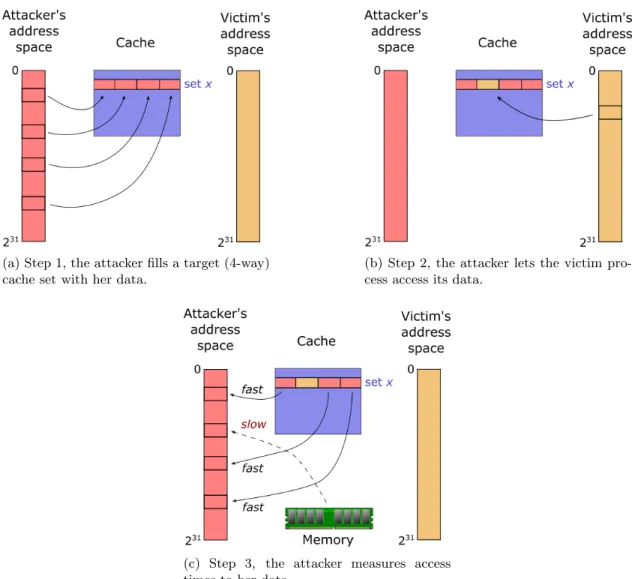
Prime+Probe, like Evict+Time, is an attack that can identify cache sets used by the victim’s algorithm. As described in Algorithm 3, it does so by determining which cache-primed memory lines have slow access times after running the victim’s algorithm. Slow access times indicate that the address is being fetched from DRAM, which implies it must have been evicted from cache. The idea is to execute steps 1-3 with as little delay as possible, so that the only reason cache evictions could occur would be from the victim’s algorithm. This is illustrated in Figure 6.
Algorithm 3:Prime+Probe
1 Prime cache set by accessing set-congruent addresses 2 Execute victim’s algorithm.
3 Time how long it takes to re-access (probe) each address.
4 if Access times are slow thenConclude targeted set is used by algorithm;
As with Evict+Time, Prime+Probe only works under the assumption of inclusive caches. Oth-erwise, the attacker would not be able to evict the set occupied by the targeted memory block
(a) Step 1, the attacker fills a target (4-way) cache set with her data.
(b) Step 2, the attacker lets the victim pro-cess acpro-cess its data.
(c) Step 3, the attacker measures access times to her data.
Figure 6: High-level overview of the Prime+Probe attack corresponding to Algorithm 3. If the access times in step 3 are relatively slow, that indicates they were evicted from the cache by the victim process.
in the victim’s L1 cache in Step 1. However, unlike Evict+Time, Prime+Probe does not time the execution of the algorithm under attack. Instead, it times the relatively noise-free execution of its own memory accesses, providing an access pattern over time, thereby increasing resolution, reliability, and providing wider applicability.
Prime+Probe has been shown to work cross-core in Intel [IES] and ARM [LGS+16]. The
only implementation differences are related to processor-dependent parameters, such as the cache associativity.
4.3.3 Flush+Reload
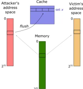
The Flush+Reload attack, outlined in Algorithm 4 and illustrated in Figure 7, also provides information on the memory addresses used by the victim, and consequently the data on which it
operates. However Flush+Reload implements a slightly different approach than Evict+Time and Prime+Probe, as it operates on shared data between victim and attacker. Like Prime+Probe, the attacker only measures accesses made by her own attacking algorithm. By using shared memory and the architecture’sflushinstruction, Flush+Reload guarantees a quick removal of the targeted memory address. This improvement allows for a greater resolution and lower noise because there is a larger percentage of time that can be devoted to waiting for the victim.
Although the shared memory requirement might seem unrealistic, it can be easily satisfied by an attacker with shared libraries or memory deduplication. This is discussed in Section 4.2.3.
The Flush+Reload attack does not require the inclusiveness property to succeed. Due to shared memory, the flush stage invalidates the data throughout the entire cache hierarchy, including the victim’s private L1 caches. As the cache coherency protocol has to ensure coherency even across CPU sockets, the attack also works across CPUs in Intel and ARMv8, as pointed out in [IES16,LGS+16]. The reload stage will be fast if the targeted memory line is in the cache. Since
it was flushed from the cache just prior, it will only be in the cache if the victim has accessed it. In Intel, the cache flush instruction isclflush, and indeed, it invalidates the given address from the entire cache hierarchy. In ARM, the situation is slightly more complicated. Linux or Android, when running on ARMv7 (and potentially prior), offer an ARM specific syscall, cacheflush, to clean the L1D and invalidate the L1I of the specified address. Note that only the instruction side is invalidated; the data side is not. However, in ARMv7 processors, this operation does not affect the entire hierarchy. Namely, L2 cache lines are not invalidated even if they were invalidated in the L1I [ZXZ16]. Thus, lacking any userspace flush instruction, Flush+Reload is not realistically possible on ARMv7. This is not the case with ARMv8: the cacheflush syscall does flush the L2 on the ARM Cortex-A53 [ZXZ16], thereby permitting instruction-side Flush+Reload attacks. Further, it is possible to to enable userspace data invalidation hardware instructions in ARMv8, as described in 2.2.3. When enabled, this allows data-side Flush+Reload attacks to be conducted, as demonstrated in [LGS+16].
Algorithm 4:Flush+Reload
1 Flush specific memory line(s) from entire cache hierarchy. 2 Allow victim time to access memory line(s).
3 Time the reload of the memory line(s).
(a) The initial state before the Flush+Reload attack. The attacker shares a memory ad-dress with the victim, which may already be in the cache.
(b) Step 1, the attacker flushes the memory line from the cache.
(c) Step 2, the attacker lets the victim exe-cute, possibly accessing the shared memory.
(d) Step 3, the attacker reloads the memory. If the reload comes from the cache (pictured), it will be relatively quick.
Figure 7: High-level overview of the Flush+Reload attack corresponding to Algorithm 4. If the reload step is relatively slow, the target cache line must have been loaded from main memory, indicating the victim process did not access it.
4.3.4 Evict+Reload
Evict+Reload, described in Algorithm 5, combines characteristics of the Prime+Probe and Flush+Reload attacks. Instead of using the full-hierarchical flush instruction, removal of the targeted memory from the cache hierarchy is performed with an eviction set, like in Prime+Probe. This is useful when there is no userspace flush instruction, such as in ARMv7 and earlier, and in ARMv8 when flush is unavailable from userspace. For eviction to affect the relevant elements of the cache hierarchy, the processor being attacked must be inclusive with respect to the type of information the attacker is utilizing, data or instruction, like in Prime+Probe. Evict+Reload has yet to be shown to work across CPUs. Since the flush instruction is what cross-CPU Flush+Reload relies on—flush invalidates shared data regardless of location in the cache hierarchy—we are not sure if Evict+Reload can be applied cross-CPU. This attack has been carried out on both Intel and ARM processors [GSM15, LGS+16], without significant difference between implementations
except processor-dependent parameters (e.g., cache associativity).
Algorithm 5:Evict+Reload
1 Evict specific memory line(s) from entire cache hierarchy. 2 Allow victim time to access memory line(s).
3 Time the reload of the memory line(s).
4 if Reload is fast thenConclude memory line is used by algorithm; 4.3.5 Flush+Flush
Flush+Flush leverages the observation that the architecture’s flush instruction can abort early if it detects a cache miss. Thus, timing measurements of the flush instruction can be used to determine if a targeted memory addresses is present in the cache or not. Unlike the other cache attacks, Flush+Flush does not access memory itself, but instead simply repeatedly times the execution of the flush instruction, as described in Algorithm 6.
This attack has been shown to work in both Intel and ARMv8 processors [GMWM16,LGS+16],
with the only difference between them being the architecture-dependent flush instruction.
As in the case of Flush+Reload, the Flush+Flush attack does not require cache inclusion to succeed, and works even when victim and attacker reside in different CPUs.
Algorithm 6:Flush+Flush
1 whileTrue do
2 Time the flush of specific memory line(s) from entire cache hierarchy. 3 if Flush is fast thenConclude memory line has not been used by algorithm; 4 end
5
Implicit Cache Lockdown
We have observed behavior in several ARM Cortex-A processors that restricts the ability of one CPU core to evict information residing in another core’s L1 cache. We call this behavior im-plicit cache lockdown, to differentiate it from the programmable cache lockdown discussed in Sec-tion 2.2.5.
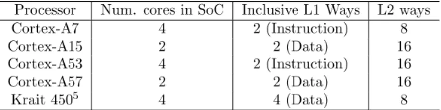
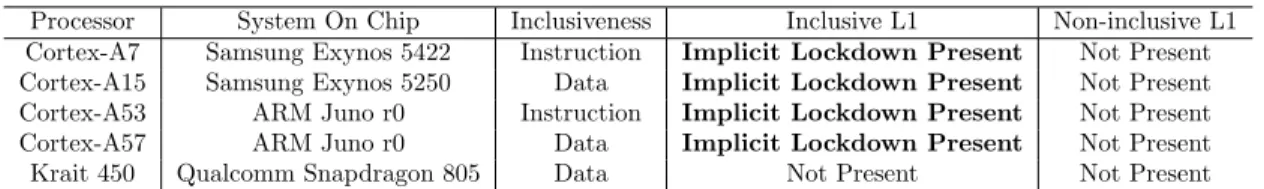
Specifically, we observe that a cache line in a core’s inclusive L1 cache, and thus also in the L2 cache, will remain in these caches until evicted by the same core that allocated it. This effectively “locks down” the particular way of the corresponding cache set from the perspective of other cores, as they are not able to evict it or allocate new data to it. We have observed this behavior holds true for as many ways as the inclusive L1 cache has per core, and can happen simultaneously in multiple cores. This eviction restriction even extends to the other L1 cache (recall there is a data L1 cache and an instruction L1 cache per core) in the same core that is locking down ways: the core’s non-inclusive memory cannot evict information from the inclusive L1 cache. Thus, a large portion of the L2 cache may be effectively unusable by a particular core if the other cores in the CPU have allocated lines in their own inclusive L1 caches. Referring to Table 2, one can see that in the Quad-core Cortex-A7, there are four 2-way L1I caches, which means it is possible for the entire 8-way L2 cache to be locked down by the instruction caches. In this case, data would not be able to be allocated to the L2 until one of the cores self-evicts (i.e., evicts a line itself due to normal cache activity), or until a privileged cache maintenance operation invalidates a cache line. This effect is also present in the other processors, but to a lesser degree. In the A15 and A57, 4 ways, or 25% of the L2, can be locked down at once. In the A53, up to 8 ways, or 50% of the L2, can be locked down at once.
Table 2: Set-associativity of ARM and ARM-based processors Processor Num. cores in SoC Inclusive L1 Ways L2 ways Cortex-A7 4 2 (Instruction) 8 Cortex-A15 2 2 (Data) 16 Cortex-A53 4 2 (Instruction) 16 Cortex-A57 2 2 (Data) 16 Krait 4505 4 4 (Data) 8
Note that this behavior holds even in the absence of subsequent activity in the other cores; their initial allocation to their inclusive L1 is all that is needed to lock down the way in the L2, forever6.
Our experiments demonstrate this behavior only exists in the inclusive L1 caches of each pro-cessor. All of the tested processors have separate instruction and data L1 caches, and all but the A7 and A53 are data-inclusive.
We have only found the lockdown behavior to exist in ARM processors. In our experiments with the Qualcomm Snapdragon Krait architecture, which uses the ARM instruction set but has
5No official public documentation for this architecture exists, but the table lists what we found through experi-mentation and online articles [kra].
6I.e., until they evict the line themselves, or a relevant privileged cache maintenance instruction is executed, such asDC CIVAC.
![Table 1: Cache replacement policies for specific processors [A7T, A15, A53b, A57, A72].](https://thumb-us.123doks.com/thumbv2/123dok_us/10174373.2919734/14.918.163.755.139.247/table-cache-replacement-policies-specific-processors-a-t.webp)